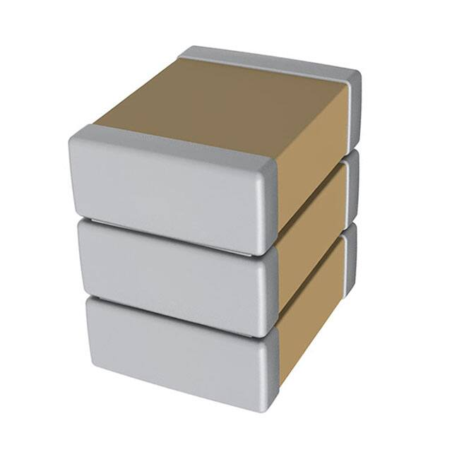
Surface Mount Multilayer Ceramic Chip Capacitors (SMD MLCCs)
U2J with KONNEKT™ Technology for High-Efficiency,
High-Density Power Applications (Commercial Grade)
Lead-free
Overview
KEMET's U2J with KONNEKT™ Technology surface
mount capacitors are designed for high-efficiency and
high-density power applications. KONNEKT utilizes
an innovative Transient Liquid Phase Sintering (TLPS)
material to create a leadless multi-chip solution. When
combined with KEMET’s ultra-stable U2J dielectric,
KONNEKT enables a low-loss, low-inductance package
capable of handling extremely high ripple currents in the
hundreds of kilohertz.
U2J is an extremely stable Class I dielectric material that
exhibits a negligible shift in capacitance with respect to
voltage and a predictable and linear change in capacitance
with reference to ambient temperature, with minimal
aging effect. Capacitance change is limited to –750 ±120
ppm/°C from –55°C to +125°C.
U2J with KONNEKT™ Technology can also be mounted
in a low-loss orientation to further increasing its power
handling capability. The low-loss orientation lowers ESR
(Effective Series Resistance) and ESL (Effective Series
Inductance) which increases ripple current handling
capability.
Benefits
Applications
• Extremely high-power density and ripple current
capability
• Extremely low equivalent series resistance (ESR)
• Extremely low equivalent series inductance (ESL)
• Operating temperature range of −55°C to +125°C
• Retains over 99% of nominal capacitance at
full rated voltage
• Low noise
• Surface mountable using standard MLCC reflow profiles
• Low-loss orientation option for higher current handling
capability
• RoHS compliant and Pb-free
• Wide bandgap (WBG), silicon carbide (SiC) and gallium
nitride (GaN) systems
• Data centers
• LLC resonant converters
• Switched tank converters
• Wireless charging systems
• Photovoltaic systems
• Power converters
• Inverters
• DC link
• Snubber
Standard
Low Loss
Built Into Tomorrow
© KEMET Electronics Corporation • KEMET Tower • One East Broward Boulevard
Fort Lauderdale, FL 33301 USA • 954-766-2800 • www.kemet.com
C1097_KONNEKT_U2J • 8/25/2021
1
�Surface Mount Multilayer Ceramic Chip Capacitors (SMD MLCCs)
U2J with KONNEKT™ Technology for High-Efficiency, High-Density Power Applications (Commercial Grade)
Typical Performance
Typical Ripple Current (A rms)1
Part Type
Mounting
Configuration
Typical ESR at
25°C, 100 kHz
Typical ESL
at 25°C
100 kHz
200 kHz
300 kHz
Standard
1.15 mΩ
1.1 nH
12.0
12.0
11.5
Low Loss
0.77 mΩ
0.45 nH
18.0
18.0
16.0
Standard
1.3 mΩ
1.6 nH
11.0
10.0
10.0
Low Loss
0.35 mΩ
0.4 nH
20.0
34.0
31.0
1812
940 nF
1812
1.4 uF
Ripple current measurements performed at 85°C with a peak capacitor temperature of 95°C. Samples mounted to heat sink with no forced air cooling.
Maximum ambient and self heating cannot exceed 125°C.
1
ESR (mOhms)
Impedance (Ohms)
1812 940 nF 50 V
1812 940 nF 50 V
1,000.00
Standard
100.00
Impedance (Ohms)
1,000.00
Low-Loss
Standard
Low-Loss
100.00
ESR (mOhms)
10.00
1.00
0.10
10.00
1.00
0.01
0.10
0.00
1
10
100
1,000
10,000
1
100,000
10
100
Impedance (Ohms)
Low-Loss
1.00
0.10
1
10
Capacitance change (%)
Capacitance change (%)
5
0
-5
-10
5
25
45
65
85
105
10
5
0
-5
-10
125
0
Temperature (°C)
Ripple Current 1812 940 nF 50 V (A )
Standard
rms
)
Low-Loss
)
10
20
30
40
50
DC Voltage (V)
© KEMET Electronics Corporation • KEMET Tower • One Eastrms
Broward Boulevard
50
30
Fort Lauderdale,
FL 33301 USA • 954-766-2800 • www.kemet.com
rms
1,000
Capacitance Change vs DC Voltage
KONNEKT U2J
10
-15
100
Frequency (kHz)
Capacitance Change vs Temperature
KONNEKT U2J (Typical)
-35
100,000
0.10
100,000
Frequency (kHz)
-55
10,000
1.00
0.00
10,000
Low-Loss
10.00
0.01
1,000
Standard
100.00
10.00
ESR (mOhms)
Impedance (Ohms)
1,000.00
Standard
100.00
100
100,000
1812 1.4 uF 50 V
1,000.00
10
10,000
ESR (mOhms)
1812 1.4 uF 50 V
1
1,000
Frequency (kHz)
Frequency (kHz)
40
Ripple Current 1812 1.4
uF 50 V (Arms)• 8/25/2021
C1097_KONNEKT_U2J
Standard
Low-Loss
2
�Capacitance chang
Capacitance change (
5
0
Surface Mount
Multilayer Ceramic Chip Capacitors (SMD MLCCs)
-5
5
0
-5
U2J with KONNEKT™ Technology for High-Efficiency, High-Density Power Applications (Commercial Grade)
-10
-55
-35
-15
5
25
45
Temperature (°C)
Typical Performance cont.
65
85
105
-10
125
0
20
30
40
50
DC Voltage (V)
Ripple Current 1812 1.4 uF 50 V (Arms)
Ripple Current 1812 940 nF 50 V (Arms)
30
50
Standard
Ripple Current (Arms)
Low-Loss
Ripple Current (Arms)
10
20
10
Standard
Low-Loss
40
30
20
10
0
0
0
50
100
150
200
250
300
0
350
50
100
150
200
250
300
350
Frequency (kHz)
Frequency (kHz)
Ordering Information
C
1812
C
145
Series
Case Size
(L"x W")
Specification/
Series
Capacitance
Code (pF)
1812
C=
Standard
Two single
digits and
number of
zeros.
C=
Ceramic
J
5
J
L
C
7XXX
Termination
Finish1
Packaging
(Suffix/C-Spec)
C = 100% matte Sn
See
"Packaging
C-Spec
Ordering
Options
Table"
Subclass
Capacitance
Rated
Dielectric
Designation
Tolerance Voltage (V)
J = ±5%
K = ±10%
5=
50 V
J=
U2J
L=
KONNEKT
Additional termination finish options may be available. Contact KEMET for details.
See Table 1A for available capacitance and voltage ratings.
1
Table 1A - Product Ordering Codes, Ratings, and Package Quantities
KEMET
Part Number1
C1812C944(a)5JLC(b)
C1812C145(a)5JLC(b)
Capacitance
940 nF
1.4 µF
Cap
Code
944
145
Voltage
50 V
50 V
Number
of Chips
Orientation
Thickness
mm (inch)
Standard
3.5 (0.137)
±0.40 (0.016)
Low Loss
3.20 (0.126)
±0.30 (0.012)
Standard
5.3 (0.208)
±0.60 (0.024)
Low Loss
3.20 (0.126)
±0.30 (0.012)
2
3
Typical
Average
Piece
Weight
(g)
0.22
0.33
Tape & Reel Quantity
7" Tape & Reel
13" Tape & Reel
500
2,000
500
2,200
200
900
500
2,200
Complete part number requires additional characters in the numbered positions provided in order to indicate capacitance tolerance and grade.
For each numbered position, available options are as follows:
(a) Capacitance tolerance character "J" or "K"
(b) See Table 1B for C-Spec options
1
© KEMET Electronics Corporation • KEMET Tower • One East Broward Boulevard
Fort Lauderdale, FL 33301 USA • 954-766-2800 • www.kemet.com
C1097_KONNEKT_U2J • 8/25/2021
3
�Surface Mount Multilayer Ceramic Chip Capacitors (SMD MLCCs)
U2J with KONNEKT™ Technology for High-Efficiency, High-Density Power Applications (Commercial Grade)
Table 1B - Packaging C-Spec Ordering Options Table
Mounting Orientation
Standard
Low Loss
Packaging Type
Packaging/Grade
Ordering Code (C-Spec)
7" Reel/Unmarked
TU
13" Reel/Unmarked
7210
7" Reel/Unmarked
7805
13" Reel/Unmarked
7810
Dimensions – Millimeters (Inches)
Standard Mounting
2 Chips
W
Low Loss Mounting
2 Chips
L
L
B
Standard Mounting
3 Chips
W
W
Low Loss Mounting
3 Chips
L
L
B
W
B
B
T
Number
of Chips
2
3
Mounting
EIA
SIZE
CODE
METRIC
SIZE
CODE
L
LENGTH
W
WIDTH
T
THICKNESS
B
BANDWIDTH
Mounting
Technique
4.50 (0.177)
±0.30 (0.012)
3.2 (0.126)
±0.3 (0.012)
3.5 (0.137)
±0.4 (0.016)
3.2 (0.126)
±0.3 (0.012)
5.3 (0.208)
±0.6 (0.024)
3.5 (0.137)
±0.4 (0.016)
3.2 (0.126)
±0.3 (0.012)
5.3 (0.208)
±0.6 (0.024)
3.2 (0.126)
±0.3 (0.012)
0.6 (0.024)
±0.35 (0.014)
Solder
Reflow
Only
Standard
Low Loss
Standard
Low Loss
1812
T
T
T
4532
© KEMET Electronics Corporation • KEMET Tower • One East Broward Boulevard
Fort Lauderdale, FL 33301 USA • 954-766-2800 • www.kemet.com
C1097_KONNEKT_U2J • 8/25/2021
4
�Surface Mount Multilayer Ceramic Chip Capacitors (SMD MLCCs)
U2J with KONNEKT™ Technology for High-Efficiency, High-Density Power Applications (Commercial Grade)
Table 2 - Performance and Reliability: Test Methods and Conditions
Test
Reference
Test Condition
Limits
Visual and
Mechanical
KEMET
Internal
No defects that may affect performance (10X)
Dimensions according KEMET Spec Sheet
Capacitance
(Cap)
KEMET
Internal
Dissipation
Factor (DF)
KEMET
Internal
Insulation
Resistance (IR)
KEMET
Internal
1 kHz ±50 Hz and 1.0 ±0.2 Vrms
Capacitance measurements (including tolerance) are
indexed to a referee time of 1,000 hours
1 kHz ±50 Hz and 1.0 ±0.2 Vrms
Apply rated voltage for 120 seconds at 25°C
Within Tolerance
Dissipation factor (DF) maximum limit at 25°C = 0.1%
Within Specification
To obtain IR limit, divide MΩ-µF value by the
capacitance and compare to GΩ limit. Select the
lower of the two limits.
1,000 MΩ-µF or 100 GΩ
Frequency: 1 kHz ±50 Hz
Capacitance Change with Reference to +25°C
and 0 VDC Applied
Temperature
Coefficient of
Capacitance
(TCC)
* See part number specification sheet for voltage
KEMET
Internal
Step
Temperature (°C)
1
+25°C
2
−55°C
3
+25°C (Reference Temperature)
4
+125°C
Dielectric
Withstanding
Voltage
(DWV)
KEMET
Internal
250% of rated voltage
(5 ±1 seconds and charge/discharge
not exceeding 50 mA)
Aging Rate
(Maximum %
Capacitance
Loss/Decade
Hour)
KEMET
Internal
Capacitance measurements (including tolerance) are
indexed to a referee time of 1,000 hours. Please refer to
a part number specific datasheet for referee time details.
−750 ±120 ppm/°C
Cap: Initial Limit
DF: Initial Limit
IR: Initial Limit
Withstand test voltage without insulation
breakdown or damage.
0.1% Loss/Decade Hour
Shear stress test per specific case size,
Time: 60±1 seconds
Terminal
Strength
KEMET
Internal
Case Size
Force
1812
18N
© KEMET Electronics Corporation • KEMET Tower • One East Broward Boulevard
Fort Lauderdale, FL 33301 USA • 954-766-2800 • www.kemet.com
No evidence of mechanical damage
C1097_KONNEKT_U2J • 8/25/2021
5
�Surface Mount Multilayer Ceramic Chip Capacitors (SMD MLCCs)
U2J with KONNEKT™ Technology for High-Efficiency, High-Density Power Applications (Commercial Grade)
Table 2 - Performance and Reliability: Test Methods and Conditions cont.
Test
Reference
Test Condition
Limits
Standard Termination system 2.0 mm
Test time: 60± 5 seconds
Ramp time: 1 mm/second
Board
Flex
AEC-Q200-005
Solderability
KEMET
Custom Test
Temperature
JESD22
Cycling
Method JA-104
Biased
Humidity
MIL-STD-202
Method 103
No evidence of mechanical damage
1. Board shear – SAC305 solder. Shear force of 1.8 kg
(minimum)
2. Wetting balance – IEC 60068–2–69
1,000 cycles (−55°C to +125°C)
2-3 cycles per hour
Soak Time 1 or 5 minute
Load Humidity:
1,000 hours 85°C / 85% RH and rated voltage,
or 200 VDC maximum.
Low Volt Humidity:
1,000 hours 85C°/85% RH and 1.5 V.
Visual Inspection. 95% coverage on termination. No
leaching.
Measurement at 24 hours
±4 hours after test conclusion.
Cap: Initial Limit
DF: Initial Limit
IR: Initial Limit
Measurement at 24 hours ±4 hours
after test conclusion.
Within Post Environmental Limits:
Cap: ±0.3% or ±0.25pF shift
IR: 10% of Initial Limit
DF Limits Maximum: 0.5%
Measurement at 24 hours ±4 hours
after test conclusion.
Moisture
Resistance
MIL-STD-202
Method 106
Number of cycles required 10, 24 hours per cycle.
Steps 7a and 7b not required
Thermal
Shock
MIL-STD-202
Method 107
Number of cycles required 5, (-55°C to 125°C)
Dwell time 15 minutes.
© KEMET Electronics Corporation • KEMET Tower • One East Broward Boulevard
Fort Lauderdale, FL 33301 USA • 954-766-2800 • www.kemet.com
Within Post Environmental Limits
Cap: ±0.3% or ±0.25pF shift
IR: 10% of Initial Limit
DF Limits Maximum: 0.5%
Cap: Initial Limit
DF: Initial Limit
IR: Initial Limit
C1097_KONNEKT_U2J • 8/25/2021
6
�Surface Mount Multilayer Ceramic Chip Capacitors (SMD MLCCs)
U2J with KONNEKT™ Technology for High-Efficiency, High-Density Power Applications (Commercial Grade)
Table 2 - Performance and Reliability: Test Methods and Conditions cont.
Test
High
Temperature
Life
Reference
Test Condition
1,000 hours at 125°C with 1.0 X rated voltage applied.
MIL-STD-202
Method 108
Storage Life
1,000 hours at 125°C, Unpowered
Limits
Within Post Environmental Limits
Cap: ±0.3% or ±0.25pF shift
IR: 10% of Initial Limit
DF Limits Maximum: 0.5%
Vibration
MIL-STD-202
Method 204
5 G's for 20 minutes, 12 cycles each of 3 orientations.
Test from 10 – 2,000 Hz
Cap: Initial Limit
DF: Initial Limit
IR: Initial Limit
Mechanical
Shock
MIL-STD-202
Method 213
1,500 G’s 0.5ms Half-sine,
Velocity Change: 15.4 feet/second (Condition F)
Cap: Initial Limit
DF: Initial Limit
IR: Initial Limit
Resistance to
Solvents
MIL-STD-202
Method 215
Add Aqueous wash chemical OKEMCLEAN
(A 6% concentrated Oakite cleaner) or equivalent.
Do not use banned solvents.
Visual Inspection 10X
Readable marking, no decoloration or stains.
No physical damage.
Environmental Compliance
Lead-free
Lead (Pb)-free, RoHS, and REACH compliant without exemptions.
© KEMET Electronics Corporation • KEMET Tower • One East Broward Boulevard
Fort Lauderdale, FL 33301 USA • 954-766-2800 • www.kemet.com
C1097_KONNEKT_U2J • 8/25/2021
7
�Surface Mount Multilayer Ceramic Chip Capacitors (SMD MLCCs)
U2J with KONNEKT™ Technology for High-Efficiency, High-Density Power Applications (Commercial Grade)
Table 3 – KONNEKT Land Pattern Design Recommendations per IPC-7351 (mm)
Chip
Number
Orientation
2
Standard and
Low Loss
3
Standard
EIA SIZE
CODE
1812
Low loss
Median (Nominal) Land
Protrusion
METRIC
SIZE CODE
4532
C
Y
X
V1
V2
2.05
1.40
3.50
6.00
4.00
2.05
1.40
3.50
6.00
4.00
2.05
1.40
5.90
6.00
6.40
2 Chips
Standard
Low Loss
(Land Pattern Design Recommendations per IPC-7351, top view)
3 Chips
Standard
Low Loss
(Land Pattern Design Recommendations per IPC-7351, top view)
© KEMET Electronics Corporation • KEMET Tower • One East Broward Boulevard
Fort Lauderdale, FL 33301 USA • 954-766-2800 • www.kemet.com
C1097_KONNEKT_U2J • 8/25/2021
8
�Surface Mount Multilayer Ceramic Chip Capacitors (SMD MLCCs)
U2J with KONNEKT™ Technology for High-Efficiency, High-Density Power Applications (Commercial Grade)
Soldering Process
Recommended Reflow Soldering Profile
KEMET's KONNEKT family of high density surface mount multilayer ceramic capacitors (SMD MLCCs) are compatible with
convection and IR reflow techniques. Preheating of these components is recommended to avoid extreme thermal stress.
KEMET’s recommended profile conditions for convection and IR reflow reflect the profile conditions of the IPC/J-STD-020
standard for moisture sensitivity testing. These devices can safely withstand a maximum of three reflow passes at these
conditions.
Preheat/Soak
Temperature Minimum (TSmin)
Temperature Maximum (TSmax)
Termination Finish
TP
100% matte Sn
150°C
200°C
Time (tS) from TSmin to TSmax
60 – 120 seconds
Ramp-Up Rate (TL to TP)
3°C/second maximum
Liquidous Temperature (TL)
217°C
Time Above Liquidous (tL)
60 – 150 seconds
Peak Temperature (TP)
260°C
Time Within 5°C of Maximum Peak
Temperature (tP)
30 seconds maximum
Ramp-Down Rate (TP to TL)
6°C/second maximum
Time 25°C to Peak Temperature
8 minutes maximum
TL
Temperature
Profile Feature
tP
Maximum Ramp-up Rate = 3°C/second
Maximum Ramp-down Rate = 6°C/second
tL
Tsmax
Tsmin
25
ts
25°C to Peak
Time
Note: All temperatures refer to the center of the package, measured on the
capacitor body surface that is facing up during assembly reflow.
© KEMET Electronics Corporation • KEMET Tower • One East Broward Boulevard
Fort Lauderdale, FL 33301 USA • 954-766-2800 • www.kemet.com
C1097_KONNEKT_U2J • 8/25/2021
9
�Surface Mount Multilayer Ceramic Chip Capacitors (SMD MLCCs)
U2J with KONNEKT™ Technology for High-Efficiency, High-Density Power Applications (Commercial Grade)
Storage & Handling
Ceramic chip capacitors should be stored in normal working environments. While the chips themselves are quite robust in
other environments, solderability will be degraded by exposure to high temperatures, high humidity, corrosive atmospheres,
and long term storage. In addition, packaging materials will be degraded by high temperature – reels may soften or warp
and tape peel force may increase. KEMET recommends that maximum storage temperature not exceed 40°C and maximum
storage humidity not exceed 70% relative humidity. In addition, temperature fluctuations should be minimized to avoid
condensation on the parts and atmospheres should be free of chlorine and sulfur bearing compounds. For optimized
solderability chip stock should be used promptly, preferably within 1.5 years upon receipt.
Construction
Detailed Cross Section
Dielectric Material
(CaZrO3)
Bonding Material
(See Image Below)
Dielectric Material
(CaZrO3)
Termination Finish
(100% matte Sn)
Barrier Layer
(Ni)
Inner Electrodes
(Ni)
End Termination/
External Electrode
(Cu)
Barrier Layer
(Ni)
End Termination/
External Electrode
(Cu)
Inner Electrodes
(Ni)
Termination Finish
(100% matte Sn)
Bonding Material
MLCC
CuSn TLPS
MLCC
© KEMET Electronics Corporation • KEMET Tower • One East Broward Boulevard
Fort Lauderdale, FL 33301 USA • 954-766-2800 • www.kemet.com
C1097_KONNEKT_U2J • 8/25/2021
10
�Surface Mount Multilayer Ceramic Chip Capacitors (SMD MLCCs)
U2J with KONNEKT™ Technology for High-Efficiency, High-Density Power Applications (Commercial Grade)
Tape & Reel Packaging Information
KEMET offers multilayer ceramic chip capacitors packaged in 8, 12, 16 and 24 mm tape on 7" and 13" reels in accordance
with EIA Standard 481. This packaging system is compatible with all tape-fed automatic pick and place systems. See Table
1B for details on reeling quantities for commercial chips.
KONNEKT
Low loss
orientation
in pocket
KONNEKT
Standard
orientation
in pocket
Bar code label
Anti-static reel
®
ET
KEM
Embossed
plastic carrier
Embossed
plastic carrier
Sprocket
holes
Embossment
cavity
16 mm carrier tape
Anti-static cover tape
(0.10 mm (0.004") maximum thickness)
180 mm (7.00")
or
330 mm (13.00")
Table 4 – Carrier Tape Configuration, Embossed Plastic (mm)
EIA Case Size
KONNEKT 1812
Embossed Plastic
Chip
Number
Tape Size
(W)*
7" Reel
2
16
8
8
3
16
12
12
13" Reel
Pitch (P1)2
1. Refer to Figures 1 and 2 for W and P1 carrier tape reference locations.
2. Refer to Tables 4 and 5 for tolerance specifications.
© KEMET Electronics Corporation • KEMET Tower • One East Broward Boulevard
Fort Lauderdale, FL 33301 USA • 954-766-2800 • www.kemet.com
C1097_KONNEKT_U2J • 8/25/2021
11
�Surface Mount Multilayer Ceramic Chip Capacitors (SMD MLCCs)
U2J with KONNEKT™ Technology for High-Efficiency, High-Density Power Applications (Commercial Grade)
Figure 1 – Embossed (Plastic) Carrier Tape Dimensions
P2
T
T2
ØD0
P0
(10 pitches cumulative
tolerance on tape ±0.2 mm)
A0
E1
F
K0
B1
S1
W
E2
B0
P1
T1
Center Lines of Cavity
ØD1
Cover Tape
B1 is for tape feeder reference only,
including draft concentric about B0.
Embossment
For cavity size,
see Note 1 Table 4
User Direction of Unreeling
Table 5 – Embossed (Plastic) Carrier Tape Dimensions
Metric will govern
Constant Dimensions — Millimeters (Inches)
Tape
Size
D0
D1 Minimum
Note 1
E1
P0
P2
R Reference
Note 2
16 mm
1.5 +0.10/−0.0
(0.059 +0.004/−0.0)
1.5
(0.059)
1.75±0.10
(0.069±0.004)
4.0±0.10
(0.157±0.004)
2.0±0.05
(0.079±0.002)
30
(1.181)
S1 Minimum
T
T1
Note 3
Maximum Maximum
0.600
(0.024)
0.600
(0.024)
0.100
(0.004)
Variable Dimensions — Millimeters (Inches)
Tape
Size
Pitch
16 mm
Triple
(12mm)
B1 Maximum
Note 4
12.1
(0.476)
E2
Minimum
14.25
(0.561)
F
P1
7.5±0.05
(0.138±0.002)
12.0±0.10
(0.157±0.004)
T2
Maximum
4.6
(0.181)
W
Maximum
16.3
(0.642)
A0,B0 & K0
Note 5
1. The embossment hole location shall be measured from the sprocket hole controlling the location of the embossment. Dimensions of embossment
location and hole location shall be applied independent of each other.
2. The tape with or without components shall pass around R without damage (see Figure 6).
3. If S1 < 1.0 mm, there may not be enough area for cover tape to be properly applied (see EIA Document 481 paragraph 4.3 (b)).
4. B1 dimension is a reference dimension for tape feeder clearance only.
5. The cavity defined by A0, B0 and K0 shall surround the component with sufficient clearance that:
(a) the component does not protrude above the top surface of the carrier tape.
(b) the component can be removed from the cavity in a vertical direction without mechanical restriction, after the top cover tape has been removed.
(c) rotation of the component is limited to 20° maximum for 8 and 12 mm tapes and 10° maximum for 16 mm tapes (see Figure 3).
(d) lateral movement of the component is restricted to 0.5 mm maximum for 8 mm and 12 mm wide tape and to 1.0 mm maximum for 16 mm tape (see
Figure 4)
(e) For KPS Series product, A0 and B0 are measured on a plane 0.3 mm above the bottom of the pocket.
(f) see Addendum in EIA Document 481 for standards relating to more precise taping requirements.
© KEMET Electronics Corporation • KEMET Tower • One East Broward Boulevard
Fort Lauderdale, FL 33301 USA • 954-766-2800 • www.kemet.com
C1097_KONNEKT_U2J • 8/25/2021
12
�Surface Mount Multilayer Ceramic Chip Capacitors (SMD MLCCs)
U2J with KONNEKT™ Technology for High-Efficiency, High-Density Power Applications (Commercial Grade)
Packaging Information Performance Notes
1. Cover Tape Break Force: 1.0 kg minimum.
2. Cover Tape Peel Strength: The total peel strength of the cover tape from the carrier tape shall be:
Tape Width
Peel Strength
16 mm
0.1 to 1.3 Newton (10 to 130 gf)
The direction of the pull shall be opposite the direction of the carrier tape travel. The pull angle of the carrier tape shall be
165° to 180° from the plane of the carrier tape. During peeling, the carrier and/or cover tape shall be pulled at a velocity of
300±10 mm/minute.
3. Labeling: Bar code labeling (standard or custom) shall be on the side of the reel opposite the sprocket holes. Refer to EIA
Standards 556 and 624.
Figure 2 – Maximum Component Rotation
°
T
Maximum Component Rotation
Top View
Maximum Component Rotation
Side View
Typical Pocket Centerline
Tape
Maximum
Width (mm) Rotation (
8,12
20
16 – 200
10
Bo
°
T)
°
s
Tape
Width (mm)
8,12
16 – 56
72 – 200
Typical Component Centerline
Ao
Figure 3 – Maximum Lateral Movement
8 mm & 12 mm Tape
0.5 mm maximum
0.5 mm maximum
Maximum
Rotation (
20
10
5
°
S)
Figure 4 – Bending Radius
Embossed
Carrier
16 mm Tape
Punched
Carrier
1.0 mm maximum
1.0 mm maximum
R
© KEMET Electronics Corporation • KEMET Tower • One East Broward Boulevard
Fort Lauderdale, FL 33301 USA • 954-766-2800 • www.kemet.com
Bending
Radius
R
C1097_KONNEKT_U2J • 8/25/2021
13
�Surface Mount Multilayer Ceramic Chip Capacitors (SMD MLCCs)
U2J with KONNEKT™ Technology for High-Efficiency, High-Density Power Applications (Commercial Grade)
Figure 5 – Reel Dimensions
Full Radius,
See Note
W3
(Includes
flange distortion
at outer edge)
Access Hole at
Slot Location
(Ø 40 mm minimum)
W2
D
A
(See Note)
N
C
(Arbor hole
diameter)
B
(see Note)
(Measured at hub)
W1
(Measured at hub)
If present,
tape slot in core
for tape start:
2.5 mm minimum width x
10.0 mm minimum depth
Note: Drive spokes optional; if used, dimensions B and D shall apply.
Table 6 – Reel Dimensions
Metric will govern
Constant Dimensions — Millimeters (Inches)
Tape Size
A
B Minimum
C
D Minimum
16 mm
178±0.20
(7.008±0.008)
or
330±0.20
(13.000±0.008)
1.5
(0.059)
13.0 +0.5/−0.2
(0.521 +0.02/−0.008)
20.2
(0.795)
Variable Dimensions — Millimeters (Inches)
Tape Size
N Minimum
See Note 2, Tables 2-3
W1
W2 Maximum
W3
16 mm
50
(1.969)
16.4 +2.0/−0.0
(0.646 +0.078/−0.0)
22.4
(0.882)
Shall accommodate tape
width without interference
© KEMET Electronics Corporation • KEMET Tower • One East Broward Boulevard
Fort Lauderdale, FL 33301 USA • 954-766-2800 • www.kemet.com
C1097_KONNEKT_U2J • 8/25/2021
14
�Surface Mount Multilayer Ceramic Chip Capacitors (SMD MLCCs)
U2J with KONNEKT™ Technology for High-Efficiency, High-Density Power Applications (Commercial Grade)
Figure 6 – Tape Leader & Trailer Dimensions
Embossed Carrier
Punched Carrier
8 mm & 12 mm only
END
Carrier Tape
Round Sprocket Holes
START
Top Cover Tape
Elongated Sprocket Holes
(32 mm tape and wider)
Trailer
160 mm minimum
Components
100 mm
minimum leader
400 mm minimum
Top Cover Tape
Figure 7 – Maximum Camber
Elongated Sprocket Holes
(32 mm & wider tapes)
Carrier Tape
Round Sprocket Holes
1 mm maximum, either direction
Straight Edge
250 mm
© KEMET Electronics Corporation • KEMET Tower • One East Broward Boulevard
Fort Lauderdale, FL 33301 USA • 954-766-2800 • www.kemet.com
C1097_KONNEKT_U2J • 8/25/2021
15
�Surface Mount Multilayer Ceramic Chip Capacitors (SMD MLCCs)
U2J with KONNEKT™ Technology for High-Efficiency, High-Density Power Applications (Commercial Grade)
KEMET Electronics Corporation Sales Offices
For a complete list of our global sales offices, please visit www.kemet.com/sales.
Disclaimer
All product specifications, statements, information and data (collectively, the “Information”) in this datasheet are subject to change. The customer is responsible for
checking and verifying the extent to which the Information contained in this publication is applicable to an order at the time the order is placed. All Information given
herein is believed to be accurate and reliable, but it is presented without guarantee, warranty, or responsibility of any kind, expressed or implied.
Statements of suitability for certain applications are based on KEMET Electronics Corporation’s (“KEMET”) knowledge of typical operating conditions for such
applications, but are not intended to constitute – and KEMET specifically disclaims – any warranty concerning suitability for a specific customer application or use.
The Information is intended for use only by customers who have the requisite experience and capability to determine the correct products for their application. Any
technical advice inferred from this Information or otherwise provided by KEMET with reference to the use of KEMET’s products is given gratis, and KEMET assumes
no obligation or liability for the advice given or results obtained.
Although KEMET designs and manufactures its products to the most stringent quality and safety standards, given the current state of the art, isolated component
failures may still occur. Accordingly, customer applications which require a high degree of reliability or safety should employ suitable designs or other safeguards
(such as installation of protective circuitry or redundancies) in order to ensure that the failure of an electrical component does not result in a risk of personal injury
or property damage.
Although all product–related warnings, cautions and notes must be observed, the customer should not assume that all safety measures are indicted or that other
measures may not be required.
KEMET is a registered trademark of KEMET Electronics Corporation.
© KEMET Electronics Corporation • KEMET Tower • One East Broward Boulevard
Fort Lauderdale, FL 33301 USA • 954-766-2800 • www.kemet.com
C1097_KONNEKT_U2J • 8/25/2021
16
�


 工商网监
湘ICP备2023018690号
工商网监
湘ICP备2023018690号
