ispPAC-POWR607 Evaluation Board
User’s Guide
May 2007
Revision: EB28_01.0
�ispPAC-POWR607
Evaluation Board User’s Guide
Lattice Semiconductor
Introduction
Lattice Semiconductor’s Power Manager II ispPAC®-POWR607 device simplifies power supply design by integrating the analog and digital functions of power supply management (sequencing, monitoring, reset generation into a
single device). This device provides designers with a rich set of features: precision comparators with a built-in voltage reference, MOSFET drivers and a programmable logic device (PLD) for sequencing and supervisory logic
functions or reset control. Configuration for all subsystems in the ispPAC-POWR607 device is stored in non-volatile
E2CMOS® memory. Programming is performed via the industry-standard JTAG IEEE 1149.1 interface.
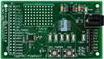
PAC-POWR607-EV Evaluation Board
The PAC-POWR607-EV evaluation board (Figure 1) allows the designer to quickly configure and evaluate the ispPAC-POWR607 device on a fully assembled printed-circuit board. The board supports a 32-pin QFN package,
pads for user I/O, a JTAG programming cable connector, LEDs and switches. JTAG programming signals can be
generated by using an ispDOWNLOAD® programming cable connected between the evaluation board and a PC’s
parallel (printer) port. Both analog and digital features of the ispPACPOWR607device can be easily configured
using PAC-Designer® software.
Figure 1. PAC-POWR607-EV Evaluation Board
Programming Interface
Lattice Semiconductor’s ispDOWNLOAD cable can be used to program the ispPAC-POWR607 device on the evaluation board. This cable plugs into a PC-compatible’s parallel port connector, and includes active buffer circuitry
inside its DB-25 connector housing. The other end of the ispDOWNLOAD cable terminates in an 8-pin 0.100” pitch
header connector, which plugs directly into a mating connector, (J3) provided on the PAC-POWR607-EV evaluation
board.
Important Note: The board must be un-powered when connecting, disconnecting, or reconnecting the ispDOWNLOAD Cable. Always connect the ispDOWNLOAD Cable's GND pin (black wire), before connecting any other JTAG
pins. Failure to follow these procedures can in result in damage to the ispPAC-POWR607 device and render the
board inoperable.
2
�ispPAC-POWR607
Evaluation Board User’s Guide
Lattice Semiconductor
Power Supply Considerations
The ispPAC-POWR607 device operates with analog and digital core power supplies of 3.3V, To simplify evaluation
work, the evaluation board was designed to operate from a single 4.5V to 9V power supply, which may be brought
in through a standard 5mm power plug (J2 - center tip positive). The evaluation board provides a linear regulator to
provide the appropriate operating voltages for the ispPACPOWR607 device, as well as reverse polarity protection.
The kit comes with a battery and cable that plugs into the connector at J2 and provides power with a 9V battery,
see Figure 2. If it is desired to test the current in the power down mode of the ispPAC-POWR607, the link between
pins 3 and 4 of J1 should be cut (please refer to Appendix A). Otherwise, approximately 2mA will be drawn when
the device is in power down mode.
Figure 2. 9V Battery Power Interface
Input/Output Connections
Connectors are provided for key functions and test points on this evaluation board, as shown In Figure 1. The JTAG
programming cable is connected to a header (J3) in the lower right corner of the board.
Access to the ispPAC-POWR607 device’s I/O pins is available along the left edge of the assembly, where a 2x17
block of pads (J1)supports the attachment of test probes or a ribbon-cable connector. In addition, there is an array
of 70 proto-type holes for interfacing.
Two momentary switches, S1 and S2, are provided on the evaluation board. They are connected to IN1_PWRDN
and IN2 respectively. Several LEDs are also provided on the evaluation board to indicate proper function and as
aids to debugging. LED D2 indicates that the on-board 3.3V supply is powered up. LED D3 is connected to the
ispPACPOWR607 device’s TDO line, and will briefly flash when downloading, indicating that download data has
made it to the device. Five LEDs are also provided on digital outputs OUT3 through OUT7 so that a user may easily
view the progress of Sequence, Monitor, Reset programs run on the evaluation board.
Demo Sequence and Reprogramming
This evaluation board is shipped from the factory pre-programmed with the “ispPAC_POWR607_LED_Blinker.PAC”
sequence from PAC-Designer’s library. The IN1_PWRDN button must be depressed in order t bring the ispPACPOWR607 device out of its power down mode. The programmed sequence will cause the LEDs to flash for about
six seconds, and then the device will revert to the power down mode.
In order to reprogram the ispPAC-POWR607, it must be brought out of power down mode. Thus, the IN1_PWRDN
button must be depressed immediately before beginning a download to the device from PAC-Designer or ispVM.
3
�ispPAC-POWR607
Evaluation Board User’s Guide
Lattice Semiconductor
Bill of Materials for the ispPAC-POWR607 Evaluation Board
Ref Des
Qty.
2
C1, C4
5
1
Description
Dig-Key # or Equivalent
10µF 10V Tant. SMD capacitor
478-1751-1-ND
C2, C3,C5,C6,C8
0.1µF SMD0603 ceramic capacitor
PCC1762CT-ND
D1
Diode Schottky 20V 1A SOD123Fl
MBR120VLSFT10SCT-ND
1
R1
1k resistor SMD 0805
311-1.0KACT-ND
1
D2
GREEN LED SMD 1206
160-1404-1-ND
6
D3, 4, 5, 6, 7, 8
RED LED SMD 1206
160-1405-1-ND
1
J2
2.5mm power connector
CP-102B-ND
1
RN1
Res Net 2k 14-pin SOIC
768-141-R2K-ND
2
R2, R3
10k resistor SMD 0805
311-10KACT-ND
2
R5, R6
4.7k resistor SMD 0805
311-4.7KACT-ND
1
J3
Header 36 pos .100 vert Gold Break into 8-pin used for JTAG
WM6736-ND
2
SW1, SW2
Momentary push-button switches
P10885SCT-ND
1
U1
ispPAC-POWR607
Lattice Semiconductor
1
U2
IC 3.3V LDO REG SOIC
296-2787-5-ND
1
N/A
PCB 2” by 3.5”
ispPAC-POWR607 Rev-2
Ordering Information
• Part Number: PAC-POWR607-EV
References
• ispPAC-POWR607 Data Sheet
Technical Support Assistance
Hotline: 1-800-LATTICE (North America)
+1-503-268-8001 (Outside North America)
e-mail: isppacs@latticesemi.com
Internet: www.latticesemi.com
Revision History
Date
Version
May 2007
01.0
Change Summary
Initial release.
© 2007 Lattice Semiconductor Corp. All Lattice trademarks, registered trademarks, patents, and disclaimers are as
listed at www.latticesemi.com/legal. All other brand or product names are trademarks or registered trademarks of
their respective holders. The specifications and information herein are subject to change without notice.
4
�5
A
B
C
D
5
4
TDO
5
TCK
TMS
TDI
R6
4.7k
R5
4.7k
HEADER 17X2
1
3
5
7
9
11
13
15
17
19
21
23
25
27
29
31
33
1
2
3
4
5
6
7
8
VCC
2
4
6
8
10
12
14
16
18
20
22
24
26
28
30
32
34
JTAG Interface
J3
IN_OUT7
IN_OUT6
IN_OUT5
IN_OUT4
IN_OUT3
IN2
IN1_PWRDN
HVOUT1
HVOUT2
VMON1
VMON2
VMON3
VMON4
VMON5
VMON6
4
100
100
VMON1
VMON2
VMON3
VMON4
VMON5
VMON6
TDI
TDO R7
TMS
TCK
R4
IN1_PWRDN
IN2
VCC is jumpered to 3.3V at pins 1 and 2 of J1 on the backside
of the board. To measure the device power down current, cut the
jumper trace on the backside of the board and connect an ammenter
between pins 1 and 2. In addition, cut the jumper on the backside
betweeen pins 3 and 4 of J1 to disconnect VCCJ. Replace with jumper
blocks for normal operation.
VCC
3.3V
J1
VCCJ
3
VCC
C7
50pF
18
14
19
15
29
28
2
3
5
6
7
10
3
C5
100n
TDI
TDO
TMS
TCK
IN1
IN2
21
4
13
HVOUT1
HVOUT2
VCCJ
C6
100n
Date:
Size
A
Title
27
26
23
22
20
30
31
IN_OUT3
IN_OUT4
IN_OUT5
IN_OUT6
IN_OUT7
HVOUT1
HVOUT2
2
Document Number
ispPAC-POWR0607 Evaluation Board
ispPAC-POWR0607
C8
100n
11
12
VCCJ
GNDA
IN/OUT3
IN/OUT4
IN/OUT5
IN/OUT6
IN/OUT7
ispPAC-POWR0607
VCCA
VCCJ
GNDD
VCCD
VMON1
VMON2
VMON3
VMON4
VMON5
VMON6
U1
VCC
2
Sheet
1
1
1
of
3
Rev
3
A
B
C
D
Lattice Semiconductor
ispPAC-POWR607
Evaluation Board User’s Guide
Appendix A. Schematics
The following figures comprise the schematics for the ispPAC-POWR607 evaluation board. Figure 3 shows the
device schematic and JTAG interface, while Figure 4 shows the on-board power-supply circuitry and the LED display.
Figure 3. ispPAC-POWR607 Device Schematic
�6
A
B
C
5
IN1_PWRDN
IN_OUT3
IN_OUT4
IN_OUT5
IN_OUT6
IN_OUT7
TDO
1
2
3
PWR JACK
R2
10k
2
4
3
4
SW4
IN1_PWRDN
(RED)
(RED)
(RED)
1
D11
OUT5
C2
100n
D10
OUT4
C1
10u
10V
3
4
D9
OUT3
MBR130p
D1
4
1
2
3
4
5
6
7
IN
IN
IN2
2k X 13
RN1
OUT
OUT
TPS77733
Regulator
U2
GND
Enb
1
2
D
J2
5
R3
10k
14
13
12
11
10
9
8
C3
100n
6
5
3
3
3.3V
2
1
C4
10u
10V
1k
R1
(RED)
D12
OUT6
3.3V
3
4
Date:
Size
A
Title
SW3
IN2
(RED)
D13
OUT7
D14
TDO
LEDs
2
Document Number
ispPAC-POWR0607 Evaluation Board
Power Supply and LEDs
(RED)
(GREEN)
D2
PWR
2
Sheet
3
1
1
of
3
Rev
3
A
B
C
D
Lattice Semiconductor
ispPAC-POWR607
Evaluation Board User’s Guide
Figure 4. Power Supply and LEDs
�