LX7176
1.65MHz 3A Synchronous Buck Converter
Production Datasheet
Description
Features
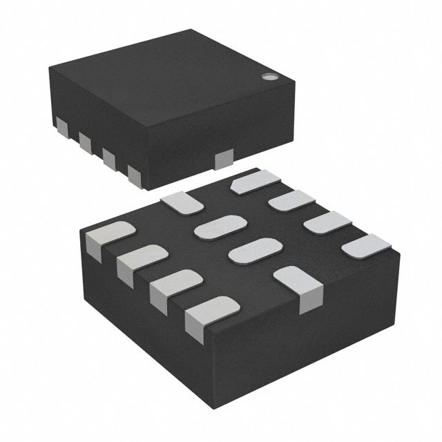
The LX7176 is a 3A step-down regulator with integrated
MOSFETs placed in a space saving QFN12 2mm x 2mm
package for today’s mobile devices. It uses an ultra fast,
constant frequency hysteretic control method and a
high switching frequency to minimize external filter
components while maintaining excellent regulation. The
LX7176 has a fixed 0.6V reference, Power Good, and
Enable pins. The LX7176 operates from 3.0V to 5.5V
rails.
0-3A Step-down Regulator
Cycle-by-cycle current limiting protects against overcurrent conditions. The LX7176 operates in hiccup mode
to further enhance the robustness of the converter for
heavy over-load or short-circuit faults and it
automatically recovers once the fault clears.
Enable and Power Good Function
Thermal protection shuts down the regulator under
over-temperature conditions. Over voltage conditions
will immediately shut off the output to protect against
permanent damage.
Operational Input Supply Voltage Range:
3.0V-5.5V (short durations to 6.5V)
Integrated PMOS and NMOS
Hysteretic Control Offers Best Transient
Response
PWM Switching at a Constant 1.65MHz
Input Under-voltage and Over-voltage
Protection
Internal Soft-start
Cycle-by-Cycle Over Current Protection
Hiccup Mode Protects Against Short Circuit
Faults
RoHS Compliant & Halogen Free
Applications
High Performance HDD
LCD TV
Notebook/Netbook
Server and Workstations
Video Cards
PoE Powered Devices Smart Phone
Figure 1: Typical Application Diagram with 0.9V VOUT
Copyright © 2012
Rev. 1.1a 1/28/2014
Microsemi
Analog Mixed Signal Group
One Enterprise Aliso Viejo, CA 92656 USA 1-800-713-4113, 1-949-380-6100, fax 1-949-215-4996
Page 1
�LX7176
1.65MHz 3A Synchronous Buck Converter
Production Datasheet
Other Typical Application Diagram
Figure 2. Typical Application with 1.8V VOUT
Pin Configuration and Pinout
•7176
YWWL
• Pin 1 Indicator, YWWL = Year/Week/Lot Code
RoHS / Pb-free Matte Tin Pin Finish
Figure 3: Pinout
Copyright © 2012
Rev. 1.1a 1/28/2014
Microsemi
Analog Mixed Signal Group
One Enterprise Aliso Viejo, CA 92656 USA 1-800-713-4113, 1-949-380-6100, fax 1-949-215-4996
Page 2
�LX7176
1.65MHz 3A Synchronous Buck Converter
Production Datasheet
Ordering Information
Ambient
Temperature
Type
Package
Part Number
0°C to 85°C
RoHS compliant, Pb-free
QFN 2x2mm 12L
LX7176CLQ
LX7176CLQ-TR
Packaging
Type
Bulk
Tape and Reel
Thermal Properties
Thermal Resistance(θJA)
QFN 2x2mm 12L
Typ
30
Units
°C/W
Note: The Jx numbers assume no forced airflow. Junction Temperature is calculated using TJ = TA + (PD x JA). In particular,
θJA is a function of the PCB construction. The stated number above is for a four-layer board in accordance with JESD-51
(JEDEC).
Pin Description
Pin Number
Pin Designator
Description
Supply Voltage – A capacitor is needed to prevent voltage spikes
from damaging the device. The capacitor return should be
connected directly to the PGND pin.
1
PVIN
2, 11
SW
3, 12
PGND
Power Ground – Power return.
4
AGND
Analog Ground – Quiet ground for control circuits.
5
NC
6
OUT
Output Voltage Sense Pin – This pin monitors the output voltage.
7
FB
Feedback – This pin is connected to an external resistor divider to
program the system output voltage.
8
EN
Enable – The device is enabled when this pin is held high.
9
PG
Power Good – Open Drain output that is pulled low when the FB is
outside the “good”range, during soft start, or during a fault
condition.
10
VIN
Internal control circuit supply voltage. Internal connection to PVIN.
Copyright © 2012
Rev. 1.1a 1/28/2014
Switch Output – This pin switches between PVIN and GND.
Leave pin unconnected.
Microsemi
Analog Mixed Signal Group
One Enterprise Aliso Viejo, CA 92656 USA 1-800-713-4113, 1-949-380-6100, fax 1-949-215-4996
Page 3
�LX7176
1.65MHz 3A Synchronous Buck Converter
Production Datasheet
Block Diagram
Figure 4: Block Diagram
Copyright © 2012
Rev. 1.1a 1/28/2014
Microsemi
Analog Mixed Signal Group
One Enterprise Aliso Viejo, CA 92656 USA 1-800-713-4113, 1-949-380-6100, fax 1-949-215-4996
Page 4
�LX7176
1.65MHz 3A Synchronous Buck Converter
Production Datasheet
Absolute Maximum Ratings
Performance is not necessarily guaranteed over this entire range. These are maximum stress ratings
only. Exceeding these ratings, even momentarily, can cause immediate damage, or negatively impact
long-term operating reliability.
Parameter
VIN, PVIN, EN, PG, OUT, FB to GND
SW to GND
SW to GND (Shorter than 50ns)
Maximum Junction Temperature
Storage Temperature
Peak Lead Soldering Temperature (40s, reflow)
Min
-0.3
-0.3
-2
-65
Max
7
7
7
150
150
260
Units
V
V
V
°C
°C
°C
Operating Ratings
Performance is generally guaranteed over this range as further detailed below under Electrical
Characteristics.
Parameter
Input Voltage
Output Voltage
Output Current
Ambient Temperature
Min
3.0
0.6
0
0
Max
5.5
3.3
3
85
Units
V
V
A
°C
Note: Corresponding Max Junction Temperature is 125°C
Copyright © 2012
Rev. 1.1a 1/28/2014
Microsemi
Analog Mixed Signal Group
One Enterprise Aliso Viejo, CA 92656 USA 1-800-713-4113, 1-949-380-6100, fax 1-949-215-4996
Page 5
�LX7176
1.65MHz 3A Synchronous Buck Converter
Production Datasheet
Electrical Characteristics
Unless otherwise specified, the following specifications apply over the operating ambient temperature
of 0°C ≤ TA ≤ 85°C except where otherwise noted with the following test conditions: PVIN = 5V. T J =
25°C, unless otherwise specified.
Symbol
VIN
IQ
ISLEEP
UVLO
UVLOHYST
Parameter
No Load Input
Current
Input Current at
Shutdown
Under Voltage
Rising Threshold
UVLO Hysteresis
OVPR
Over Voltage
Rising Threshold
OVPF
Over Voltage
Falling Threshold
VREF
VREF
TSS
Reference Voltage
VREF Slew Rate
THICCUP
Hiccup Time
Conditions
Min
Typ
ILOAD = 0, PWM,
VFB=0.75V
600
EN = low
0.1
VIN rising
PVIN falling
PVIN rising. Will also
trigger on
DV/DT > 1V/µs
PVIN falling
Max
Units
µA
3
µA
2.8
V
0.2
V
6.21
V
5.5
5.85
V
0.594
0.6
2
FB = 0.2V, does not
include soft start time
0.606
V
mV/µs
1.2
ms
0.1
%/V
-0.1
%/A
µA
FB
Line Regulation¹
Load Regulation¹
FB Input Current
VIN from 4.0V to 5.5V,
ILOAD = 1.0A
ILOAD = 0.5A to 2A
1
FBUVLO
FB Under Voltage
Threshold
VOUT below this
threshold will initiate a
hiccup sequence.
VOUT
Output Discharge
Resistance
EN = low
Copyright © 2012
Rev. 1.1a 1/28/2014
80%
80
200
Microsemi
Analog Mixed Signal Group
One Enterprise Aliso Viejo, CA 92656 USA 1-800-713-4113, 1-949-380-6100, fax 1-949-215-4996
VREF
1400
Ω
Page 6
�LX7176
1.65MHz 3A Synchronous Buck Converter
Production Datasheet
Symbol
Parameter
Conditions
Min
Typ
Max
Units
SW
RDSON_H
RDSON_L
OCP
TSH
TH
f
TOCP
EN
VIH
VIL
VH
III
PG
VPG90
VPG110
VPGHY
PGRDSON
High Side On
Resistance
Low Side On
Resistance
Rated Output
Current
Current Limit
Thermal
Shutdown
Threshold¹
Thermal
Shutdown
Hysteresis¹
PWM Switching
Frequency
OCP off time in
CCM
WRT rated current
1.2
IOUT = 5A
Input High
Input Low
Hysteresis
Input Current
PGOOD VOUT
Lower Threshold
PGOOD VOUT
Upper Threshold
Hysteresis
PGOOD Pull-down
Resistance
PGOOD Leakage
Current
140
35
mΩ
21
mΩ
3
A
170
200
150
°C
20
°C
1.65
2
MHz
360
ns
0.1
0.01
V
V
V
µA
1.1
0.4
VOUT rising, percentage
of VREF
VOUT falling,
percentage of VREF
Percentage of VREF
%
1
90
%
110
%
5
%
100
300
Ω
0
1
µA
¹ These parameters are not tested, but guaranteed by design and characterization.
Copyright © 2012
Rev. 1.1a 1/28/2014
Microsemi
Analog Mixed Signal Group
One Enterprise Aliso Viejo, CA 92656 USA 1-800-713-4113, 1-949-380-6100, fax 1-949-215-4996
Page 7
�LX7176
1.65MHz 3A Synchronous Buck Converter
Production Datasheet
Typical Performance Curves (Efficiency)
Figure 5: LX7176 Efficiency with 0.9V, 1.8V and 3.3V Output Voltage
Copyright © 2012
Rev. 1.1a 1/28/2014
Microsemi
Analog Mixed Signal Group
One Enterprise Aliso Viejo, CA 92656 USA 1-800-713-4113, 1-949-380-6100, fax 1-949-215-4996
Page 8
�LX7176
1.65MHz 3A Synchronous Buck Converter
Production Datasheet
Step Response(Load Current = 1A to 2.5A, Cout = 4*22μF)
CH2: VOUT, CH4: Load Current
Figure 6. VOUT = 0.9V, L = 2.2μH
CH2: VOUT, CH4: Load Current
Figure 7. VOUT = 1.8V, L = 4.9μH
CH2: VOUT, CH3: SW, CH4: Load Current
Figure 8.VOUT = 0.9V, L = 2.2μH
CH2: VOUT, CH3: SW, CH4: Load Current
Figure 9. VOUT = 1.8V, L = 4.9μH
Copyright © 2012
Rev. 1.1a 1/28/2014
Microsemi
Analog Mixed Signal Group
One Enterprise Aliso Viejo, CA 92656 USA 1-800-713-4113, 1-949-380-6100, fax 1-949-215-4996
Page 9
�LX7176
1.65MHz 3A Synchronous Buck Converter
Production Datasheet
CH2: VOUT, CH3: SW, CH4: Load Current
Figure 10. VOUT = 0.9V, L = 2.2μH
Copyright © 2012
Rev. 1.1a 1/28/2014
CH2: VOUT, CH3: SW, CH4: Load Current
Figure 11. VOUT = 1.8V, L = 4.9μH
Microsemi
Analog Mixed Signal Group
One Enterprise Aliso Viejo, CA 92656 USA 1-800-713-4113, 1-949-380-6100, fax 1-949-215-4996
Page 10
�LX7176
1.65MHz 3A Synchronous Buck Converter
Production Datasheet
Theory of Operation
Basic Operation
Over Current Protection
The LX7176 compares the FB voltage to an internal
reference, VREF. When FB is lower than VREF, the
upper switch turns on and the lower switch
turns
LX7166
off. When FB is higher than VREF, the upper switch
turns off and the lower switch turns on, VREF is
fixed at 0.6V. An internal ramp keeps FB constant
over a wide range of output capacitor values and
parasitic components (i.e. ESR, ESL). In addition, a
frequency control loop keeps the switching
frequency constant during continuous conduction
mode (CCM).
The LX7176 protects against all types of short circuit
conditions. Cycle by cycle over current protection
turns off the upper switch when the current exceeds
the OCP threshold. When this occurs, the upper
switch is kept off for about 360ns before being
allowed to turn on again. After startup, if FB drops
below the FB under voltage threshold, a hiccup
sequence will be initiated where both output
switches are shut off for 1.2ms before initiating
another soft start. This protects against a crowbar
short circuit. The FB under voltage detection is not
active during startup.
Startup
The LX7176 is enabled when EN is high and PVIN
rises above the UVLO threshold. At start up, VREF
ramps up from 0V to 0.6V. While VREF ramps;
PGOOD (PG Pin) is held low. At the end of the
ramp time, PG is allowed to go high after FB has
reached the PGOOD rising threshold.
Application Information
Output Components Selection
VOUT
Inductor (L1)
0.9V
1.8V
3.3V
2.2μH
4.9μH
1.0μH
Copyright © 2012
Rev. 1.1a 1/28/2014
Upper Feedback
Resistor (R4)
100kΩ
200kΩ
453kΩ
Lower Feedback
Resistor (R5)
200kΩ
100kΩ
100kΩ
Output Capacitor
(C2 & C3)
4x22μF
4x22μF
4x22μF
Microsemi
Analog Mixed Signal Group
One Enterprise Aliso Viejo, CA 92656 USA 1-800-713-4113, 1-949-380-6100, fax 1-949-215-4996
Page 11
�LX7176
1.65MHz 3A Synchronous Buck Converter
Production Datasheet
Package Dimensions
QFN 2x2mm 12L Package
D2
D
L
10
b
9
1
8
2
7
3
E
e
6
4
5
Top View
b
A
A3
Bottom View
Side View
Dim
A
A3
B
D
D2
E
e
L
MILLIMETERS
MIN
MAX
0.80
1.00
0.20 REF
0.20
0.30
2.0 BSC
0.50
2.0 BSC
0.50 REF
0.30
0.45
INCHES
MIN
MAX
0.031
0.039
0.008 REF
0.008
0.012
0.078 BSC
0.020
0.078 BSC
0.020 REF
0.012
0.018
Note:
1. Dimensions do not include mold flash or
protrusions; these shall not exceed 0.155mm
(.006”) on any side. Lead dimension shall not
include solder coverage.
2. Dimensions are in millimeters, inches for
reference only.
PRODUCTION DATA – Information contained in this document is proprietary to Microsemi
and is current as of publication date. This document may not be modified in any way without
the express written consent of Microsemi. Product processing does not necessarily include
testing of all parameters. Microsemi reserves the right to change the configuration and
performance of the product and to discontinue product at any time.
Copyright © 2012
Rev. 1.1a 1/28/2014
Microsemi
Analog Mixed Signal Group
One Enterprise Aliso Viejo, CA 92656 USA 1-800-713-4113, 1-949-380-6100, fax 1-949-215-4996
Page 12
�