A
MICROSEMI
����������
COMPANY
LX8630-xx
3A BiCMOS Very Low Dropout Regulators
P R O D UC TI O N D ATA S HEET
���������
The LX8630 family are positive very They are low dropout regulators. designed to provide a power supply for very low headroom applications, such as 3.3V – 2.5V. BiCMOS technology allows an effective series pass element resistance, RDS(ON) of 150m� ������
�
� �
� ��� dropout voltage of 450mV at 3A. Low Quiescent Current and LogicControlled Shutdown help conserve battery life and increase system efficiency. Typical quiescent current is under 400�A irrespective of load current, while the
Shut���
�����
� � �
�
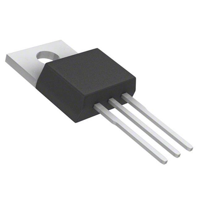
����� ��� device will enter shutdown mode when the SHDN pin is pulled low. Thermal and Short-Circuit Current Limiting: the LX8630 limits the current when the output is shorted, protecting the sensitive load circuits. The device will also turn off if the junction temperature exceeds 150° Available in Popular TO-220 and TO-263 Power Packages: adjustable versions have five leads, and fixed output voltage devices are supplied in three lead packages.
��
��������
� Dropout Voltage Typically �
W W W . Microsemi . COM
� �
� �
450mV at 3A and 50mV at 10mA Low Quiescent Current, Typically Under 400µA, irrespective of Load Shutdown Current 10µA Adjustable Output Version in 5-Pin TO-220 & TO-263 Packages Low Reverse Leakage Current Short-Circuit and Thermal Shutdown Protection
IMPORTANT: For the most current data, consult MICROSEMI’s website: http://www.microsemi.com
���������
����
���� � ���������
����
�����
� 3.3V & 2.5V Supplies for
Memory, Microprocessors, Clock Circuits, Etc. � Portable Equipment
�� ���� ���������
LX8 630-xx S im plified B lock D iagra m
V IN
C urrent Lim it R eference C urrent C harge P um p RA
V O UT
A D J*
1.25V
+
RB
SHDN*
V IN /2
-
GND
RA
RB 25K 25K
R everse V oltage Sense
LX 8630-00
25K 41K
T herm al S hutdown
* A djustable 5 lead ve rsion only
LX 8630-25 LX 8630-33
LX8630-XX LX8630-XX
������� �
� ��
�
Output TA (°C) Voltage 3.3 0 to 125 2.5 ADJ(00) Plastic TO-220 P 3-Pin LX8630-33CP LX8630-25CP -
P
Plastic TO-220 5-Pin LX8630-00CP
DD
Plastic TO-263 3-Pin LX8630-33CDD LX8630-25CDD -
DD
Plastic TO-263 5-Pin LX8630-00CDD
Note: Available in Tape & Reel. Append the letter “T” to the part number. (i.e. LX8630-33CDDT)
Copyright © 2000 Rev. 1.0a,2000-11-28
Microsemi
Linfinity Microelectronics Division 11861 Western Avenue, Garden Grove, CA. 92841, 714-898-8121, Fax: 714-893-2570
Page 1
�A
MICROSEMI
����������
COMPANY
LX8630-xx
3A BiCMOS Very Low Dropout Regulators
P R O D UC TI O N D ATA S HEET
��� ���� ������� ����
��
Input Voltage (VIN) ......................................................................................................6.5V SHDN Pin..............................................................................................-0.3V to VIN +0.3V Operating Junction Temperature Plastic (P & DD Packages)................................................................................... 150 °C Storage Temperature Range ........................................................................-65 °C to 150°C Lead Temperature (Soldering, 10 seconds) ............................................................... 300°C
Note: Exceeding these ratings could cause damage to the device. All voltages are with respect to Ground. Currents are positive into, negative out of specified terminal.
� ������ ��
�� �������
TAB is GND
VOUT GND VIN
W W W . Microsemi . COM
3
2
1
DD PACKAGE (3-PIN)
(Top View)
������� ����
PLASTIC TO-220 3-PIN THERMAL RESISTANCE-JUNCTION TO TAB , θJT THERMAL RESISTANCE-JUNCTION TO AMBIENT, θJA PLASTIC TO-220 5-PIN THERMAL RESISTANCE-JUNCTION TO TAB, θJT THERMAL RESISTANCE-JUNCTION TO AMBIENT, θJA PLASTIC TO-263 3-PIN THERMAL RESISTANCE-JUNCTION TO TAB, θJT THERMAL RESISTANCE-JUNCTION TO AMBIENT, θJA
T A B is G N D
V OUT ADJ GND SHDN V IN
5
P
4
2.1°C/W 60°C/W
3 2 1
D D P A C K A G E ( 5-P IN )
P
(T op V iew)
2.1°C/W 60°C/W
T A B is G N D
DD
5 4
VOUT ADJ GND SHDN V IN
2.1°C/W 60°C/W
3 2 1
P P A C K A G E ( 5-P IN )
(Top V iew)
DD PLASTIC TO-263 5-PIN THERMAL RESISTANCE-JUNCTION TO TAB, θJT THERMAL RESISTANCE-JUNCTION TO AMBIENT, θJA
2.1°C/W 60°C/W
TAB is GND
3
Junction Temperature Calculation: TJ = TA + (PD x θJA). The θJA numbers are guidelines for the thermal performance of the device/pc-board system. All of the above assume no ambient airflow. • θJA can be improved with package soldered to 0.5IN2 copper area over backside ground plane or internal power plane. θJA can vary from 20°C/W to > 40°C/W depending on mounting technique. See table below for thermal resistance guidelines:
VOUT GND VIN
2
1
P PACKAGE (3-PIN)
(Top View)
Copper Area (Topside)*
2.5 sq” (1613mm2) 1.0 sq” (645 mm2) 0.17 sq” (110 mm2)
Copper Area (Backside)*
2.5 sq” (1613mm2) 2.5 sq” (1613mm2) 2.5 sq” (1613mm2)
Board Area
2.5 sq” (1613mm2) 2.5 sq” (1613mm2) 2.5 sq” (1613mm2)
Thermal Resistance (θJA)
25°C/W 27°C/W 35°C/W
PACKAGE DATA PACKAGE DATA
*Tab of device attached to topside copper
Copyright © 2000 Rev. 1.0a,2000-11-28
Microsemi
Linfinity Microelectronics Division 11861 Western Avenue, Garden Grove, CA. 92841, 714-898-8121, Fax: 714-893-2570
Page 2
�A
MICROSEMI
����������
COMPANY
������ ��� ��� ���������� �� �� ����������� ��
LX8630-xx
3A BiCMOS Very Low Dropout Regulators
P R O D UC TI O N D ATA S HEET
�
��
���
��
���
�� ��
���������
�
��� �
����
W W W . Microsemi . COM
VIN VOUT GND ADJ SHDN
Positive supply input for the regulator. Bypass to GND with at source is further than 1 inch from the device.
����� ���
�� ��
���� ��� ����������� �� ������
����� �� !"#
��� �� ����� $%
�������� ���� �� ��� ��&����� ���
regulation, rather it is needed for transient response. Size your output capacitor to meet the transient loading requirement. If you have a very dynamic load, a larger capacitor will improve the response to these load steps. Reference ground. The input and output bypass capacitors should be connected to this pin. The tab on the TO220 and TO-263 packages along with the ground pin are also used for heatsinking the device. Feedback pin for the regulator. For the LX8630-00, the output voltage can be set by two external resistors with the following relationship: VOUT = 1.25V * (1+RA/RB) where RA is the resistor connected between VOUT and ADJ, RB is the resistor connected between ADJ and GND pin. Shutdown pin. For the LX8630-00, this pin has a threshold of about V IN/2, it should be actively pulled high to enable the regulator. This can be accomplished with a resistive pull-up. When low, it turns off the regulator and puts the device in a low current shutdown state.
�
����� ���������
V IN
1
IN
OUT
5
V OUT RA
C IN
L X 8630-00
SHDN
2
GND
3
ADJ
4
C OUT V REF RB
V OUT = V REF 1 +
RA RB
PIN DESCRIPTION
FIGURE 1
– Typical Application
Copyright © 2000 Rev. 1.0a,2000-11-28
Microsemi
Linfinity Microelectronics Division 11861 Western Avenue, Garden Grove, CA. 92841, 714-898-8121, Fax: 714-893-2570
Page 3
�A
MICROSEMI
����������
COMPANY
LX8630-xx
3A BiCMOS Very Low Dropout Regulators
P R O D UC TI O N D ATA S HEET
��� ���
��� ������
� �
����
� �
�������
�
W W W . Microsemi . COM
� �����
�
��
������
PARAMETER
INPUT VOLTAGE LOAD CURRENT (WITH ADEQUATE HEATSINKING) INPUT CAPACITOR (VIN TO GND) OUTPUT CAPACITOR (VOUT TO GND)
SYMBOL
VIN
MIN.
3.0 0.01 10 22
TYP.
MAX.
5.5 3
UNITS
V A
100 220*
�� ��
* Size your output capacitor to meet the transient loading requirement. If you have a very dynamic load, a larger capacitor will improve the response to these load steps (see charts 2&3) (Unless otherwise specified, the following specifications apply over the operating ambient temperatures for the LX8630-xxC with 0°C ≤ TA ≤ 125°C; VIN = VOUT + 1.5V; IOUT = 10mA; CIN = 10
' (OUT ) ��
' *J = TA. Test conditions: Low duty cycle pulse testing techniques are used which maintains junction and case temperatures equal to the ambient temperature.) Parameter Symbol Test Conditions LX8630-xx Typ Max Units
���������� ���������������
Min
�
LX8630-33 FIXED 3.3V, 3A Output Voltage Line Regulation Load Regulation Dropout Voltage (VDO = VIN - VOUT) VOUT VREG IREG VDO TJ = 25°C Over Temperature VIN = 3.9V to 5.5V IOUT = 10mA to 3 A IOUT = 3A, ��OUT = -1% IOUT = 1.5A, ��OUT = -1% IOUT = 10mA, ��OUT = -1% Short Circuit Current Quiescent Current Reverse Leakage Current ISC IQ IREV VOUT = 0V IOUT = 10mA to 3A 0V < VIN < VOUT, VOUT < 3.4V (at VOUT) 0V < VIN < VOUT, VOUT < 3.4V (at VIN) -50 3.25 3.22 2 18 0.4 0.3 0.05 5 400 50 0 3.3 3.35 3.38 8 40 0.6 0.4 0.15 6.5 600 650 A V V mV mV
�� ��
mA
�
LX8630-25 FIXED 2.5V, 3A Output Voltage Line Regulation Load Regulation VOUT VREG IREG TJ = 25°C Over Temperature VIN = 3.1V to 5.5V IOUT = 10mA to 3 A IOUT = 3A, ��OUT = -1%, TJ = 85°C Dropout Voltage (VDO = VIN - VOUT) VDO IOUT = 1.5A, ��OUT = -1% IOUT = 10mA, ��OUT = -1% Short Circuit Current Quiescent Current Reverse Leakage Current ISC IQ IREV VOUT = 0V IOUT = 10mA to 3A 0V < VIN < VOUT, VOUT < 2.6V (at VOUT) 0V < VIN < VOUT, VOUT < 2.6V (at VIN) -50 2.46 2.44 2.5 2.5 2 14 0.4 0.3 0.05 5 400 50 0 2.54 2.56 6 30 0.6 0.45 0.15 6.5 600 650 A V mV mV V
ELECTRICALS ELECTRICALS
�� ��
mA
Copyright © 2000 Rev. 1.0a,2000-11-28
Microsemi
Linfinity Microelectronics Division 11861 Western Avenue, Garden Grove, CA. 92841, 714-898-8121, Fax: 714-893-2570
Page 4
�A
MICROSEMI
����������
COMPANY
LX8630-xx
3A BiCMOS Very Low Dropout Regulators
P R O D UC TI O N D ATA S HEET
���������� ��������������� ��
��
����
Parameter Symbol Test Conditions LX8630-xx Min Typ Max Units
W W W . Microsemi . COM
�
LX8630-00 ADJUSTABLE OUTPUT, 3A Reference Voltage Line Regulation Load Regulation VREF VREG IREG TJ = 25°C Over Temperature VIN = (VO + 0.6V) to 5.5V @ ADJ Pin (Note 1) IOUT = 10mA to 3A @ ADJ Pin IOUT = 3A, ��OUT = -1%, TJ = 85°C Dropout Voltage VDO IOUT = 1.5A, ��OUT = -1% IOUT = 10mA, ��OUT = -1% Short Circuit Current Quiescent Current IQ Quiescent Current in Shutdown Reverse Leakage Current Bias Current at ADJ Pin Shutdown Threshold SHDN Bias Current Note 1: VIN min.���� IREV IBIAS VSHDN ISHDN VSHDN falling VSHDN rising VSHDN < 0.8V VSHDN = 3V 0.8 VIN= 4.8V; VSHDN


 工商网监
湘ICP备2023018690号
工商网监
湘ICP备2023018690号
