MP5094
Dual-Channel 12V/5V Current-Limit Switch with Output
Over-Voltage Clamp in Small 3x3mm TSOT23-8 Package
DESCRIPTION
FEATURES
The MP5094 is a protection device designed to
protect circuitry on the output from transients on
the input. The MP5094 also protects the input
from undesired shorts and transients coming
from the output. The MP5094 is a small RDS(ON),
low quiescent current, dual-channel, currentlimited switch.
During start-up, the inrush current is limited by
limiting the slew rate at the output. The slew
rate is controlled by a capacitor at the SS pin.
The maximum load at the output is currentlimited. The magnitude of the current limit is
fixed internally.
The output voltage is limited by an output overvoltage protection (OVP) function.
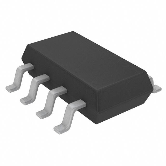
The MP5094 is available in a space-saving, 8pin, TSOT23 (3mmx3mm) package.
Integrated 5V, 12V Input Dual E-Fuse
24V 100ms Maximum Surge Input Voltage
Tolerance for 12V Bus
16V 100ms Maximum Surge Input Voltage
Tolerance for 5V Bus
Integrated Dual-Channel Current-Limit
Switch
50mΩ/30mΩ Low RDS(ON) for 12V Bus/5V
Bus Current-Limit Switch
110μA Typical Low Quiescent Current for
12V Bus/5V Bus
Adjustable Soft-Start Time
Fixed 4A/2.95A Trip/Hold Current Limit for
12V Bus
Fixed 3A/2.18A Trip/Hold Current Limit for
5V Bus
Over-Current Protection (OCP) Hiccup
Latch-Off Thermal Shutdown
Available in a TSOT23-8 Package
APPLICATIONS
Hard Disk Drives
Solid-State Drives
Hot Swap
All MPS parts are lead-free, halogen-free, and adhere to the RoHS
directive. For MPS green status, please visit the MPS website under
Quality Assurance. “MPS”, the MPS logo, and “Simple, Easy Solutions” are
trademarks of Monolithic Power Systems, Inc. or its subsidiaries.
TYPICAL APPLICATION
MP5094 Rev. 1.0
3/15/2019
www.MonolithicPower.com
MPS Proprietary Information. Patent Protected. Unauthorized Photocopy and Duplication Prohibited.
© 2019 MPS. All Rights Reserved.
1
�MP5094 – DUAL-CHANNEL CURRENT-LIMITED SWITCH
ORDERING INFORMATION
Part Number*
MP5094GJ
Package
TSOT23-8 (3mmx3mm)
Top Marking
See Below
* For Tape & Reel, add suffix –Z (e.g. MP5094GJ–Z).
TOP MARKING
AYU: Product code of MP5094GJ
Y: Year code
PACKAGE REFERENCE
TOP VIEW
TSOT23-8 (3mmx3mm)
MP5094 Rev. 1.0
3/15/2019
www.MonolithicPower.com
MPS Proprietary Information. Patent Protected. Unauthorized Photocopy and Duplication Prohibited.
© 2019 MPS. All Rights Reserved.
2
�MP5094 – DUAL-CHANNEL CURRENT-LIMITED SWITCH
PIN FUNCTIONS
Pin #
Name
1
VCC1
2
SS1
3
SS2
4
VCC2
5
6
VOUT2
GND
7
EN
8
VOUT1
Description
Supply voltage of channel 1. The channel 1 typical input voltage is 12V. Use a
ceramic capacitor to decouple the input rail. Connect VCC1 using a wide PCB trace.
Channel 1 soft-start pin. Connect a capacitor from SS1 to ground to set the soft-start
time.
Channel 2 soft-start pin. Connect a capacitor from SS2 to ground to set the soft-start
time.
Supply voltage of channel 2. The channel 2 typical input voltage is 5V. Use a
ceramic capacitor to decouple the input rail. Connect VCC2 using a wide PCB trace.
Output terminal of channel 2.
System ground.
Enable pin for channel 1 and channel 2. EN is a digital input that turns the
regulator on or off. Float EN or drive EN low to turn on the regulator. Drive EN high
to turn off the regulator.
Output terminal of the channel 1.
ABSOLUTE MAXIMUM RATINGS (1)
VCC1, VOUT1 ................................ -0.3V to 22V
Input voltage transient (Ch1 100ms) ............ 24V
VCC2, VOUT2 ................................ -0.3V to 15V
Input voltage transient (Ch2 100ms) ............ 16V
All other pins ................................... -0.3V to +5V
Junction temperature ................-40°C to +150°C
Lead temperature...................................... 260°C
Continuous power dissipation (TA = +25°C) (2)
TSOT23-8 (3mmx3mm) ............................ 1.89W
Recommended Operating Conditions (3)
Ch1 continuous supply voltage... 10.2V to 14.5V
Ch2 continuous supply voltage....... 4.6V to 5.5V
Operating junction temp. (TJ) ....-40°C to +125°C
MP5094 Rev. 1.0
3/15/2019
Thermal Resistance
θJA
θJC
TSOT23-8
EV5094-J-00A (4) ................... 66 ...... 23 ... °C/W
JESD51-7 (5) ......................... 100 ..... 55 ... °C/W
NOTES:
1) Exceeding these ratings may damage the device.
2) The maximum allowable power dissipation is a function of the
maximum junction temperature TJ (MAX), the junction-toambient thermal resistance θJA, and the ambient temperature
TA. The maximum allowable continuous power dissipation of
EV5094-J-00A board at any ambient temperature is
calculated by PD (MAX) = (TJ (MAX)-TA)/θJA. Exceeding the
maximum allowable power dissipation produces an excessive
die temperature, causing the regulator to go into thermal
shutdown. Internal thermal shutdown circuitry protects the
device from permanent damage. Here, the max power of the
TSOT23-8 is given by θJA on EV5094-J-00A.
3) The device is not guaranteed to function outside of its
operating conditions.
4) Measured on EV5094-J-00A, 2-layer PCB, 54mmx46mm.
5) The value of θJA given in this table is only valid for comparison
with other packages and cannot be used for design purposes.
These values were calculated in accordance with JESD51-7
and simulated on a specified JEDEC board. They do not
represent the performance obtained in an actual application.
www.MonolithicPower.com
MPS Proprietary Information. Patent Protected. Unauthorized Photocopy and Duplication Prohibited.
© 2019 MPS. All Rights Reserved.
3
�MP5094 – DUAL-CHANNEL CURRENT-LIMITED SWITCH
ELECTRICAL CHARACTERISTICS
VIN1 = 12V, VIN2 = 5V, COUT1 = COUT2 = 10μF, TJ = -40°C + 125°C
+25°C unless otherwise noted.
Parameter
Supply Current
Symbol
IQ_CH1
Quiescent current
IQ_CH2
Off-state leakage current
Power MOSFET
IOFF
RDS(ON)_CH1
On resistance
RDS(ON)_CH2
Tdelay_CH1
Turn-on delay (7)
Tdelay_CH2
(6)
, typical value is tested at TJ =
Condition
Output over-voltage response
time (7)
tOUT_OV_CH2
Typ
V EN = low
V EN = high
V EN = low
V EN = high
VIN = 14V, V EN = 2V
110
10
110
6.5
TJ = 25°C
TJ = 125°C
TJ = 25°C
TJ = 125°C
V EN = 0V to Vo begins
ramping up with a 3A load
resistor
V EN = 0V to Vo begins
ramping up with a 2A load
resistor
50
Under-/Over-Voltage Protection (UVP, OVP)
VUVLO_CH1
Under-voltage lockout rising
threshold
VUVLO_CH2
VUVLOHYS_CH1
UVLO hysteresis
VUVLOHYS_CH2
VOVLO_CH1
Output over-voltage clamp
voltage
VOVLO_CH2
tOUT_OV_CH1
Min
Max
Units
1
μA
μA
μA
μA
μA
70
30
50
9.2
4.1
14.5
5.5
COUT = 10µF, add a 30Ω load
resistor, VIN1 = 12V to
18V/10µs
COUT = 10µF, add a 10Ω load
resistor, VIN2 = 5V to 7V/10µs
mΩ
mΩ
mΩ
mΩ
690
μs
690
μs
9.7
4.4
800
1.7
15
5.7
10.2
4.6
15.5
6.0
V
V
mV
V
V
V
2
μs
2
μs
Current Limit
Current limit at normal
operation
Current limit response time (7)
Secondary current limit (7)
MP5094 Rev. 1.0
3/15/2019
ILimit_NO_CH1_TRIP
ILimit_NO_CH2_TRIP
ILimit_SC_CH1_Hold
ILimit_SC_CH2_Hold
tCL_CH1
tCL_CH2
ILimitH_CH1
ILimitH_CH2
3.6
2.65
2.7
1.95
4
2.95
3
2.18
15
15
8
8
www.MonolithicPower.com
MPS Proprietary Information. Patent Protected. Unauthorized Photocopy and Duplication Prohibited.
© 2019 MPS. All Rights Reserved.
4.4
3.25
3.3
2.4
A
A
A
A
μs
μs
A
A
4
�MP5094 – DUAL-CHANNEL CURRENT-LIMITED SWITCH
ELECTRICAL CHARACTERISTICS (continued)
VIN1 = 12V, VIN2 = 5V, COUT1 = COUT2 = 10μF, TJ = -40°C + 125°C
+25°C unless otherwise noted.
Parameter
Enable
Symbol
EN falling threshold
V EN _Falling
Condition
(6)
, typical value is tested at TJ =
Min
Typ
Max
Units
EN hysteresis
V EN _HYS
250
mV
EN pull-down resistor
R EN _PD
280
KΩ
Soft Start
ISS_CH1
ISS_CH2
SS current
OTP
Thermal shutdown (7)
TSD
4
4
5.5
5.5
155
7
7
μA
μA
°C
NOTES:
6) Not tested in production, guaranteed by over-temperature correlation.
7) Guaranteed by design and engineering sample characterization.
MP5094 Rev. 1.0
3/15/2019
www.MonolithicPower.com
MPS Proprietary Information. Patent Protected. Unauthorized Photocopy and Duplication Prohibited.
© 2019 MPS. All Rights Reserved.
5
�MP5094 – DUAL-CHANNEL CURRENT-LIMITED SWITCH
TYPICAL PERFORMANCE CHARACTERISTICS
VIN1 = 12V, VIN2 = 5V, VEN = float, TA = 25°C, unless otherwise noted.
Current Limit vs. Input Voltage (12V
E-Fuse)
Current Limit vs. Input Voltage (5V EFuse)
5
4
4.5
3.5
CURRENT LIMIT (A)
CURRENT LIMIT (A)
4
3.5
3
2.5
2
1.5
1
Trip
Hold
0.5
0
3
2.5
2
1.5
1
0
10 10.5 11 11.5 12 12.5 13 13.5 14
4.5 4.6 4.7 4.8 4.9
5
5.1 5.2 5.3 5.4 5.5
INPUT VOLTAGE (V)
INPUT VOLTAGE (V)
Quiescent Current vs. Input Voltage
(12V E-Fuse)
Quiescent Current vs. Input Voltage
(5V E-Fuse)
140
140
QUIESCENT CURRENT (µA)
QUIESCENT CURRENT (µA)
Trip
Hold
0.5
120
100
80
60
40
20
0
10
11
12
13
INPUT VOLTAGE (V)
14
120
100
80
60
40
20
0
15
4.5 4.6 4.7 4.8 4.9
5
5.1 5.2 5.3 5.4 5.5
INPUT VOLTAGE (V)
Shutdown Current vs. Input Voltage
(12V E-Fuse)
Shutdown Current vs. Input Voltage
(5V E-Fuse)
V EN = 3.3V
50
45
45
SHUTDOWN CURRENT (µA)
SHUTDOWN CURRENT (µA)
V EN = 3.3V
50
40
35
30
25
20
15
10
5
0
40
35
30
25
20
15
10
5
0
10
11
12
13
INPUT VOLTAGE (V)
MP5094 Rev. 1.0
3/15/2019
14
15
4.5 4.6 4.7 4.8 4.9
5
5.1 5.2 5.3 5.4 5.5
INPUT VOLTAGE (V)
www.MonolithicPower.com
MPS Proprietary Information. Patent Protected. Unauthorized Photocopy and Duplication Prohibited.
© 2019 MPS. All Rights Reserved.
6
�MP5094 – DUAL-CHANNEL CURRENT-LIMITED SWITCH
TYPICAL PERFORMANCE CHARACTERISTICS (continued)
VIN1 = 12V, VIN2 = 5V, VEN = float, TA = 25°C, unless otherwise noted.
VIN UVLO Rising/Falling Threshold
vs. Temperature (12V E-Fuse)
VIN UVLO Rising/Falling Threshold vs.
Temperature (5V E-Fuse)
TA = -40°C to +125°C
10
5
9.8
4.5
9.6
9.4
9.2
9
8.8
8.6
8.4
UVLO_Rising
8.2
UVLO_Falling
8
-40 -20
0
20
40
60
80 100 120 140
TEMPERATURE (˚C)
INPUT VOLTAGE (V)
INPUT VOLTAGE (V)
TA = -40°C to +125°C
4
3.5
3
2.5
2
1.5
1
UVLO_Rising
0.5
UVLO_Falling
0
-40 -20
0
20
40
60
80 100 120 140
TEMPERATURE (˚C)
EN Rising/Falling Threshold vs.
Temperature
TA = -40°C to +125°C
ENABLE VOLTAGE (V)
1.6
1.4
1.2
1
0.8
EN_Rising
0.6
EN_Falling
0.4
-40 -20
0
20
40
60
80 100 120 140
TEMPERATURE (˚C)
MP5094 Rev. 1.0
3/15/2019
www.MonolithicPower.com
MPS Proprietary Information. Patent Protected. Unauthorized Photocopy and Duplication Prohibited.
© 2019 MPS. All Rights Reserved.
7
�MP5094 – DUAL-CHANNEL CURRENT-LIMITED SWITCH
TYPICAL PERFORMANCE CHARACTERISTICS (continued)
VIN1 = 12V, VIN2 = 5V, VEN = float, TA = 25°C, unless otherwise noted.
Start-Up through Input Voltage (12V
E-Fuse)
Start-Up through Input Voltage (5V
E-Fuse)
IOUT1 = 0A
IOUT2 = 0A
CH1: VOUT1
5V/div.
CH1: VOUT2
2V/div.
CH2: VIN1
10V/div.
CH2: VIN2
5V/div.
CH4: IOUT1
2A/div.
CH4: IOUT2
2A/div.
5ms/div.
5ms/div.
Start-Up through Input Voltage (12V
E-Fuse)
Start-Up through Input Voltage (5V
E-Fuse)
IOUT1 = 3A
IOUT2 = 2A
CH1: VOUT1
5V/div.
CH1: VOUT2
2V/div.
CH2: VIN1
10V/div.
CH2: VIN2
5V/div.
CH4: IOUT1
2A/div.
CH4: IOUT2
2A/div.
5ms/div.
2ms/div.
Start-Up through Input Voltage (12V
E-Fuse)
Start-Up through Input Voltage (5V
E-Fuse)
IOUT1 = 0A, COUT1 = 1000μF
IOUT2 = 0A, COUT2 = 1000μF
CH1: VOUT1
5V/div.
CH1: VOUT2
2V/div.
CH2: VIN1
10V/div.
CH2: VIN2
5V/div.
CH4: IOUT1
2A/div.
CH4: IOUT2
2A/div.
5ms/div.
MP5094 Rev. 1.0
3/15/2019
5ms/div.
www.MonolithicPower.com
MPS Proprietary Information. Patent Protected. Unauthorized Photocopy and Duplication Prohibited.
© 2019 MPS. All Rights Reserved.
8
�MP5094 – DUAL-CHANNEL CURRENT-LIMITED SWITCH
TYPICAL PERFORMANCE CHARACTERISTICS (continued)
VIN1 = 12V, VIN2 = 5V, VEN = float, TA = 25°C, unless otherwise noted.
Shutdown through Input Voltage
(12V E-Fuse)
Shutdown through Input Voltage (5V
E-Fuse)
IOUT1 = 0A
IOUT2 = 0A
CH1: VOUT1
5V/div.
CH1: VOUT2
2V/div.
CH2: VIN1
10V/div.
CH2: VIN2
5V/div.
CH4: IOUT1
2A/div.
CH4: IOUT2
2A/div.
20ms/div.
10ms/div.
Shutdown through Input Voltage
(12V E-Fuse)
Shutdown through Input Voltage (5V
E-Fuse)
IOUT1 = 3A
IOUT2 = 2A
CH1: VOUT1
5V/div.
CH1: VOUT2
2V/div.
CH2: VIN1
10V/div.
CH2: VIN2
5V/div.
CH4: IOUT1
2A/div.
CH4: IOUT2
2A/div.
1ms/div.
2ms/div.
Start-Up through Enable (5V E-Fuse)
Start-Up through Enable (12V EFuse)
IOUT2 = 0A
IOUT1 = 0A
CH1: VOUT1
5V/div.
CH1: VOUT2
2V/div.
CH2: VIN1
10V/div.
CH3: VEN
2V/div.
CH2: VIN2
5V/div.
CH3: VEN
2V/div.
CH4: IOUT1
2A/div.
CH4: IOUT2
2A/div.
5ms/div.
MP5094 Rev. 1.0
3/15/2019
5ms/div.
www.MonolithicPower.com
MPS Proprietary Information. Patent Protected. Unauthorized Photocopy and Duplication Prohibited.
© 2019 MPS. All Rights Reserved.
9
�MP5094 – DUAL-CHANNEL CURRENT-LIMITED SWITCH
TYPICAL PERFORMANCE CHARACTERISTICS (continued)
VIN1 = 12V, VIN2 = 5V, VEN = float, TA = 25°C, unless otherwise noted.
Start-Up through Enable (5V E-Fuse)
Start-Up through Enable (12V EFuse)
IOUT2 = 2A
IOUT1 = 3A
CH1: VOUT1
5V/div.
CH1: VOUT2
2V/div.
CH2: VIN1
10V/div.
CH3: VEN
2V/div.
CH4: IOUT1
2A/div.
CH2: VIN2
5V/div.
CH3: VEN
2V/div.
CH4: IOUT2
2A/div.
5ms/div.
5ms/div.
Start-Up through Enable (12V EFuse)
Start-Up through Enable (5V E-Fuse)
IOUT2 = 0A, COUT2 = 1000μF
IOUT1 = 0A, COUT1 = 1000μF
CH1: VOUT1
5V/div.
CH1: VOUT2
2V/div.
CH2: VIN1
10V/div.
CH3: VEN
2V/div.
CH2: VIN2
5V/div.
CH3: VEN
2V/div.
CH4: IOUT2
2A/div.
CH4: IOUT1
2A/div.
5ms/div.
5ms/div.
Shutdown through Enable (12V EFuse)
Shutdown through Enable (5V EFuse)
IOUT1 = 0A
IOUT2 = 0A
CH1: VOUT1
5V/div.
CH1: VOUT2
2V/div.
CH2: VIN1
10V/div.
CH3: VEN
2V/div.
CH2: VIN2
5V/div.
CH3: VEN
2V/div.
CH4: IOUT1
2A/div.
CH4: IOUT2
2A/div.
10ms/div.
MP5094 Rev. 1.0
3/15/2019
10ms/div.
www.MonolithicPower.com
MPS Proprietary Information. Patent Protected. Unauthorized Photocopy and Duplication Prohibited.
© 2019 MPS. All Rights Reserved.
10
�MP5094 – DUAL-CHANNEL CURRENT-LIMITED SWITCH
TYPICAL PERFORMANCE CHARACTERISTICS (continued)
VIN1 = 12V, VIN2 = 5V, VEN = float, TA = 25°C, unless otherwise noted.
Shutdown through Enable (12V EFuse)
Shutdown through Enable (5V EFuse)
IOUT1 = 3A
IOUT2 = 2A
CH1: VOUT1
5V/div.
CH1: VOUT2
2V/div.
CH2: VIN1
10V/div.
CH3: VEN
2V/div.
CH4: IOUT1
2A/div.
CH2: VIN2
5V/div.
CH3: VEN
2V/div.
CH4: IOUT2
2A/div.
100μs/div.
100μs/div.
Current Limit (12V E-Fuse)
Current Limit (5V E-Fuse)
Increase IOUT1 slowly
Increase IOUT2 slowly
CH1: VOUT1
5V/div.
CH1: VOUT2
2V/div.
CH2: VIN1
10V/div.
CH3: VEN
2V/div.
CH4: IIN1
2A/div.
CH2: VIN2
5V/div.
CH3: VEN
2V/div.
CH4: IIN2
2A/div.
500μs/div.
500μs/div.
Short Circuit during Normal
Operation (12V E-Fuse)
CH1: VOUT1
5V/div.
CH1: VOUT2
2V/div.
CH2: VIN1
10V/div.
CH3: VEN
2V/div.
CH4: IIN1
5A/div.
CH2: VIN2
5V/div.
CH3: VEN
2V/div.
CH4: IIN2
5A/div.
500μs/div.
MP5094 Rev. 1.0
3/15/2019
Short Circuit during Normal
Operation (5V E-Fuse)
500μs/div.
www.MonolithicPower.com
MPS Proprietary Information. Patent Protected. Unauthorized Photocopy and Duplication Prohibited.
© 2019 MPS. All Rights Reserved.
11
�MP5094 – DUAL-CHANNEL CURRENT-LIMITED SWITCH
TYPICAL PERFORMANCE CHARACTERISTICS (continued)
VIN1 = 12V, VIN2 = 5V, VEN = float, TA = 25°C, unless otherwise noted.
Short Circuit before EN Start-Up
(12V E-Fuse)
Short Circuit before EN Start-Up (5V
E-Fuse)
CH1: VOUT1
5V/div.
CH1: VOUT2
2V/div.
CH2: VIN1
10V/div.
CH3: VEN
2V/div.
CH2: VIN2
5V/div.
CH3: VEN
2V/div.
CH4: IIN1
2A/div.
CH4: IIN2
2A/div.
500μs/div.
500μs/div.
Output Over-Voltage Protection
(12V E-Fuse)
Output Over-Voltage Protection (5V
E-Fuse)
VIN1 = 12 - 17V, IOUT1 = 1.5A
VIN2 = 5 - 7V, IOUT2 = 1A
CH1: VOUT1
5V/div.
CH1: VOUT2
2V/div.
CH2: VIN1
5V/div.
CH3: VEN
2V/div.
CH2: VIN2
2V/div.
CH3: VEN
2V/div.
CH4: IOUT1
2A/div.
CH4: IOUT2
2A/div.
10μs/div.
MP5094 Rev. 1.0
3/15/2019
10μs/div.
www.MonolithicPower.com
MPS Proprietary Information. Patent Protected. Unauthorized Photocopy and Duplication Prohibited.
© 2019 MPS. All Rights Reserved.
12
�MP5094 – DUAL-CHANNEL CURRENT-LIMITED SWITCH
5.5uA
5.5uA
BLOCK DIAGRAM
Figure 1: Functional Block Diagram
MP5094 Rev. 1.0
3/15/2019
www.MonolithicPower.com
MPS Proprietary Information. Patent Protected. Unauthorized Photocopy and Duplication Prohibited.
© 2019 MPS. All Rights Reserved.
13
�MP5094 – DUAL-CHANNEL CURRENT-LIMITED SWITCH
OPERATION
The MP5094 is a dual-channel, current-limited
switch designed to limit inrush current to the
load when a circuit card is inserted into a live
backplane power source. This limits the
backplane’s voltage drop and the dV/dt of the
voltage to the load. The MP5094 offers an
integrated solution to monitor input voltage,
output voltage, output current, and die
temperature, which eliminates the need for an
external current-sense power resistor, power
MOSFET, and thermal sense device.
Under-Voltage Lockout (UVLO)
Channel 1 can be used in the 12V input supply
system, and channel 2 can be used in the 5V
input supply system. High-energy transients
can occur during normal operation or during a
hot swap. These transients depend on the
parasitic inductance and resistance of the wire
and the capacitor at the VCC node. If the power
clamp (TVS, Tranzorb) diode is not used, the Efuse must be able to withstand this transient
voltage. The MP5094 has an integrated highvoltage MOSFET and uses a high-voltage
circuit for the VCC node to guarantee safe
operation.
If the supply (input) is below the under-voltage
lockout (UVLO) threshold, the output is disabled.
When the supply goes above the UVLO
threshold, the output is enabled.
Soft Start (SS)
Connect a capacitor to the soft-start pin (SS) to
set the soft-start time. A constant-current
source charges the SS capacitor and generates
a linear ramping voltage on SS. The output
voltage rises at a similar slew rate to the SS
voltage.
The soft-start time is a function of the capacitor
(CSS) and can be calculated with Equation (1):
t ss (ms)
1V C SS (nF)
VINX
5.5 μA
VCLAMPX
(1)
Where tSS is the soft-start time (from 0 - 100%
VOUT), VINx is the input voltage of the current
limit switch, and VCLAMPx is the clamping
voltages of the 5V and 12V current limit
switches (5.7V and 15V respectively).
MP5094 Rev. 1.0
3/15/2019
Fast Output Over-Voltage Protection (OVP)
The MP5094 provides an output over-voltage
protection (OVP) function to protect the
downstream load when there is a surge voltage
at the input. An accurate and fast comparator
monitors the over-voltage condition of the
output. If the output voltage rises above the
threshold, the gate of the internal MOSFET is
pulled down quickly and is regulated to a
certain value to maintain the output voltage
clamped at the OVP threshold. The fast loop
response speed (typically 2µs) keeps the overvoltage overshoot small.
Current Limit
When the MP5094 is active, if load reaches the
trip current (threshold current triggers overcurrent protection) or a short is present, the
MP5094 switches into constant-current (holdcurrent) mode. The MP5094 enters hiccup
protection mode if the over-current condition
remains for longer than 150µs. The MP5049
restarts automatically after 200ms of off time.
This operation repeats until the over-current
condition is removed.
The channel 1 trip current is set to 4A internally,
and the hold current is 2.95A. The channel 2
trip current is set to 3A internally, and the hold
current is 2.18A.
Short-Circuit Protection (SCP)
If the load current increases rapidly due to a
short-circuit event, the current may exceed the
current-limit threshold before the control loop
can respond. If the current reaches the 8A
secondary current-limit level, a fast turn-off
circuit activates to turn off the power MOSFET.
This can help limit the peak current through the
switch, keeping the input voltage from dropping
too much. The total short-circuit response time
is less than 1µs. After the MOSFET is switched
off, the MP5049 restarts. During the restart
process, if the short still remains, the MP5094
regulates the gate voltage to hold the current at
a normal current-limit level. The IC enters
hiccup mode with 200ms of off time.
www.MonolithicPower.com
MPS Proprietary Information. Patent Protected. Unauthorized Photocopy and Duplication Prohibited.
© 2019 MPS. All Rights Reserved.
14
�MP5094 – DUAL-CHANNEL CURRENT-LIMITED SWITCH
Enable ( EN )
EN is a digital control pin that turns the current
limit switch on and off. Drive EN high to turn off
the current-limit switch. Drive EN low to turn on
the current-limit switch. An internal 280kΩ
resistor from EN to GND allows EN to be
floated to turn on the MP5094 automatically.
MP5094 Rev. 1.0
3/15/2019
Thermal Shutdown
Thermal shutdown prevents the chip from
operating at exceedingly high temperatures.
When the silicon die temperature exceeds
155°C, the entire chip shuts down.
www.MonolithicPower.com
MPS Proprietary Information. Patent Protected. Unauthorized Photocopy and Duplication Prohibited.
© 2019 MPS. All Rights Reserved.
15
�MP5094 – DUAL-CHANNEL CURRENT-LIMITED SWITCH
APPLICATION INFORMATION
Soft-Start Time Setting
The soft-start time is a function of the capacitor
(CSS). The typical value of this capacitor can be
calculated with Equation (2):
t ss (ms)
1V C SS (nF)
VINX
5.5 μA
VCLAMPX
(2)
Where tss is the soft-start time (from 0 - 100%
VOUT), VINx is the input voltage of the current
limit switche, and VCLAMPx is the clamping
voltages of the 5V and 12V current limit
switches (5.7V and 15V respectively).
For example, if the external SS capacitor is
68nF, the soft-start time is about 10ms for both
the 5V and 12V current-limit switches.
PCB Layout Guidelines
Efficient PCB layout is critical for stable
operation. For best results, refer to Figure 2 and
follow the guidelines below.
1. Place the high-current paths (VCC, VOUT)
close to the device using short, direct, and
wide traces.
2. Place the input capacitors close to the VCC
and GND pins.
3. Connect the VCC and VOUT pads to large
VCC and VOUT planes respectively for
better thermal performance.
4. Place a SS capacitor close to the SS pin.
MP5094 Rev. 1.0
3/15/2019
Figure 2: Recommended Layout
Design Example
Table 1 shows a design example following the
application guidelines for specifications below.
Table 1: Design Example
12V
VIN1
12V
VOUT1
5V
VIN2
5V
VOUT2
10ms
SS time
The detailed application circuit is shown in
Figure 3. The typical performance and circuit
waveforms are shown in the Typical
Performance Characteristics section. For more
detailed device applications, please refer to the
related evaluation board datasheet.
www.MonolithicPower.com
MPS Proprietary Information. Patent Protected. Unauthorized Photocopy and Duplication Prohibited.
© 2019 MPS. All Rights Reserved.
16
�MP5094 – DUAL-CHANNEL CURRENT-LIMITED SWITCH
TYPICAL APPLICATION CIRCUITS
Figure 3: Typical Application Circuit
MP5094 Rev. 1.0
3/15/2019
www.MonolithicPower.com
MPS Proprietary Information. Patent Protected. Unauthorized Photocopy and Duplication Prohibited.
© 2019 MPS. All Rights Reserved.
17
�MP5094 – DUAL-CHANNEL CURRENT-LIMITED SWITCH
PACKAGE INFORMATION
TSOT23-8 (3mmx3mm)
See note 7
EXAMPLE
TOP MARK
PIN 1 ID
IAAAA
RECOMMENDED LAND PATTERN
TOP VIEW
SEATING PLANE
SEE DETAIL’’A’’
FRONT VIEW
SIDE VIEW
NOTE:
DETAIL ’’A’’
1) ALL DIMENSIONS ARE IN MILLIMETERS
.
2) PACKAGE LENGTH DOES NOT INCLUDE MOLD
FLASH, PROTRUSION OR GATE BURR.
3) PACKAGE WIDTH DOES NOT INCLUDE
INTERLEAD FLASH OR PROTRUSION.
4) LEAD COPLANARITY(BOTTOM OF LEADS
AFTER FORMING) SHALL BE 0.10 MILLIMETERS
MAX.
5) JEDEC REFERENCE IS MO-193, VARIATION BA.
6) DRAWING IS NOT TO SCALE.
7) PIN 1 IS LOWER LEFT PIN WHEN READING TOP
MARK FROM LEFT TO RIGHT, (SEE EXAMPLE TOP
MARK)
NOTICE: The information in this document is subject to change without notice. Users should warrant and guarantee that third
party Intellectual Property rights are not infringed upon when integrating MPS products into any application. MPS will not
assume any legal responsibility for any said applications.
MP5094 Rev. 1.0
3/15/2019
www.MonolithicPower.com
MPS Proprietary Information. Patent Protected. Unauthorized Photocopy and Duplication Prohibited.
© 2019 MPS. All Rights Reserved.
18
�