D44H Series (NPN),
D45H Series (PNP)
Complementary Silicon
Power Transistors
These series of plastic, silicon NPN and PNP power transistors can
be used as general purpose power amplification and switching such as
output or driver stages in applications such as switching regulators,
converters and power amplifiers.
Features
•
•
•
•
Low Collector−Emitter Saturation Voltage
Fast Switching Speeds
Complementary Pairs Simplifies Designs
These Devices are Pb−Free and are RoHS Compliant*
http://onsemi.com
10 AMP COMPLEMENTARY
SILICON POWER
TRANSISTORS 60, 80 VOLTS
COLLECTOR 2, 4
MAXIMUM RATINGS
Rating
Collector−Emitter Voltage
D44H8, D45H8
D44H11, D45H11
Emitter Base Voltage
Symbol
VCEO
Value
Vdc
Vdc
IC
10
Adc
Collector Current − Peak (Note 1)
ICM
20
Adc
Total Power Dissipation
@ TC = 25°C
@ TA = 25°C
PD
TJ, Tstg
W
°C
Max
Unit
Thermal Resistance, Junction−to−Case
RqJC
1.8
°C/W
Thermal Resistance, Junction−to−Ambient
RqJA
62.5
°C/W
Maximum Lead Temperature for Soldering
Purposes: 1/8″ from Case for 5 Seconds
TL
275
°C
*For additional information on our Pb−Free strategy and soldering details, please
download the ON Semiconductor Soldering and Mounting Techniques
Reference Manual, SOLDERRM/D.
© Semiconductor Components Industries, LLC, 2013
September, 2013 − Rev. 12
1
MARKING
DIAGRAM
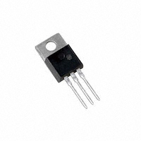
TO−220AB
CASE 221A−09
STYLE 1
1
2
3
THERMAL CHARACTERISTICS
Symbol
EMITTER 3
4
Stresses exceeding Maximum Ratings may damage the device. Maximum
Ratings are stress ratings only. Functional operation above the Recommended
Operating Conditions is not implied. Extended exposure to stresses above the
Recommended Operating Conditions may affect device reliability.
1. Pulse Width v 6.0 ms, Duty Cycle v 50%.
Characteristic
1
BASE
70
2.0
−55 to +150
COLLECTOR 2, 4
EMITTER 3
60
80
5.0
Operating and Storage Junction
Temperature Range
1
BASE
Unit
VEB
Collector Current − Continuous
NPN
PNP
D4xHyyG
AYWW
D4xHyy = Device Code
x = 4 or 5
yy = 8 or 11
A
= Assembly Location
Y
= Year
WW
= Work Week
G
= Pb−Free Package
ORDERING INFORMATION
Package
Shipping†
D44H8G
TO−220
(Pb−Free)
50 Units/Rail
D44H11G
TO−220
(Pb−Free)
50 Units/Rail
D45H8G
TO−220
(Pb−Free)
50 Units/Rail
D45H11G
TO−220
(Pb−Free)
50 Units/Rail
Device
†For information on tape and reel specifications,
including part orientation and tape sizes, please
refer to our Tape and Reel Packaging Specifications
Brochure, BRD8011/D.
Publication Order Number:
D44H/D
�D44H Series (NPN),
ELECTRICAL CHARACTERISTICS (TC = 25°C unless otherwise noted)
Symbol
Min
Typ
Max
Unit
VCEO(sus)
60
80
−
−
−
−
Vdc
Collector Cutoff Current (VCE = Rated VCEO, VBE = 0)
ICES
−
−
10
mA
Emitter Cutoff Current (VEB = 5.0 Vdc)
IEBO
−
−
10
mA
60
40
−
−
−
−
−
−
1.0
−
−
1.5
−
−
90
160
−
−
−
−
50
40
−
−
−
−
300
135
−
−
−
−
500
500
−
−
−
−
140
100
−
−
Characteristic
OFF CHARACTERISTICS
Collector−Emitter Sustaining Voltage
(IC = 30 mAdc, IB = 0 Adc)
D44H8, D45H8
D44H11, D45H11
ON CHARACTERISTICS
DC Current Gain
(VCE = 1.0 Vdc, IC = 2.0 Adc)
(VCE = 1.0 Vdc, IC = 4.0 Adc)
hFE
Collector−Emitter Saturation Voltage
(IC = 8.0 Adc, IB = 0.4 Adc)
VCE(sat)
Base−Emitter Saturation Voltage
(IC = 8.0 Adc, IB = 0.8 Adc)
VBE(sat)
−
Vdc
Vdc
DYNAMIC CHARACTERISTICS
Collector Capacitance
(VCB = 10 Vdc, ftest = 1.0 MHz)
Gain Bandwidth Product
(IC = 0.5 Adc, VCE = 10 Vdc, f = 20 MHz)
D44H Series
D45H Series
Ccb
pF
fT
D44H Series
D45H Series
MHz
SWITCHING TIMES
Delay and Rise Times
(IC = 5.0 Adc, IB1 = 0.5 Adc)
Storage Time
(IC = 5.0 Adc, IB1 = IB2 = 0.5 Adc)
Fall Time
(IC = 5.0 Adc, IB1 = 102 = 0.5 Adc)
D44H Series
D45H Series
td + tr
D44H Series
D45H Series
D44H Series
D45H Series
http://onsemi.com
2
ns
ts
ns
tf
ns
�D44H Series (NPN),
1000
1000
VCE = 1 V
25°C
hFE, DC CURRENT GAIN
hFE, DC CURRENT GAIN
VCE = 1 V
125°C
−40°C
100
10
0.01
0.1
1
125°C
25°C
100
10
10
−40°C
0.01
Figure 1. D44H11 DC Current Gain
Figure 2. D45H11 DC Current Gain
1000
hFE, DC CURRENT GAIN
25°C
−40°C
100
0.01
0.1
1
100
−40°C
0.01
0.1
1
10
IC, COLLECTOR CURRENT (AMPS)
Figure 3. D44H11 DC Current Gain
Figure 4. D45H11 DC Current Gain
0.6
0.30
−40°C
0.25
0.20
25°C
0.15
125°C
0.10
0.05
0.1
25°C
IC, COLLECTOR CURRENT (AMPS)
VCE(sat) @ IC/IB = 10
0.35
125°C
10
10
SATURATION VOLTAGE (VOLTS)
hFE, DC CURRENT GAIN
VCE = 5 V
125°C
0.40
SATURATION VOLTAGE (VOLTS)
10
IC, COLLECTOR CURRENT (AMPS)
VCE = 5 V
0
1
IC, COLLECTOR CURRENT (AMPS)
1000
10
0.1
1
VCE(sat) @ IC/IB = 10
0.5
0.4
0.3
25°C
125°C
0.2
0.1
0
10
−40°C
0.1
1
IC, COLLECTOR CURRENT (AMPS)
IC, COLLECTOR CURRENT (AMPS)
Figure 5. D44H11 ON−Voltage
Figure 6. D45H11 ON−Voltage
http://onsemi.com
3
10
�D44H Series (NPN),
1.4
−40°C
1.0
0.8
125°C
0.6
25°C
0.4
0.2
0
IC, COLLECTOR CURRENT (AMPS)
SATURATION VOLTAGE (VOLTS)
VBE(sat) @ IC/IB = 10
0.1
1
0.6
25°C
0.4
0.2
0.1
1
100 ms
10 ms
TC ≤ 70° C
dc
DUTY CYCLE ≤ 50%
1.0 ms
0.5
0.3
0.2
D44H/45H8
D44H/45H10,11
2.0 3.0 5.0 7.0 10
20 30
50 70 100
VCE, COLLECTOR−EMITTER VOLTAGE (VOLTS)
TA TC
3.0 60
2.0 40
TC
TA
1.0 20
0
0
0
20
r(t), TRANSIENT THERMAL
RESISTANCE (NORMALIZED)
Figure 9. Maximum Rated Forward Bias
Safe Operating Area
1.0
0.7
0.5
140
160
Figure 10. Power Derating
0.1
0.1
0.02
0.01
0.01 0.02
SINGLE PULSE
0.05
0.1
P(pk)
ZqJC(t) = r(t) RqJC
RqJC = 1.56°C/W MAX
D CURVES APPLY FOR POWER
PULSE TRAIN SHOWN
READ TIME AT t1
TJ(pk) - TC = P(pk) ZqJC(t)
0.05
0.03
0.01
60
80
100
120
T, TEMPERATURE (°C)
0.2
0.2
0.02
40
D = 0.5
0.3
0.07
0.05
10
Figure 8. D45H11 ON−Voltage
1.0 ms
1.0
125°C
Figure 7. D44H11 ON−Voltage
10
0.1
0.8
IC, COLLECTOR CURRENT (AMPS)
50
30
20
1.0
−40°C
1.0
IC, COLLECTOR CURRENT (AMPS)
100
5.0
3.0
2.0
VBE(sat) @ IC/IB = 10
1.2
0
10
PD, POWER DISSIPATION (WATTS)
SATURATION VOLTAGE (VOLTS)
1.2
0.2
0.5
1.0
2.0
5.0
10
t, TIME (ms)
Figure 11. Thermal Response
http://onsemi.com
4
20
t1
t2
DUTY CYCLE, D = t1/t2
50
100
200
500 1.0 k
�D44H Series (NPN),
PACKAGE DIMENSIONS
TO−220
CASE 221A−09
ISSUE AG
−T−
B
F
SEATING
PLANE
C
T
S
4
DIM
A
B
C
D
F
G
H
J
K
L
N
Q
R
S
T
U
V
Z
A
Q
U
1 2 3
H
K
Z
L
R
V
NOTES:
1. DIMENSIONING AND TOLERANCING PER ANSI
Y14.5M, 1982.
2. CONTROLLING DIMENSION: INCH.
3. DIMENSION Z DEFINES A ZONE WHERE ALL
BODY AND LEAD IRREGULARITIES ARE
ALLOWED.
J
G
D
N
INCHES
MIN
MAX
0.570
0.620
0.380
0.405
0.160
0.190
0.025
0.036
0.142
0.161
0.095
0.105
0.110
0.161
0.014
0.025
0.500
0.562
0.045
0.060
0.190
0.210
0.100
0.120
0.080
0.110
0.045
0.055
0.235
0.255
0.000
0.050
0.045
----0.080
MILLIMETERS
MIN
MAX
14.48
15.75
9.66
10.28
4.07
4.82
0.64
0.91
3.61
4.09
2.42
2.66
2.80
4.10
0.36
0.64
12.70
14.27
1.15
1.52
4.83
5.33
2.54
3.04
2.04
2.79
1.15
1.39
5.97
6.47
0.00
1.27
1.15
----2.04
ON Semiconductor and
are registered trademarks of Semiconductor Components Industries, LLC (SCILLC). SCILLC owns the rights to a number of patents, trademarks,
copyrights, trade secrets, and other intellectual property. A listing of SCILLC’s product/patent coverage may be accessed at www.onsemi.com/site/pdf/Patent−Marking.pdf. SCILLC
reserves the right to make changes without further notice to any products herein. SCILLC makes no warranty, representation or guarantee regarding the suitability of its products for any
particular purpose, nor does SCILLC assume any liability arising out of the application or use of any product or circuit, and specifically disclaims any and all liability, including without
limitation special, consequential or incidental damages. “Typical” parameters which may be provided in SCILLC data sheets and/or specifications can and do vary in different applications
and actual performance may vary over time. All operating parameters, including “Typicals” must be validated for each customer application by customer’s technical experts. SCILLC
does not convey any license under its patent rights nor the rights of others. SCILLC products are not designed, intended, or authorized for use as components in systems intended for
surgical implant into the body, or other applications intended to support or sustain life, or for any other application in which the failure of the SCILLC product could create a situation where
personal injury or death may occur. Should Buyer purchase or use SCILLC products for any such unintended or unauthorized application, Buyer shall indemnify and hold SCILLC and
its officers, employees, subsidiaries, affiliates, and distributors harmless against all claims, costs, damages, and expenses, and reasonable attorney fees arising out of, directly or indirectly,
any claim of personal injury or death associated with such unintended or unauthorized use, even if such claim alleges that SCILLC was negligent regarding the design or manufacture
of the part. SCILLC is an Equal Opportunity/Affirmative Action Employer. This literature is subject to all applicable copyright laws and is not for resale in any manner.
PUBLICATION ORDERING INFORMATION
LITERATURE FULFILLMENT:
Literature Distribution Center for ON Semiconductor
P.O. Box 5163, Denver, Colorado 80217 USA
Phone: 303−675−2175 or 800−344−3860 Toll Free USA/Canada
Fax: 303−675−2176 or 800−344−3867 Toll Free USA/Canada
Email: orderlit@onsemi.com
N. American Technical Support: 800−282−9855 Toll Free
USA/Canada
Europe, Middle East and Africa Technical Support:
Phone: 421 33 790 2910
Japan Customer Focus Center
Phone: 81−3−5817−1050
http://onsemi.com
5
ON Semiconductor Website: www.onsemi.com
Order Literature: http://www.onsemi.com/orderlit
For additional information, please contact your local
Sales Representative
D44H/D
�


 工商网监
湘ICP备2023018690号
工商网监
湘ICP备2023018690号
