ON Semiconductor
Is Now
To learn more about onsemi™, please visit our website at
www.onsemi.com
onsemi and and other names, marks, and brands are registered and/or common law trademarks of Semiconductor Components Industries, LLC dba “onsemi” or its affiliates and/or
subsidiaries in the United States and/or other countries. onsemi owns the rights to a number of patents, trademarks, copyrights, trade secrets, and other intellectual property. A listing of onsemi
product/patent coverage may be accessed at www.onsemi.com/site/pdf/Patent-Marking.pdf. onsemi reserves the right to make changes at any time to any products or information herein, without
notice. The information herein is provided “as-is” and onsemi makes no warranty, representation or guarantee regarding the accuracy of the information, product features, availability, functionality,
or suitability of its products for any particular purpose, nor does onsemi assume any liability arising out of the application or use of any product or circuit, and specifically disclaims any and all
liability, including without limitation special, consequential or incidental damages. Buyer is responsible for its products and applications using onsemi products, including compliance with all laws,
regulations and safety requirements or standards, regardless of any support or applications information provided by onsemi. “Typical” parameters which may be provided in onsemi data sheets and/
or specifications can and do vary in different applications and actual performance may vary over time. All operating parameters, including “Typicals” must be validated for each customer application
by customer’s technical experts. onsemi does not convey any license under any of its intellectual property rights nor the rights of others. onsemi products are not designed, intended, or authorized
for use as a critical component in life support systems or any FDA Class 3 medical devices or medical devices with a same or similar classification in a foreign jurisdiction or any devices intended for
implantation in the human body. Should Buyer purchase or use onsemi products for any such unintended or unauthorized application, Buyer shall indemnify and hold onsemi and its officers, employees,
subsidiaries, affiliates, and distributors harmless against all claims, costs, damages, and expenses, and reasonable attorney fees arising out of, directly or indirectly, any claim of personal injury or death
associated with such unintended or unauthorized use, even if such claim alleges that onsemi was negligent regarding the design or manufacture of the part. onsemi is an Equal Opportunity/Affirmative
Action Employer. This literature is subject to all applicable copyright laws and is not for resale in any manner. Other names and brands may be claimed as the property of others.
�FMBM5401 — PNP General-Purpose Amplifier
FMBM5401
PNP General-Purpose Amplifier
C2
Description
E1
C1
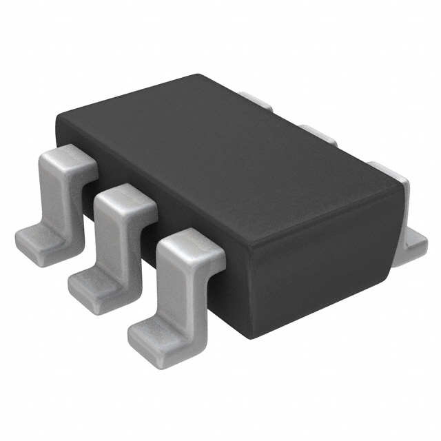
This device has matched dies in SuperSOT-6.
B2
E2
pin #1 B1
SuperSOTTM-6
Mark: .4S2
Ordering Information
Part Number
Marking
Package
Packing Method
FMBM5401
4S2
SSOT 6L
Tape and Reel
Absolute Maximum Ratings(1),(2)
Stresses exceeding the absolute maximum ratings may damage the device. The device may not function or be operable above the recommended operating conditions and stressing the parts to these levels is not recommended. In addition, extended exposure to stresses above the recommended operating conditions may affect device reliability. The
absolute maximum ratings are stress ratings only. Values are at TA = 25°C unless otherwise noted.
Symbol
Parameter
Value
Unit
VCEO
Collector-Emitter Voltage
-150
V
VCBO
Collector-Base Voltage
-160
V
VEBO
Emitter-Base Voltage
-5.0
V
-600
mA
-55 to +150
°C
IC
TJ, TSTG
Collector Current - Continuous
Operating and Storage Junction Temperature Range
Notes:
1. These ratings are based on a maximum junction temperature of 150°C.
2. These are steady-state limits. ON Semiconductor should be consulted on applications involving pulsed or lowduty-cycle operations.
Thermal Characteristics(3)
Values are at TA = 25°C unless otherwise noted.
Symbol
PD
RθJA
Parameter
Value
Unit
Total Power Dissipation
700
mW
Thermal Resistance, Junction-to-Ambient, Total
180
°C/W
Note:
3. Device mounted on a 1 in 2 pad of 2 oz copper.
© 2005 Semiconductor Components Industries, LLC.
October-2017,Rev. 2
Publication Order Number:
FMBM5401/D
�Values are at TA = 25°C unless otherwise noted.
Symbol
Parameter
Conditions
(4)
Min.
Max.
Unit
BVCEO
Collector-Emitter Breakdown Voltage
IC = -1.0 mA, IB = 0
-150
V
BVCBO
Collector-Base Breakdown Voltage
IC = -100 μA, IE = 0
-160
V
BVEBO
Emitter-Base Breakdown Voltage
IE = -10 μA, IC = 0
-5.0
V
ICBO
Collector Cut-Off Current
IEBO
Emitter Cut-Off Current
hFE1
DIVID1
hFE2
DIVID2
hFE3
DIVID3
DC Current Gain
(4)
VCB = -120 V, IE = 0
-50
nA
VCB = -120 V, IE = 0, TA = 100°C
-50
μA
VEB = -3.0 V, IC = 0
-50
nA
VCE = -5 V, IC = -1 mA
50
Variation Ratio of hFE1
Between Die 1 and Die 2
hFE1(Die1) / hFE1(Die2)
0.9
1.1
DC Current Gain(4)
VCE = -5 V, IC = -10 mA
60
240
Variation Ratio of hFE2
Between Die 1 and Die 2
hFE2(Die1) / hFE2(Die2)
0.95
1.05
DC Current Gain(4)
VCE = -5 V, IC = -50 mA
50
Variation Ratio of hFE3
Between Die 1 and Die 2
hFE3(Die1) / hFE3(Die2)
0.9
1.1
IC = -10 mA, IB = -1 mA
-0.2
IC = -50 mA, IB = -5 mA
-0.5
IC = -10 mA, IB = -1 mA
-1
IC = -50 mA, IB = -5 mA
-1
Base-Emitter On Voltage(4)
VCE = -5 V, IC = -10 mA
-1
V
Difference of VBE(on)
Between Die1 and Die 2
VBE(on)(Die1) - VBE(on)(Die2)
-8
8
mV
Current Gain Bandwidth Product
VCE = -10 V, IC = -10 mA,
f = 100 MHz
100
300
MHz
Cob
Output Capacitance
VCB = -10 V, IE = 0, f = 1 MHz
6.0
pF
NF
Noise Figure
VCE = -5.0 V, IC = -250 μA,
RS = 1.0 kΩ,
f = 10 Hz to 15.7 kHz
8.0
dB
VCE(sat) Collector-Emitter Saturation Voltage(4)
VBE(sat) Base-Emitter Saturation Voltage(4)
VBE(on)
DEL
fT
Note:
4. Pulse test: Pulse width ≤ 300 ms, duty cycle ≤ 2%
www.onsemi.com
2
V
V
FMBM5401 — PNP General-Purpose Amplifier
Electrical Characteristics
�β
β = 10
β
0.3
150
o
125 C
o
25 C
0.2
100
o
25 C
50
o
- 40 C
0
1E-4
o
125 C
0.1
1E-3
0.01
0.1
1
IC - COLLECTOR CURRENT (A)
Figure 1. Typical Pulsed Current Gain
vs. Collector Current
o
- 40 C
0.0
0.1
10
100
Figure 2. Collector-Emitter Saturation Voltage
vs. Collector Current
1.0
VBESAT - BASE-EMITTER VOLTAGE (V)
1.0
o
- 40 C
0.8
o
- 40 C
0.8
o
25 C
o
25 C
0.6
0.6
o
125 C
β
o
125 C
0.4
0.4
β
0.2
0.1
1
β = 10
10
100
VCE = 5V
0.2
0.1
1
10
100
IC - COLLECTOR CURRENT (mA)
IC - COLLECTOR CURRENT (mA)
Figure 4. Base-Emitter On Voltage
vs.Collector Current
100
BV CER - BREAKDOWN VOLTAGE (V)
Figure 3. Base-Emitter Saturation Voltage
vs. Collector Current
I CBO - COLLECTOR CURRENT (nA)
1
IC - COLLECTOR CURRENT (mA)
VBC(ON) - BASE-EMITTER ON VOLTAGE (V)
hFE - TYPICAL PULSED CURRENT GAIN
VCE = 5V
VCESAT - COLLECTOR-EMITTER VOLTAGE (V)
0.4
200
Between Emitter-Base
220
V CB = 10 0V
10
210
200
1
190
0.1
180
25
50
75
100
125
T A - AM BIENT TE MPE RATURE (°C)
Figure 5. Collector Cut-Off Current
vs. Ambient Temperature
150
170
0.1
1
10
RESISTANCEΩ(kΩ )
100
1000
Figure 6. Collector-Emitter Breakdown Voltage with
Resistance Between Emitter-Base
www.onsemi.com
3
FMBM5401 — PNP General-Purpose Amplifier
Typical Performance Characteristics
�80
CAPACITANCE (pF)
f = 1.0 MHz
60
40
C eb
20
C cb
0
0.1
1
10
100
V R - REVERSE BIAS VOLTAGE(V)
Figure 7. Input and Output Capacitance
vs. Reverse Voltage
www.onsemi.com
4
FMBM5401 — PNP General-Purpose Amplifier
Typical Performance Characteristics (Continued)
�FMBM5401 — PNP General-Purpose Amplifier
Physical Dimensions
Figure 8. 6-LEAD, SUPERSOT6, JEDEC MO-193, 1.6MM WIDE
www.onsemi.com
5
�ON Semiconductor and
are trademarks of Semiconductor Components Industries, LLC dba ON Semiconductor or its subsidiaries in the United States and/or other countries.
ON Semiconductor owns the rights to a number of patents, trademarks, copyrights, trade secrets, and other intellectual property. A listing of ON Semiconductor’s product/patent
coverage may be accessed at www.onsemi.com/site/pdf/Patent−Marking.pdf. ON Semiconductor reserves the right to make changes without further notice to any products herein.
ON Semiconductor makes no warranty, representation or guarantee regarding the suitability of its products for any particular purpose, nor does ON Semiconductor assume any liability
arising out of the application or use of any product or circuit, and specifically disclaims any and all liability, including without limitation special, consequential or incidental damages.
Buyer is responsible for its products and applications using ON Semiconductor products, including compliance with all laws, regulations and safety requirements or standards,
regardless of any support or applications information provided by ON Semiconductor. “Typical” parameters which may be provided in ON Semiconductor data sheets and/or
specifications can and do vary in different applications and actual performance may vary over time. All operating parameters, including “Typicals” must be validated for each customer
application by customer’s technical experts. ON Semiconductor does not convey any license under its patent rights nor the rights of others. ON Semiconductor products are not
designed, intended, or authorized for use as a critical component in life support systems or any FDA Class 3 medical devices or medical devices with a same or similar classification
in a foreign jurisdiction or any devices intended for implantation in the human body. Should Buyer purchase or use ON Semiconductor products for any such unintended or unauthorized
application, Buyer shall indemnify and hold ON Semiconductor and its officers, employees, subsidiaries, affiliates, and distributors harmless against all claims, costs, damages, and
expenses, and reasonable attorney fees arising out of, directly or indirectly, any claim of personal injury or death associated with such unintended or unauthorized use, even if such
claim alleges that ON Semiconductor was negligent regarding the design or manufacture of the part. ON Semiconductor is an Equal Opportunity/Affirmative Action Employer. This
literature is subject to all applicable copyright laws and is not for resale in any manner.
PUBLICATION ORDERING INFORMATION
LITERATURE FULFILLMENT:
Literature Distribution Center for ON Semiconductor
19521 E. 32nd Pkwy, Aurora, Colorado 80011 USA
Phone: 303−675−2175 or 800−344−3860 Toll Free USA/Canada
Fax: 303−675−2176 or 800−344−3867 Toll Free USA/Canada
Email: orderlit@onsemi.com
❖
© Semiconductor Components Industries, LLC
N. American Technical Support: 800−282−9855 Toll Free
USA/Canada
Europe, Middle East and Africa Technical Support:
Phone: 421 33 790 2910
Japan Customer Focus Center
Phone: 81−3−5817−1050
ON Semiconductor Website: www.onsemi.com
Order Literature: http://www.onsemi.com/orderlit
For additional information, please contact your local
Sales Representative
www.onsemi.com
�


 工商网监
湘ICP备2023018690号
工商网监
湘ICP备2023018690号
