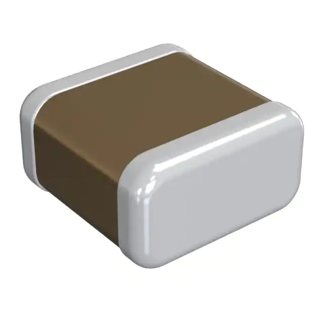
CHIP MONOLITHIC CERAMIC CAPACITOR
GRM0335C1HR30WD01_ (0201, C0G, 0.3pF, 50Vdc)
_: packaging code
Reference Sheet
1.Scope
This product specification is applied to Chip Monolithic Ceramic Capacitor used for General Electronic equipment.
2.MURATA Part NO. System
(Ex.)
GRM
03
(1)L/W
Dimensions
3
5C
1H
R30
W
D01
(2)T
(3)Temperature (4)DC Rated (5)Nominal (6)Capacitance (7)Murata’s (8)Packaging
Code
Dimensions Characteristics
Voltage
Capacitance Tolerance
Control Code
3. Type & Dimensions
L
W
T
e
g
e
(Unit:mm)
g
(1)-1 L
(1)-2 W
(2) T
e
0.6±0.03
0.3±0.03
0.3±0.03
0.1 to 0.2
0.2 min.
4.Rated value
(3) Temperature Characteristics
(Public STD Code):F(EIA)
Temp. coeff
Temp. Range
or Cap. Change
(Ref.Temp.)
0±30 ppm/°C
25 to 125 °C
(25 °C)
(4)
DC Rated
Voltage
50 Vdc
(6)
(5) Nominal
Capacitance
Capacitance
Tolerance
0.3 pF
±0.05 pF
Specifications and Test
Methods
(Operationg
Temp. Range)
-55 to 125 °C
5.Package
mark
D
J
D
(8) Packaging
f180mm Reel
PAPER
f330mm Reel
PAPER
Packaging Unit
15000 pcs./Reel
50000 pcs./Reel
B
Bulk Bag
1000 pcs./Bag
C
Bulk Case
50000 pcs./Case
Product specifications in this catalog are as of Aug.3,2011,and are subject to change or obsolescence without notice.
Please consult the approval sheet before ordering.
Please read rating and !Cautions first.
GRM0335C1HR30WD01-01
1
�SPECIFICATIONS AND
TEST
METHODS
Specification
No.
Item
Temperature
Compensating Type
1
Operating Temperature
Range
-55C
2
Rated Voltage
See the previous pages
3
4
5
Appearance
Dimension
Dielectric
Strength
No defects or abnormalities
Within the specified dimensions
No defects or abnormalities
6
Insulation Resistance
More than 10,000M or 500∙F
(whichever is smaller)
7
8
Capacitance
Q/
Dissipation Factor
(D.F.)
Within the specified tolerance
[R6,R7,C8,L8]
30pF and over :
W.V.:100V
: 0.025max.(C < 0. 068F)
Q ≧ 1000
: 0.05max.(C ≧ 0.068F)
W.V.:25/50V :0.025max.
30pF and below :
W.V.:16/10V :0.035max.
Q ≧ 400+20C
W.V.:6.3V/4V :0.05max. (C < 3.3F)
:0.1max.(C ≧ 3.3F)
C:Nominal
[R9]W.V.:50V: 0.05max.
Capacitance (pF) [E4] W.V.:25Vmin :0.025max.
[F5] W.V.:25Vmin.
:0.05max. (C 0.1F) :0.09max. (C ≧ 0.1F)
W.V.:16/10V:0.125max. W.V.:6.3V:0.15max.
9
to +125C
Test
High Dielectric Type
Capacitance Capacitance Within the specified
Temperature Change
tolerance.
Character-ist
(Table A -1)
ics
R6 : -55C to + 85C
R7 : -55C to +125C
C8 : -55C to + 105C E4 : 10C to + 85C
F5 : -30C to + 85C
L8/R9 : -55C to +150C
Char.
Coefficent
Reference
Temp.
Cap. Change
R6
-55C to +85C
Within ±15%
R7
C8
-55C to +125C
-55C to +105C
Within ±15%
Within ±22%
L8
Temperature
Temp. Range
-55C to +125C
25C
+125C to+150C
Within ±15%
Within+15/-40%
R9
-55C to+150C
Within ±15%
E4
+10C to +85C
Within+22/-56%
F5
-30C to +85C
Within+22/-82%
Within the specified tolerance.
(Table A -1)
Capacitance Within ±0.2% or ±0.05 pF
Drift
(Whichever is larger.)
Not apply to 1X/25V
10 Adhesive Strength of
Termination
a
c
b
Reference Temperature : 25C
The rated voltage is defined as the maximum voltage which may be
applied continuously to the capacitor. When AC voltage is
superimposed on DC voltage, VP-P or VO-P, whichever is larger,
should be maintained within the rated voltage range.
Visual inspection.
Using calipers or Microscope. (GRM02 size is based on Microscope)
No failure should be observed when 300% of the rated voltage (C
to 7U and 1X) or 250% of the rated voltage (R6, R7,C8,E4 and F5) is
applied between the terminations for 1 to 5 seconds, provided the
charge/ discharge current is less than 50mA.
The insulation resistance should be measured with a DC voltage not
exceeding the rated voltage at 25C and 75%RH max. and within 2
minutes of charging.
The capacitance/Q/D.F. should be measured at 25C at the
frequency and voltage shown in the table.
Char.
C
C
to 7U,1X
to 7U,1X
(1000pF and (more than 1000pF)
below)
R6,R7,C8,F5
(C ≦ 10F)
R6,R7,F5
(C>10F)
E4
Item
Frequency
Voltage
1±0.1MHz
1±0.1kHz
0.5 to 5Vrms
1±0.2Vrms
120±24Hz
1±0.1kHz
0.5±0.1Vrms 0.5±0.05Vrms
The capacitance change should be measured after 5 min. at
each specified temperature stage.
(1)Temperature Compensating Type
The temperature coefficient is determind using the capacitance
measured in step 3 as a reference. When cycling the temperature
sequentially from step1 through 5 (C+25C to +125C , other
temp. coeffs.:+25C to +85C ) the capacitance should be within
the specified tolerance for the temperature coefficient and
capacitance change as Table A-1. The capacitance drift is
caluculated by dividing the differences betweeen the maximum and
minimum measured values in the step 1,3 and 5 by the cap value in
step 3.
Step
Temperature(C )
1
2
25±2
-55±3(forC to 7U/1X/R6/R7/C8/L8/R9)
-30±3(for F5), 10±3(for E4)
3
4
25±2
150±3(for R9),125±3(for C/R7),
105±3(for C8),85±3(for other TC)
5
25±2
(2) High Dielectric Constant Type
The ranges of capacitance change compared with the 25C value
over the temperature ranges shown in the table should be within
the specified ranges.
Initial measurement for high dielectric constant type.
Perform a heat treatment at 150+0/-10C for one hour
and then set for 24±2 hours at room temperature.
Perform the initial measurement.
Solder the capacitor to the test jig (glass epoxy board) shown in Fig.1
using a eutectic solder. Then apply *10N force in parallel with the test
jig for 10±1sec.
The soldering should be done either with an iron or using the reflow
method and should be conducted with care so that the soldering is
uniform and free of defects such as heat shock
*5N (GR15, GRM18)
2N (GR03),1N(GR02)
No removal of the terminations or other defect should occur.
Solder resist
Fig.1
Method
Baked electrode or
copper foil
Type
a
b
c
GR02
0.2
0.56
0.23
GR03
0.3
0.9
0.3
GR15
0.4
1.5
0.5
GRM18
1.0
3.0
1.2
GRM21
1.2
4.0
1.65
GRM31
2.2
5.0
2.0
GRM32
2.2
5.0
2.9
GRM43
3.5
7.0
3.7
GRM55
4.5
8.0
5.6
(in:mm)
JEMCGS-0015Q
2
�SPECIFICATIONS AND
TEST
METHODS
Specification
No.
Item
Temperature
Compensating Type
Test
High Dielectric Type
11 Vibration Appearance No defects or abnormalities
Resistance Capacitance Within the specified tolerance
Q/D.F.
30pF and over :
[R6,R7,C8,L8]
Q ≧ 1000
W.V.:100V
: 0.025max. (C < 0. 068F)
: 0.05max.(C ≧ 0.068F)
30pF and below:
W.V.:25/50V :0.025max.
Q ≧ 400+20C
W.V.:16/10V :0.035max.
W.V.:6.3V/4V :0.05max. (C < 3.3F)
C:Nominal
:0.1max.(C ≧ 3.3F)
Capacitance (pF)
[R9]W.V.:50V: 0.05max.
[E4] W.V.:25Vmin. :0.025max
[F5] W.V.:25Vmin.
:0.05max. (C 0.1F) :0.09max.(C ≧ 0.1F)
W.V.:16/10V:0.125max. W.V.:6.3V:0.15max.
12 Deflection Appearance No defects or abnormalities.
Capacitance Within ± 5% or ± Within ±10%
Change
0.5pF
(Whichever is larger)
Method
Solder the capacitor on the test jig (glass epoxy board) in the
same manner and under the same conditions as(10). The
capacitor should be subjected to a simple harmonic motion
having a total amplitude of 1.5mm, the frequency being varied
uniformly between the approximate limits of 10 and 55Hz. The
frequency range, from 10 to 55Hz and return to 10Hz, should be
traversed in approximately 1 minute. This motion should be
applied for a period of 2 hours in each 3 mutually perpendicular
directions(total of 6 hours).
Solder the capacitor on the test jig (glass epoxy board) shown in
Fig.2 using a eutectic solder. Then apply a force in the direction
shown in Fig 3 for 5±1sec. The soldering should be done by the
reflow method and should be conducted with care so that the
soldering is uniform and free of defects such as heat shock.
f4.5
c
40
b
a
100
R230
20 50
Pressunzing
speed:1.0mm/sec.
Pressunze
(GR02/03,GR15:0.8mm)
Type
GR02
GR03
GR15
GRM18
GRM21
GRM31
GRM32
GRM43
GRM55
Flexure: ≦1
Capacitance meter
45
45
Fig.3
13 Solderability of
Termination
75% of the terminations is to be soldered evenly and continuously
14 Resistance to
Soldering Heat
The measured and observed characteristics should satisfy the specifications in
the following table
Appearance No defects or abnormalities
Capacitance Within ±2.5% or ±0.25pF
Change
(Whichever is larger)
t : 1.6mm
Fig.2
R6,R7,C8,L8,R9:Within ±7.5%
E4,F5:Within ±20%
a
0.2
0.3
0.4
1.0
1.2
2.2
2.2
3.5
4.5
b
0.56
0.9
1.5
3.0
4.0
5.0
5.0
7.0
8.0
c
0.23
0.3
0.5
1.2
1.65
2.0
2.9
3.7
5.6
(in:mm)
Immerse the capacitor in a solution of ethanol(JIS-K-8101) and
rosin (JIS-K-5902) (25% rosin in weight propotion). Preheat at
80 to 120C for 10 to 30 seconds. After preheating , immerse
in an eutectic solder solution for 2±0.5 seconds at 230±5C or
Sn-3.0Ag-0.5Cu solder solution for 2±0.5 seconds at 245±
5C.
Preheat the capacitor at *120 to 150C for 1 minute. Immerse
the capacitor in an eutectic solder solution* or Sn-3.0Ag-0.5Cu
solder solution at 270±5C for 10±0.5 seconds. Set at room
temperature for 24±2 hours, then measure.
*Not apply to GRM02
∙ Initial measurement for high dielectric constant type
Perform a heat treatment at 150+0/-10C for one hour and
then set at room temperature for 24±2 hours.
Perform the initial measurement.
*Preheating for GRM32/43/55
Q/D.F.
I.R.
Dielectric
Strength
JEMCGS-0015Q
30pF and over :
Q ≧ 1000
[R6,R7,C8,L8]
W.V.:100V
: 0.025max.(C < 0. 068F)
: 0.05max. (C ≧ 0.068F)
30pF and below:
W.V.:25/50V :0.025max.
Q ≧ 400+20C
W.V.:16/10V :0.035max.
W.V.:6.3V/4V :0.05max.(C < 3.3F)
C:Nominal
:0.1max.(C ≧ 3.3F)
Capacitance (pF)
[R9]W.V.:50V: 0.05max.
[E4] W.V.:25Vmin :0.025max
[F5] W.V.:25Vmin
:0.05max. (C 0.1F) :0.09max. (C ≧ 0.1F)
W.V.:16/10V:0.125max. W.V.:6.3V:0.15max.
More than 10,000Mor 500F(Whichever is smaller)
No defects
3
Step
Temperature
Time
1
100C
to 120C
1 min.
2
170C
to 200C
1 min.
�SPECIFICATIONS AND
TEST
METHODS
Specification
No.
Item
Temperature
Compensating Type
15 Temperature Cycle
The measured and observed characteristics should satisfy the specifications in
the following table
Appearance No defects or abnormalities
Capacitance Within ±2.5% or ±0.25pF
Change
(Whichever is larger)
Q/D.F.
I.R.
Dielectric
Strength
R6,R7,C8,L8,R9:Within ±7.5%
E4,F5:Within ±20%
30pF and over :
Q ≧ 1000
[R6,R7,C8,L8]
W.V.:100V
: 0.025max. (C < 0. 068F)
: 0.05max.(C ≧ 0.068F)
30pF and below:
W.V.:25/50V :0.025max.
Q ≧ 400+20C
W.V.:16/10V :0.035max.
W.V.:6.3V/4V :0.05max. (C < 3.3F)
C:Nominal
:0.1max. (C ≧ 3.3F)
Capacitance (pF)
[R9]W.V.:50V: 0.05max.
[E4] W.V.:25Vmin. :0.025max
[F5] W.V.:25Vmin.
:0.05max. (C 0.1F) :0.09max.(C ≧ 0.1F)
W.V.:16/10V:0.125max. W.V.:6.3V:0.15max.
More than 10,000Mor 500F (Whichever is smaller)
Capacitance Within ±5% or ±0.5pF
Change
(Whichever is larger)
I.R.
Dielectric
Strength
17 Humidity Load
R6,R7,C8,L8,R9:Within ±12.5%
E4,F5:Within ±30%
Dielectric
Strength
JEMCGS-0015Q
Step
Temp.(C)
Time
(min.)
1
Min.
Operating
Temp. +0/-3
30±3
2
Room
Temp.
2 to 3
3
Max.
Operating
Temp. +3/-0
30±3
4
Room
Temp.
2 to 3
∙ Initial measurement for high dielectric constant type
Perform a heat treatment at 150+0/-10C for one hour and
then set at room temperature for 24±2 hours. Perform the initial
measurement
Set the capacitor at 40±2C and in 90 to 95% humiduty for
500±12 hours.
Remove and set for 24±2 hours at room temperature, then
measure.
[R6,R7,C8,L8]
W.V.:100V
: 0.05max. (C < 0.068F)
: 0.075max. (C ≧ 0.068F)
30pF and below:
W.V.:25/50V :0.05max.
Q ≧ 275 + 5 C
2
W.V.:16/10V :0.05max.
W.V.:6.3V/4V:0.075max. (C < 3.3F)
:0.125max. (C ≧ 3.3F)
10pF and below:
[R9]W.V.:50V: 0.075max.
Q ≧ 200+10C
[E4] W.V.:25Vmin.:0.05max.
C:Nominal
Capacitance(pF)
[F5] W.V.:25Vmin.
:0.075max. (C0.1F) :0.125max. (C≧0.1F)
W.V.:16/10V:0.15max. W.V.:6.3V:0.2max.
More than 1,000Mor 50F(Whichever is smaller)
No defects
The measured and observed characteristics should satisfy the specifications in
the following table
R6,R7,C8,L8,R9:Within ±12.5%
E4:Within ±30%
F5:Within ±30% (W.V.>10V)
F5:Within +30/-40% (W.V. ≦10V)
30pF and over : Q ≧ 200
[R6,R7,C8,L8]
W.V.:100V
: 0.05max. (C < 0.068F)
: 0.075max. (C ≧ 0.068F)
W.V.:25/50V :0.05max.
W.V.:16/10V :0.05max.
C:Nominal
W.V.:6.3V/4V:0.075max. (C < 3.3F)
Capacitance(pF)
:0.125max. (C ≧ 3.3F)
[R9]W.V.:50V: 0.075max.
[E4] W.V.:25Vmin.:0.05max.
[F5] W.V.:25Vmin.
:0.075max. (C0.1F) :0.125max. (C≧0.1F)
W.V.:16/10V:0.15max. W.V.:6.3V:0.2max.
More than 500M or 25∙F(Whichever is smaller)
30pF and below:
Q≧100 + 10 C
3
I.R.
Fix the capacitor to the supporting jig in the same manner and
under the same conditions as (10). Perform the five cycles
according to the four heat treatments shown in the following
table. Set for 24±2 hours at room temperature, then measure
30pF and over : Q ≧ 350
10pF and over,
Appearance No defects or abnormalities
Capacitance Within ±7.5% or ±0.75pF
Change
(Whichever is larger)
Q/D.F.
Method
No defects
16 Humidity
The measured and observed characteristics should satisfy the specifications in
Steady State
the following table
Appearance No defects or abnormalities
Q/D.F.
Test
High Dielectric Type
No defects
4
Apply the rated voltage at 40±2C and 90 to 95% humidity for
500±12 hours.
Remove and set for 24±2 hours at room temprature, then
measure.
The charge/discharge current is less than 50mA.
∙Initial measurement for F5/16Vmax.
Apply the rated DC voltage for 1 hour at 40±2C .
Remove and set for 24±2 hours at room temperature.
Perform initial measurement.
�SPECIFICATIONS AND
TEST
METHODS
Specification
No.
Item
Temperature
Compensating Type
Test
High Dielectric Type
Method
18 High Temperature
Load
The measured and observed characteristics should satisfy the specifications Apply 200% of the rated voltage at the maximun operating
in the following table
temperature ±3C for 1000±12 hours . Set for 24±2 hours at
room temperature, then measure.
Appearance No defects or abnormalities
The charge/discharge current is less than 50mA.
Capacitance Within ±3% or ±0.3pF
R6,R7,C8,L8,R9:Within ±12.5%
Change
(Whichever is larger)
E4:Within ±30%
∙Initial measurement for high dielectric constant type.
F5:Within±30% (Cap


 工商网监
湘ICP备2023018690号
工商网监
湘ICP备2023018690号
