Preliminary Specification Number: SP-HNZY-N
Bluetooth Low Energy Module Data Sheet
Dialog Semiconductor Chipset
for Bluetooth 4.2
Tentative P/N : LBCA2HNZYZ-TEMP
Preliminary
< Specification may be changed by Murata without notice >
Murata Manufacturing Co., Ltd.
�Preliminary Specification Number: SP-HNZY-N
1/22
Revision History
Revision
Code
Date
Oct.24.2013
A
Feb.13.2014
B
Mar.20.2014
Description
First issue
4. Dimensions and Terminal Configurations
Added Dimensions of m6 and m7
5. Revised Absolute Maximum Ratings
6. Revised Operating Condition
10. Revised RF Characteristics
12. Recommended Land Pattern
Corrected to Top view
11. packing Information
Added the figure of Tape and Reel
1. Revised Scope
Added the weight
C
Apr.23.2014
D
Apr.29.2014
E
Jun.04.2014
F
Jul.02.2014
G
Nov.6.2014
5.Revised Absolute Maximum Ratings
8.Revised Sleep Clock for 32kHz Crystal
10.Revised RF Characteristics
13.Revised Application Circuit
11.Revised Packing Information
5.Revised Absolute Maximum Ratings
6. Operating Conditions
10.Revised RF Characteristics
4.Revised Dimensions and Terminal Configurations
10.Revised RF Characteristics
13.Revised Application Circuit
1.Scope
2.Part Number
3.RoHS Compliance
5.Dimensions and Terminal Configurations
6. Absolute Maximum Ratings
7.Operating Conditions
9.Sleep Clock: Recommended Operating Conditions
14.Application Circuit
15,Other Attentions
H
I
J
K
Feb.12.2014
Feb.23.2015
Feb.27.2015
Aug.10.2018
L
Oct.24.2018
M
Jun.19.2020
N
Jun.22.2020
16.Wireless / BT Certification Numbers
14. Application Circuit
16. Wireless / BT Certification Numbers
14. Application Circuit
16. Wireless / BT Certification Numbers
Front Page BT Spec Version
16. Wireless / BT Certification Numbers
16. Wireless / BT Certification Numbers
Modified Soldering Conditions.
12. Packing Information
Modified 1 pin mark information.
Preliminary
< Specification may be changed by Murata without notice >
Murata Manufacturing Co., Ltd.
�Preliminary Specification Number: SP-HNZY-N
2/22
TABLE OF CONTENTS
TABLE OF CONTENTS ............................................................................................................................. 2
1. Scope ................................................................................................................................................. 3
2. Part Number....................................................................................................................................... 3
3. RoHS Compliance ............................................................................................................................. 3
4. Block Diagram ................................................................................................................................... 3
5. Dimensions and Terminal Configurations ..................................................................................... 4
6. Absolute Maximum Ratings............................................................................................................. 7
7. Recommend Operating Condition .................................................................................................. 7
8. DC Characteristics ............................................................................................................................ 8
9. Sleep Clock: Recommended Operating Conditions ..................................................................... 8
10. Power Sequence ............................................................................................................................... 9
11. RF Characteristics .......................................................................................................................... 10
12. Packing Information ....................................................................................................................... 11
13. Recommended Land Pattern ......................................................................................................... 14
14. Application Circuit .......................................................................................................................... 15
15. Other Attentions .............................................................................................................................. 18
16. Wireless / BT Certification Numbers ............................................................................................ 18
17. NOTICE............................................................................................................................................. 19
18. PRECONDITION TO USE OUR PRODUCTS ................................................................................. 22
Please be aware that an important notice concerning availability, standard warranty, and use in critical
applications of Murata products and disclaimers thereto appears at the end of this specification sheet.
Preliminary
< Specification may be changed by Murata without notice >
Murata Manufacturing Co., Ltd.
�Preliminary Specification Number: SP-HNZY-N
3/22
1. Scope
This specification is applied to the Bluetooth low energy module.
- Interface
- IC
- Reference Clock
- Weight
- MSL
: GPIO(supporting UART / SPI / I2C)
: DA14580-01 (Dialog Semiconductor)
: Internal Crystal.
: 0.107g
:3
2. Part Number
Sample
Design Kit
Daughter Board
LBCA2HNZYZ-TEMP
LBCA2HNZYZ-TEMP-DK
LBCA2HNZYZ-TEMP-D-MU
3. RoHS Compliance
This component can meet with RoHS compliance.
4. Block Diagram
External X’tal / TCXO
(32.768kHz)
X’tal (16MHz)
Antenna
BLE IC
LC Network
for DCDC
UART /SPI/I2C
GPIO/ADC
Quadrature
Decoder
Power
Source
Preliminary
< Specification may be changed by Murata without notice >
Murata Manufacturing Co., Ltd.
�Preliminary Specification Number: SP-HNZY-N
4/22
5. Dimensions and Terminal Configurations
Pin 1 Marking
(unit: mm)
Dimension
Mark
Dimensions
Mark
Dimensions
Mark
Dimensions
Mark
Dimensions
L
7.4±0.25
W
7.0±0.25
T
1.0 Max
a1
0.3±0.1
a2
0.3±0.1
b1
0.3±0.2
b2
0.425±0.2
b3
0.425±0.2
c1
0.6±0.1
c2
0.6±0.1
e1
0.35±0.1
e2
0.35±0.1
e3
0.35±0.1
e4
0.5±0.1
e5
0.5±0.1
e6
0.4±0.1
e7
0.5±0.1
e8
0.5±0.1
m1
0.3±0.1
m2
0.6±0.1
m3
0.3±0.1
m4
0.3±0.1
m5
0.6±0.1
m6
3.3±0.2
m7
0.3±0.2
Preliminary
< Specification may be changed by Murata without notice >
Murata Manufacturing Co., Ltd.
�Preliminary Specification Number: SP-HNZY-N
5/22
Terminal Configurations
36
13
37
14
15
16
17
18
19
20
12
22
11
31
32
33
34
10
30
29
28
27
35
25
7
6
1
Terminal
Name
P0_5
Connection to
IC Terminal
P0_5
2
P0_7
P0_7
3
4
P0_6
SWCLK
P0_6
SWCLK
5
SWDIO
SWDIO
6
7
8
9
10
GND
VBAT
GND
XTAL32KP
XTAL32KM
GND
VBAT
GND
XTAL32KP
XTAL32KM
11
P0_3
P0_3
12
P0_2
P0_2
13
14
15
16
17
18
ANTout
ANTin
GND
GND
GND
GND
GND
GND
GND
GND
No.
23
24
9
8
21
5
4
3
2
1
26
Description
INPUT/OUTPUT with selectable pull up/down resistor.
Pull-down enabled during and after reset. General
purpose I/O port bit or alternate function nodes. Contain
state retention mechanism during power down.
INPUT JTAG clock signal
INPUT/OUTPUT. JTAG Data input/output. Bidirectional
data and control communication
Ground
INPUT Battery connection.
Ground
INPUT. Crystal input for the 32.768 kHz XTAL
OUTPUT. Crystal output for the 32.768 kHz XTAL
INPUT/OUTPUT with selectable pull up/down resistor.
Pull-down enabled during and after reset. General
purpose I/O port bit or alternate function nodes. Contain
state retention mechanism during power down.
RF input/output. Refer to reference schematic
Ground
Preliminary
< Specification may be changed by Murata without notice >
Murata Manufacturing Co., Ltd.
�Preliminary Specification Number: SP-HNZY-N
6/22
19
Terminal
Name
NC
Connection to
IC Terminal
-
20
GND
GND
21
GND
GND
22
P0_1
P0_1
23
P0_0
P0_0
24
P0_4
P0_4
25
RST
RST
26
GND
GND
27
GND
GND
28
GND
GND
29
GND
GND
No.
30
P1_1
P1_1
31
VPP
VPP
32
GND
GND
33
GND
GND
34
GND
GND
Description
No connection
Ground
INPUT/OUTPUT with selectable pull up/down resistor.
Pull-down enabled during and after reset. General
purpose I/O port bit or alternate function nodes. Contain
state retention mechanism during power down.
INPUT. Reset signal (Active High, Internally Pulled
Down). It can be open or connected to GND if not used.
Ground
INPUT/OUTPUT with selectable pull up/down resistor.
Pull-down enabled during and after reset. General
purpose I/O port bit or alternate function nodes. Contain
state retention mechanism during power down.
INPUT. This pin is used while OTP programming.
Should be left open when not programming.
Ground
35
P1_0
36
NC
INPUT/OUTPUT with selectable pull up/down resistor.
Pull-down enabled during and after reset. General
purpose I/O port bit or alternate function nodes. Contain
state retention mechanism during power down.
No Connection
37
NC
No Connection
P1_0
Marking Information
Preliminary
< Specification may be changed by Murata without notice >
Murata Manufacturing Co., Ltd.
�Preliminary Specification Number: SP-HNZY-N
7/22
6. Absolute Maximum Ratings
Item
Storage Temperature
VBAT supply voltage
Min
-40
-0.1
Max
85
3.6
Unit
degC
V
VPP supply voltage
-0.1
6.8
V
Remarks
Supply only during
OTP programming
Input voltage for
-0.2
Min(1.2,VBAT+0.2)
V
XTAL32KM
Input voltage for
-0.2
Min(1.5,VBAT+0.2)
V
XTAL32KP
Input voltage for
-0.1
Min(3.6,VBAT+0.2)
V
all other pins
Stresses in excess of the absolute ratings may cause permanent damage. Functional operation is
not implied under these conditions. Exposure to absolute ratings for extended periods of time may
adversely affect reliability. No damage assuming only one parameter is set at limit at a time with all
other parameters are set within operating condition.
7. Recommend Operating Condition
Item
Operating Temperature*1
VBAT supply voltage
VBAT supply voltage
for cold boot
Min
-40
2.35
VPP supply voltage
6.6
Typ
2.5
6.7
Max
85
3.3
Unit
degC
V
3.3
V
6.8
V
Remarks
Supply only during
OTP programming.
Input voltage for
0
Min(3.3,VBAT+0.2)
V
all other pins
RF Load Impedance
50
Ω
Output current for
4.8
mA
Each I/O pin
*1: Please keep derating / margin as much as possible at extreme temperature.
Preliminary
< Specification may be changed by Murata without notice >
Murata Manufacturing Co., Ltd.
�Preliminary Specification Number: SP-HNZY-N
8/22
8. DC Characteristics
Parameters
VIH
VIL
VOH
VOL
IIH(PD)
IIL(PU)
Description
HIGH level input voltage
LOW level input voltage
HIGH level output voltage
LOW level output voltage
HIGH level input current with
internal pull down enabled
LOW level input current with
internal pull up enabled
Conditions
Active mode
Active mode
Active mode
Active mode
Vin = VBAT
= 2.5V
Vin = GND
= 0V
Min
0.84
Typ
Max
0.47
Unit
V
V
V
V
50
150
uA
-150
-50
uA
Max
Unit
kHz
kohm
pF
pF
ppm
uW
0.36
1.88
9. Sleep Clock: Recommended Operating Conditions
For 32kHz Crystal
Parameters
fXTAL
ESR
CL
C0
dfXTAL
DLmax
Description
Crystal frequency
Equivalent Series Resistance
Load Capacitance
Shunt Capacitance
Crystal frequency tolerance
Maximum drive level
Conditions
Min
Typ
32.768
6
7
1
-250
0.1
100
9
2
250
For 32kHz Crystal Oscillator
Parameters
fXO
AXO
dfXO
Description
Oscillator frequency
Amplitude
Frequency tolerance
Conditions
Min
Typ
32.768
100
-250
Preliminary
< Specification may be changed by Murata without notice >
Murata Manufacturing Co., Ltd.
Max
1500
250
Unit
kHz
mVpp
ppm
�Preliminary Specification Number: SP-HNZY-N
9/22
10. Power Sequence
Power Up / Down Sequence
Power Up
Power Down
Td
H
VBAT
V1
L
Ta
Tb
H
GPIO
L
Reset and Power Cycle Sequence
Symbol
Description
Typ
Unit
Ta > 500
us
Ta
Time between VCC valid
and GPIO enabled
Tb
Time between GPIO invalid
and VCC invalid
Tb > 0
us
Tc
Length of RST pulse
Tc > 10
us
Td
Required VBAT ramp-up time
Td < 50
ms
V1
Threshold voltage of VBAT rise up
V1 > 2.35
V
Preliminary
< Specification may be changed by Murata without notice >
Murata Manufacturing Co., Ltd.
�Preliminary Specification Number: SP-HNZY-N
10/22
11. RF Characteristics
Normal Condition: VBAT=3.0V, +25deg.C, (otherwise notified)
Item / Conditions
Center frequency
Channel Spacing
Number of RF Channels
Output power (Measured at ANT pin)
Modulation characteristics
1) Δf1avg
2) Δf2max (at 99.9%)
3) Δf2avg / Δf1avg
Carrier frequency offset and drift
1) Frequency offset: | fn – fTX |
2) Frequency drift: | f0 – fn |
3) Drift rate #0: | f1 – f0 |
4) Drift rate #n: | fn – fn-5 |
Receiver sensitivity (Ideal transmitter PER
Murata Manufacturing Co., Ltd.
�Preliminary Specification Number: SP-HNZY-N
12/22
3.
Taping Diagrams
[1] Feeding Hole : As specified in (1)
[2] Hole for chip : As specified in (1)
[3] Cover tape
: 62μm in thickness
[4] Base tape
: As specified in (1)
[3]
[1]
[2]
[3]
[4]
Feeding Hole
Feeding Direction
Pin 1 Marking
Chip
4.
Leader and Tail tape
Feeding direction
Tail tape
(No components)
40 to 200mm
Components
No components
Leader tape
(Cover tape alone)
150mm min.
250mm min.
Preliminary
< Specification may be changed by Murata without notice >
Murata Manufacturing Co., Ltd.
�5.
Preliminary Specification Number: SP-HNZY-N
13/22
The tape for chips are wound clockwise, the feeding holes to the right side as the tape is pulled
toward the user.
6.
The cover tape and base tape are not adhered at no components area for 250 mm min.
7.
Tear off strength against pulling of cover tape : 5 N min.
8.
Packaging unit : 1000 pcs./ reel
9.
material : Base tape : Plastic
Reel : Plastic
Cover tape , cavity tape and reel are made the anti-static processing.
10. Peeling of force : 1.1 N max. in the direction of peeling as shown below.
1.3
1.1 N max.
165 to 180 °
Cover tape
Base tape
11. PACKAGE (Humidity proof Packing)
Label
表示ラべル
Desiccant
乾燥剤
Humidity
湿度
Indicator
インジケ-タ
表示ラベル
Label
防湿梱包袋
Anti-humidity
Plastic Bag
Tape and reel must be sealed with the anti-humidity plastic bag. The bag contains the desiccant and
the humidity indicator.
Preliminary
< Specification may be changed by Murata without notice >
Murata Manufacturing Co., Ltd.
�Preliminary Specification Number: SP-HNZY-N
14/22
13. Recommended Land Pattern
(Unit : mm)
Preliminary
< Specification may be changed by Murata without notice >
Murata Manufacturing Co., Ltd.
�Preliminary Specification Number: SP-HNZY-N
15/22
14. Application Circuit
(1) Configuration using internal OTP
*4)
*2)
*1)
*3)
*1) ANTout and ANTin are to be connected with pi-matching network. Connected line is recommended to be as short as possible.
*2) Connection is necessary for writing program to the OTP via UART.
Other GPIO pin can be used for VPP_CONTROL instead of P0_7.
Please see the document "Hardware setup Guide for OTP Programming".
Other pairs of GPIO can be used for UART instead of P0_4 and P0_5.
Please see the document "Overview of DA1458X Initial Boot Sequence and Available Interface Pins".
*3) Connection is necessary for software debugging in your product via J-Link.
OTP writing can also be done using J-Link.
Please see the document "Hardware Setup for Software Debugging".
RST input logic should be inverted externally if J-Link reset is enabled.
*4) 10 GPIOs (P0_0 to P0_7, P1_0 and P1_1) are available for multipurpose use.
P0_0 to P0_3 can be used for analog input.
Note: XTAL32K_DISABLE_AMPREG register should be ‘1’ for using external OSC. See DA14580
datasheet for more details.
Note: Internal RCX oscillator might be functional for sleep clock instead of external 32kHz XTAL / OSC
under some limitations noted below:
- Environment temperature change is flat, connection interval < 2sec.
- Confirmation in actual condition should be done enough by the customer’s responsibility.
Preliminary
< Specification may be changed by Murata without notice >
Murata Manufacturing Co., Ltd.
�Preliminary Specification Number: SP-HNZY-N
16/22
(2) Configuration using external Flash ROM
*2)
*1)
*3)
*1) ANTout and ANTin are to be connected with pi-matching network. Connected line is recommended to be as short as possible.
*2) 6 GPIOs (P0_1, P0_2, P0_4, P0_7, P1_0 and P1_1) are available for multipurpose use.
P0_1 and P0_2 can be used for analog input.
Please do NOT toggle those pins by external devices during starting up.
Please see the document "Overview of DA1458X Initial Boot Sequence and Available Interface Pins".
*3) Connection is necessary for software debugging in your product via J-Link.
Please see the document "Hardware Setup for Software Debugging".
RST input logic should be inverted externally if J-Link reset is enabled.
Note: XTAL32K_DISABLE_AMPREG register should be ‘1’ for using external OSC. See DA14580
datasheet for more details.
Note: Internal RCX oscillator might be functional for sleep clock instead of external 32kHz XTAL / OSC
under some limitations noted below:
- Environment temperature change is flat, connection interval < 2sec.
- Confirmation in actual condition should be done enough by the customer’s responsibility.
Preliminary
< Specification may be changed by Murata without notice >
Murata Manufacturing Co., Ltd.
�Preliminary Specification Number: SP-HNZY-N
17/22
(3) Configuration using external I2C EEPROM
*2)
*1)
*3)
*1) ANTout and ANTin are to be connected with pi-matching network. Connected line is recommended to be as short as possible.
*2) 8 GPIOs (P0_0, P0_1, P0_4 to P0_7, P1_0 and P1_1) are available for multipurpose use.
P0_0 and P0_1 can be used for analog input.
Please do NOT toggle those pins by external devices during starting up.
Please see the document "Overview of DA1458X Initial Boot Sequence and Available Interface Pins".
*3) Connection is necessary for software debugging in your product via J-Link.
Please see the document "Hardware Setup for Software Debugging".
RST input logic should be inverted externally if J-Link reset is enabled.
Note: XTAL32K_DISABLE_AMPREG register should be ‘1’ for using external OSC. See DA14580
datasheet for more details.
Note: Internal RCX oscillator might be functional for sleep clock instead of external 32kHz XTAL / OSC
under some limitations noted below:
- Environment temperature change is flat, connection interval < 2sec.
- Confirmation in actual condition should be done enough by the customer’s responsibility.
Preliminary
< Specification may be changed by Murata without notice >
Murata Manufacturing Co., Ltd.
�Preliminary Specification Number: SP-HNZY-N
18/22
15. Other Attentions
This product is not confirmed connectivity to all Bluetooth(R) Smart Ready devices, so the connectivity
to all devices in actual use is not guaranteed. Also the Bluetooth(R) Low Energy wireless technology
sometimes fails connections depending on surrounding environment (radio interference, noise,
disturbance etc.), so it is highly recommended to implement connection-retry scheme in the customer’s
application software.
When starting design the device, please refer to following application notes provided by Murata.
- Hardware Setup Guide for OTP Programming
- Hardware Setup Guide for Software Debugging
- Overview of OTP Header Structure
- Overview of DA1458X Initial Boot Sequence and Available Interface Pins.
- TypeZY/ZS What should you do for Wireless Certification?
- TypeZY/ZS Antenna Performance Layout Guide
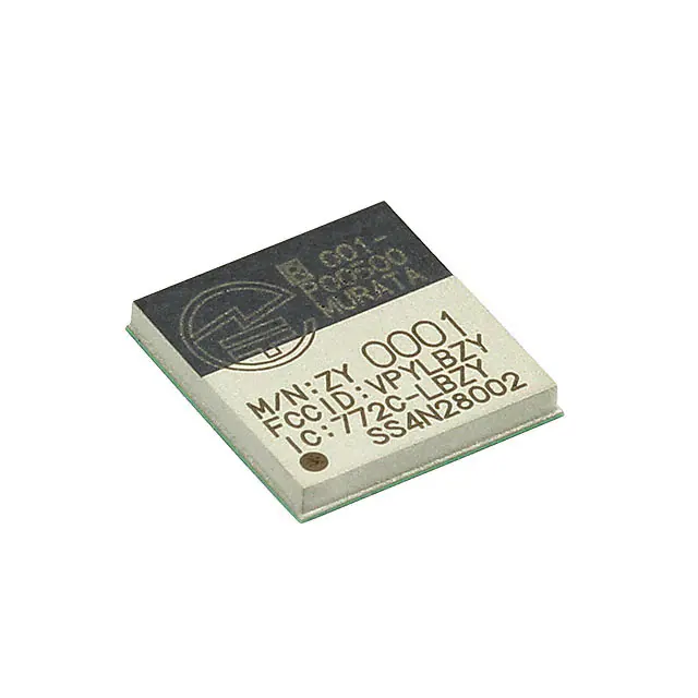
16. Wireless / BT Certification Numbers
This product is certified by following regulation bodies.
- Japanese Radio Law (日本電波法)
Type certification (工事設計認証)
R001-P00500
- FCC (United States) FCC Part 15 subpart C
Limited Modular Approval
FCC ID: VPYLBZY
- IC (Canada) RSS-210
Limited Modular Approval
IC: 772C-LBZY
- CE (Europe) EN 300328 V.2.2.2
Conducted Test Report available
Note: CE marking and declaration should be done by customer as a final product.
- Bluetooth(R) SIG Qualifications
For Bluetooth Specification 4.1
QDID: 56016 (Controller Subsystem by Murata)
QDID: 52696 (Host Subsystem by Dialog)
QDID: 56907 (Profile Subsystem by Dialog)
For Bluetooth Specification 4.2
QDID: 83573 (Controller Subsystem by Dialog)
QDID: 83565 (Host Subsystem by Dialog)
QDID: Ask Dialog or S/W 3rd Party (Profile Subsystem by Dialog)
Note: Profile subsystem QDID is needed only if SIG standard profile is used.
Preliminary
< Specification may be changed by Murata without notice >
Murata Manufacturing Co., Ltd.
�Preliminary Specification Number: SP-HNZY-N
19/22
17. NOTICE
1.Storage Conditions:
Please use this product within 6month after receipt.
- The product shall be stored without opening the packing under the ambient temperature from 5 to
35deg.C and humidity from 20 to 70%RH.
(Packing materials, in particular, may be deformed at the temperature over 40deg.C.)
- The product left more than 6months after reception, it needs to be confirmed the solderbility before
used.
- The product shall be stored in non corrosive gas (Cl2, NH3, SO2, Nox, etc.).
- Any excess mechanical shock including, but not limited to, sticking the packing materials by sharp
object and dropping the product, shall not be applied in order not to damage the packing materials.
This product is applicable to MSL3 (Based on JEDEC Standard J-STD-020)
- After the packing opened, the product shall be stored at
Murata Manufacturing Co., Ltd.
�