W-LAN / LAN Module Data Sheet
Cypress WLAN / LAN Chipset CYW43907
Electric Imp P/N : imp005
MURATA P/N : LBWA1UZ1GC-901
This Datasheet is a preliminary version, and subject
to change without notice.
Preliminary & Confidential
< Specification may be changed by Murata without notice >
Murata Manufacturing Co., Ltd.
�Preliminary Specification
Number : SP-UZ1GC_01-C
1 / 27
The revision history of the product specification
Issued
Date
Dec. 25. 2015
Mar. 18. 2016
Dec. 30. 2016
Revision
Code
Revision
Page
A
P5
P6
P11
P13
P14
P21
B
P3
P4
P7
P11
P12
P13
P16
P17
P18
P19
-
Changed Items
First Issue
Adding Structure
Adding Pin Layout
Revised 6. Operating Condition
Adding 9. Digital I/O Requirements
Revised 10. RF Characteristics
Adding 12. Reference Circuit
Modifying Scope and Part Number
Changing Block diagram.
Updated 4.2. Terminal configurations
Adding 5. LED Drive
Adding 6. Phototransistor
Adding 7. SPI Flash Requirements
Updated 12. Pin characteristics
Updated 13. Land pattern
Updated 14. Reference circuits
Updated 15. Recommended component
Erased RF Characteristics
Preliminary & Confidential
< Specification may be changed by Murata without notice >
Murata Manufacturing Co., Ltd.
Change Reason
Update
Update
�Preliminary Specification
Number : SP-UZ1GC_01-C
2 / 27
TABLE OF CONTENTS
1. Scope .....................................................................................................................................................3
2. Part Number ........................................................................................................................................3
3. Block Diagram ......................................................................................................................................4
4. Dimensions, Marking and Terminal Configurations .........................................................................5
4.1. Dimensions ....................................................................................................................................5
4.2. Terminal Configurations ...............................................................................................................7
5. LED Drive .......................................................................................................................................... 11
6. Phototransistor ..................................................................................................................................12
7. SPI Flash Requirements....................................................................................................................13
8. Absolute Maximum Rating ................................................................................................................14
9. Operating Condition ..........................................................................................................................14
10. External 32.768 kHz Low-Power Oscillator ...................................................................................14
11. Power Up Sequence ..........................................................................................................................15
12. Digital I/O Specifications .................................................................................................................16
13. Land pattern (Top View) ..................................................................................................................17
14. Reference Circuits ............................................................................................................................18
14.1. Module connections ...................................................................................................................18
14.2. Blinkup circuit ...........................................................................................................................19
14.3. Boot flash & status indication ..................................................................................................19
14.4. Antenna ......................................................................................................................................19
14.5. Ethernet 10/100Mbps ................................................................................................................20
15. Recommended Components .............................................................................................................21
15.1. Bi-color LED ..............................................................................................................................21
15.2. Phototransistor ..........................................................................................................................21
15.3. SPI Flash ...................................................................................................................................21
15.4. Blinkup circuit ...........................................................................................................................21
15.5. Ethernet PHY & magnetics ......................................................................................................21
16. Tape and Reel Packing ....................................................................................................................22
17. NOTICE ............................................................................................................................................25
17.1. Storage Conditions: ...................................................................................................................25
17.2. Handling Conditions: ................................................................................................................25
17.3. Standard PCB Design (Land Pattern and Dimensions): ........................................................25
17.4. Notice for Chip Placer: ..............................................................................................................25
17.5. Soldering Conditions: ................................................................................................................26
17.6. Cleaning: ....................................................................................................................................26
17.7. Operational Environment Conditions: .....................................................................................26
17.8. Input Power Capacity: ..............................................................................................................26
18. PRECONDITION TO USE OUR PRODUCTS...............................................................................27
Please be aware that an important notice concerning availability, standard warranty and use in critical
applications of Murata products and disclaimers thereto appears at the end of this specification sheet.
Preliminary & Confidential
< Specification may be changed by Murata without notice >
Murata Manufacturing Co., Ltd.
�Preliminary Specification
Number : SP-UZ1GC_01-C
3 / 27
1. Scope
This specification is for the LBWA1UZ1GC (imp005) module that provides connectivity to the internet
via WiFi or Ethernet.
The device is pre-provisioned with keys to boot impOS – a fully maintained, secure OS that is part of
the Electric Imp cloud service.
•
802.11 a/b/g/n 1x1 WiFi (dual band 2.4GHz & 5GHz)
o 802.11a 13.0dBm +/-2.0dBm
o 802.11b 17.0dBm +/-2.0dBm
o 802.11g 13.0dBm +/-2.0dBm
o 802.11n(5GHz) 12.0dBm +/-2.0dBm (20/40MHz channels)
o 802.11n(2.4GHz) 12.0dBm +/-2.0dBm (20MHz channels)
o RX Sensitivity -97dBm typical (@1Mbps)
o Diversity antenna switch outputs
o Supports WPA, WPA2, WPS
•
10/100MHz Ethernet MAC
o Connects to external RMII Ethernet PHY & magnetics
•
32-bit Cortex R4 application processor
o Secure boot from external QSPI
o 32kB instruction & data caches
o Over 1.2MB RAM for application use
o 256kB of secure application storage on external QSPI
o Secure credential storage on external QSPI
•
Electric Imp OS & service
o Robust embedded operating system with fail-safe & secure OS & application updates
o Pre-provisioned MAC addresses (per interfdace) & per device secrets
o TLS1.2-RSA-ECDHE (forward secrecy) cloud connection
o Elliptic curve challenge-response to prevent device impersonation
o Fully featured cloud VM for every device for easy integration with cloud services
o Open source integrations with AWS, Azure, IBM Watson, etc
•
•
LED drive for red/green status LEDs
Phototransistor input for Electric imp’s patented BlinkUpTM technology
o
Provides secure, replay-proof provisioning from a mobile app or webpage
•
Flexible I/O
o 28x GPIO, configurable to support 1x SPI, 1x I2C and 6xPWM
o Dedicated interfaces: 1x SPI, 1x I2C, 3x UART, 1x USB host
•
Compliant with the RoHS directive
2. Part Number
Sample Part Number
LBWA1UZ1GC-TEMP-IMP
Production Part Number
LBWA1UZ1GC-901
Preliminary & Confidential
< Specification may be changed by Murata without notice >
Murata Manufacturing Co., Ltd.
�Preliminary Specification
Number : SP-UZ1GC_01-C
4 / 27
3. Block Diagram
Preliminary & Confidential
< Specification may be changed by Murata without notice >
Murata Manufacturing Co., Ltd.
�Preliminary Specification
Number : SP-UZ1GC_01-C
5 / 27
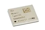
4. Dimensions, Marking and Terminal Configurations
4.1. Dimensions
< Top View >
L
(B)
(D)
(C)
(F)
Model:
Type1GC
W
xxxxxxxxx
(E)
(A)
electricimp
< Bottom View: NOTE THIS IS BOTTOM VIEW >
a3
b3 c2 e4
e5 e6
a4
e7
c3
(D3)(A30)
(A44)(D4)
(A29)
(A45)
(D7)(B20)
(B29)(D8)
e8
c4
e9
(B19) (D11) (C9)
(C14)(D12) (B30)
e10
(C8)
(E12)
(E6)
(E1)
(C7)
e3
a5
e11
(C15)
(E7)
(C16)
c5
a2
(C1) (D9)
(D10)(C6)
(B11)
(A16)
e2
c1
b2
(D6)(B10)
(B1) (D5)
(D2)(A15)
< Side View >
e12
(B38)
(A58)
(A1)(D1)
e1
a1
b1
T
T1
Preliminary & Confidential
< Specification may be changed by Murata without notice >
Murata Manufacturing Co., Ltd.
�Mark
L
T
a1
a4
b1
c1
c4
e1
e4
e7
e10
Dimensions
10.0 +/- 0.2
1.20 max.
0.25 +/- 0.1
0.25 +/- 0.1
0.395 +/- 0.2
0.55+/- 0.1
0.55+/- 0.1
0.31 +/- 0.1
0.932 +/- 0.1
0.882 +/- 0.1
0.31 +/- 0.1
Mark
W
T1
a2
a5
b2
c2
c5
e2
e5
e8
e11
Dimensions
10.0 +/- 0.2
0.07 typ.
0.25 +/- 0.1
0.25 +/- 0.1
0.293 +/- 0.2
0.55+/- 0.1
0.55+/- 0.1
0.392 +/- 0.1
0.31 +/- 0.1
0.858 +/- 0.1
0.45 +/- 0.1
Preliminary Specification
Number : SP-UZ1GC_01-C
6 / 27
Mark
Dimensions
a3
0.25 +/- 0.1
b3
c3
0.313 +/- 0.2
0.55+/- 0.1
e3
e6
e9
e12
0.31 +/- 0.1
0.25 +/- 0.1
0.384 +/- 0.1
0.974+/- 0.1
(unit : mm)
Marking
Marking
(A)
(B)
(C)
(D)
(E)
(F)
Meaning
Pin 1 Marking
Murata Logo
Inspection Number
Module Type
Electric Imp Logo
2D code
Preliminary & Confidential
< Specification may be changed by Murata without notice >
Murata Manufacturing Co., Ltd.
�Preliminary Specification
Number : SP-UZ1GC_01-C
7 / 27
4.2. Terminal Configurations
Pin#
Name
Type
Description
D1
SFLASH_MISO_3
I/O
Flash data bit 4
A1
SFLASH_CLK
O
Flash clock
A2
SFLASH_MOSI_0
I/O
Flash data bit 1
A3
SFLASH_MISO_2
I/O
Flash data bit 3
A4
SFLASH_CS_L
O
Flash slave select
A5
GND
GND
A6
RF_ANT0
I/O
A7
GND
GND
A8
TEST_3V3
I
Tie high
A9
pinB
I/O
GPIO/SPI MOSI (default driven high)
A10
pinD
I/O
GPIO/SPI nCS (default driven high)
A11
pinA
I/O
GPIO/SPI CLK (default driven low)
A12
pinC
I/O
GPIO/SPI MISO
A13
RMII_TXEN
O
RMII Transmit Enable
A14
RMII_CRS_DV
I
Receive Data Valid
A15
RMII_MDC
O
RMII Management Data Clock
D2
RMII_TXD0
O
RMII Transmit Data Output
A16
RMII_RXD0
I
RMII Receive Data Input
A17
RMII_REF_CLK
I
Transmit Clock
A18
RMII_RXD1
I
RMII Receive Data Input
A19
RMII_TXD1
O
RMII Transmit Data Output
A20
RMII_MDIO
I/O
RMII Management Data I/O
A21
ANT1_DIV
O
A22
VDD_3V0_IN
PWR
A23
XTAL32K_IN
I
ANT1 Diversity RF switch control
3.0V input: see design guide, sensitive
trace. Connected to VDD_3V0_OUT.
XTAL input
A24
XTAL32K_OUT
O
XTAL output
A25
ANT0_DIV
O
ANT0 Diversity RF switch control
A26
pinE
I/O
GPIO/PWM (default driven low)
A27
pinF
O
GPIO/PWM (default driven low)
A28
USB2_DN
I/O
USB Host Data Minus
A29
USB2_DP
I/O
USB Host Data Plus
D3
GND
GND
A30
n/c
n/c
A31
pinG
O
GPIO/PWM (default driven low)
A32
TEST_GND
I
Tie low
A33
GND
GND
A34
USB_VDD_3V3
PWR
3.3V supply for USB
A35
VDD_3V3_IN_2
PWR
3.3V input
A36
GND
GND
A37
VDDIO
PWR
Antenna port 0
I/O supply
Preliminary & Confidential
< Specification may be changed by Murata without notice >
Murata Manufacturing Co., Ltd.
�Preliminary Specification
Number : SP-UZ1GC_01-C
8 / 27
A38
GND
GND
A39
VDD_3V0_OUT
PWR
A40
GND
GND
A41
DCDC_IN
PWR
A42
GND
GND
A43
VDD
PWR
Main power input (VBAT)
A44
DCDC_OUT
PWR
PMU CBUCK Switching Regulator Out
D4
GND
GND
A45
pinH
I/O
GPIO
A46
pinK
I/O
GPIO/i2cJK SDA (default driven high)
A47
pinJ
I/O
GPIO/i2cJK SCL (default driven low)
A48
n/c
n/c
A49
pinM
I/O
GPIO
A50
BLINKUP_DIN
I
Blinkup data input
A51
BLINKUP_EN_L
O
Blinkup power enable (high = on)
A52
UART0_RXD
I
uart0 serial input
A53
UART0_RTS
O
uart0 request-to-send
A54
UART0_CTS
I
uart0 clear-to-send
A55
UART0_TXD
O
uart0 serial output
A56
VDDIO_3V3
PWR
I/O supply
A57
VDDIO_3V3
PWR
I/O supply for RMII
A58
SFLASH_MISO_1
I/O
Flash data bit 2
D5
n/c
n/c
B1
pinL
I/O
GPIO
B2
I2C0_SCL
I/O
i2c0 SCL
B3
GND
GND
B4
pinXA
I/O
B5
n/c
n/c
B6
n/c
n/c
B7
n/c
n/c
B8
n/c
n/c
B9
n/c
n/c
B10
n/c
n/c
D6
n/c
n/c
B11
GND
GND
B12
RESET_L
I
B13
HIB_WAKE_L
I
B14
UART1_RXD
I
B15
UART1_TXD
O
B16
n/c
n/c
B17
TEST_GND
I
3.0V output of internal LDO
Input to internal PMU LDO
GPIO/WAKE
Reset (not recommended for chip reset,
see PWR_DWN_L)
Pull-up to 3v3
uart1 RXD (default driven low: note, use
series resistor to limit current at boot)
uart1 RXD
Tie low
Preliminary & Confidential
< Specification may be changed by Murata without notice >
Murata Manufacturing Co., Ltd.
�B18
UART2_RXD
I
B19
pinR
I/O
Preliminary Specification
Number : SP-UZ1GC_01-C
9 / 27
uart2 RXD (default driven low: note, use
series resistor to limit current at boot)
GPIO/USB_PWR_EN
D7
pinS
I/O
GPIO/PWM (default driven low)
B20
pinXB
I/O
GPIO/WAKE
B21
n/c
I/O
n/c
B22
n/c
I/O
n/c
B23
n/c
I/O
n/c
B24
n/c
I/O
n/c
B25
n/c
I/O
n/c
B26
n/c
I/O
n/c
B27
n/c
I/O
n/c
B28
GND
GND
B29
GND
GND
D8
pinT
I/O
GPIO
B30
SPI0_MOSI
O
spi0 SPI data master out
B31
SPI0_MISO
I
spi0 SPI data master in
B32
SPI0_CLK
O
spi0 SPI clock
B33
SPI0_CS_L
O
spi0 SPI slave select
B34
GND
GND
B35
Red LED
O
B36
Green LED
O
Red LED drive (CA/CC – fit 10k resistor
across red LED for CA/CC detect)
Green LED drive (CA/CC)
B37
pinQ
I/O
GPIO (default driven low)
B38
pinP
I/O
GPIO
D9
GND
GND
C1
I2C0_SDA
I/O
i2c0 SDA
C2
pinXC
I/O
GPIO/WAKE
C3
pinXD
I/O
GPIO/WAKE
C4
n/c
n/c
C5
PWR_DWN_L
I
C6
TEST_GND
I
D10
GND
GND
C7
UART2_TXD
O
C8
GND
GND
D11
GND
GND
C9
pinU
I/O
GPIO/PWM (default driven low)
C10
pinV
I/O
GPIO/PWM (default driven low)
C11
pinW
I/O
GPIO/USB fault indication
C12
VDDIO_3V3
PWR
I/O supply
C13
pinXE
I/O
GPIO/WAKE
C14
pinY
I/O
GPIO
Pull low to power chip down. Pull high to
wake chip up. Use in preference to
RESET_L if chip reset is desired
Tie low
uart2 TXD
Preliminary & Confidential
< Specification may be changed by Murata without notice >
Murata Manufacturing Co., Ltd.
�Preliminary Specification
Number : SP-UZ1GC_01-C
10 / 27
D12
GND
GND
C15
TEST_3V3
I
Tie high
C16
pinN
I/O
GPIO
E1
GND
GND
E2
GND
GND
E3
GND
GND
E4
GND
GND
E5
GND
GND
E6
GND
GND
E7
GND
GND
E8
GND
GND
E9
GND
GND
E10
GND
GND
E11
GND
GND
E12
GND
GND
Preliminary & Confidential
< Specification may be changed by Murata without notice >
Murata Manufacturing Co., Ltd.
�Preliminary Specification
Number : SP-UZ1GC_01-C
11 / 27
5. LED Drive
The indicator LED should be bicolor, because red, green and amber (red+green) are used to indicate
status.
The LED drive pins will auto-detect common anode or common cathode parts. The detection is done by
looking to see which way up the LED_RED pin is idling at boot; to ensure this works correctly, please
place a 10k resistor in parallel with the red LED.
The current drive on these pins is 8mA maximum.
Please refer to section 15 for the recommended LEDs.
Two specific LED codes indicate errors when talking to the SPI flash:
SPI flash not found
SPI flash error
If you encounter either of these codes, then this indicates an electrical connection issue or an
incompatible flash part.
Preliminary & Confidential
< Specification may be changed by Murata without notice >
Murata Manufacturing Co., Ltd.
�Preliminary Specification
Number : SP-UZ1GC_01-C
12 / 27
6. Phototransistor
The phototransistor is used to receive BlinkUp configuration data. Unlike other imps, the imp005 does
not have an on-board ADC, so an external ramp ADC circuit is used to capture the light levels. This
circuit feeds a pulse train into the imp where it is interpreted by software.
Sensitivity is tuned by adjusting C7 – a smaller capacitor increases sensitivity. Typically, the value used
will range between 470pF and 4700pF, and the value should only be picked when the final optical path
is available for testing. Please see the section on tuning blinkup on www.electricimp.com. Note that a
C0G capacitor with 5% or better tolerance is recommended to reduce unit to unit variation.
The components used here have been chosen to be easily available and low cost. U2 is a simple
comparator which triggers when the voltage on C7 rises to above 0.5xVDD, and R12/C12 and U4 give
a fixed length pulse at the start of every slot, turning on Q2 to drain C7.
If the application is not power sensitive, Q1/R9 can be removed, connecting 3V3_BU directly to the
main 3V3 rail.
End-user BlinkUp sends data at between 30 and 60 bits per second, depending on the user’s device.
For factory configuration, data is typically sent at 142 bits per second using red LED(s) in a test fixture.
If your application does not require optical configuration, config can be sent electrically at 142 bits per
second from another micro using the OPTO_IN pin. Please contact us for more details.
Please refer to section 15 for recommended phototransistors.
Preliminary & Confidential
< Specification may be changed by Murata without notice >
Murata Manufacturing Co., Ltd.
�Preliminary Specification
Number : SP-UZ1GC_01-C
13 / 27
7. SPI Flash Requirements
An external SPI Flash part is required for operation.
Minimum Size
32 Mbit (4 MByte)
Reserved for OS (must be pre-programmed)
0x000000 to 0x35E000 (3448 kByte)
The minimum size of the SPI Flash is 32Mbit (4MB), and the maximum size is 128Mbit (16MB). The
area below address 0x35E000 (3448kB) is reserved for use by the OS. The remainder of the flash
device is made available to user code programmatically, and may optionally be pre-programmed for
user applications before assembly.
The imp005’s SPI flash chip must support both 4KB and 64KB erases (command 0x20 and 0xD8) and
Page Program (command 0x02).
Though the imp005 always boots in single bit mode, it will move to QSPI if this is enabled via the device
configuration page within flash. See the imp005 hardware design guide for more information on the
device configuration page.
We recommend fitting 22R source termination resistors near the imp005 (for SCLK & MOSI/IO0) and
the flash (for MISO/IO1, nWP/IO2 and HOLD/IO3).
The OS image must be loaded onto the flash before the device will operate
This can be done before SMT, or in-circuit by asserting the PWR_DWM_L signal and driving the SPI
bus directly; the imp005 breakout board exposes the necessary pins for this on a 0.1” header. The
public cloud OS image is available for download from the imp005 design section of
www.electricimp.com
Note that the imp005, unlike the Murata 1GC, is pre-loaded with AES & RSA keys that will only accept
firmware images signed by Electric Imp’s FIPS140-2 HSM. It is not possible to run generic WICED
software on this part.
Preliminary & Confidential
< Specification may be changed by Murata without notice >
Murata Manufacturing Co., Ltd.
�Preliminary Specification
Number : SP-UZ1GC_01-C
14 / 27
8. Absolute Maximum Rating
min.
-40
-0.5
-0.5
-0.5
-0.5
-0.5
-0.5
-0.5
Storage Temperature
VDD_VBAT
VDD1_35
USB_VDD_3V3
VDDIO
VDDIO_AUDIO
VDDIO_RMII
VDDIO_SD
Supply Voltage
max.
85
5.5
1.5
3.9
3.9
3.9
3.9
3.9
unit
deg.C
V
V
V
V
V
V
V
Stresses in excess of the absolute ratings may cause permanent damage. Functional operation is not implied under
these conditions. Exposure to absolute ratings for extended periods of time may adversely affect reliability. No
damage assuming only one parameter is set at limit at a time with all other parameters is set within operating condition.
9. Operating Condition
Operating Temperature Range(*1)
Specification Temperature Range
VDD_VBAT
VDD1_35
USB_VDD_3V3
Supply Voltage
VDDIO
VDDIO_AUDIO
VDDIO_RMII
VDDIO_SD
min.
-30
-20
3.13
1.3
2.97
2.97
1.71
1.71
1.71
typ.
1.35
3.3
3.3
max.
70
70
4.8
1.5
3.63
3.63
3.63
3.63
3.63
unit
deg.C
deg.C
V
V
V
V
V
V
V
[Note] All RF characteristics in this datasheet are defined by Specification Temperature Range. Default configuration
of VDD_3V3_IN and VDD_3V3_IN2 is to connect with VDD_3V3_LDO. Specifications require derating at
extreme temperatures.
10. External 32.768 kHz Low-Power Oscillator
This module uses a secondary low frequency clock for low-power mode timing.
Parameter
Normal Input Frequency
Frequency Accuracy
Duty Cycle
Input Signal Amplitude
Signal Type
Input Impedance1)
Clock Jitter (During Initial Start-up)
1) When power is applied or switched off.
LPO Clock
32.768
+/-200
30 – 70
200 – 3300
Square-wave, or Sine-wave
>100k
Murata Manufacturing Co., Ltd.
unit
kHz
ppm
%
mVp-p
Ohm
pF
ppm
�Preliminary Specification
Number : SP-UZ1GC_01-C
15 / 27
11. Power Up Sequence
Following timing diagram explain module power up sequence.
32.768kHz Sleep Clock
VBAT
VDDIO
~2 Sleep Cycles
HIB_REG_ON_IN
*Power down sequence is opposite sequence of power up.
Note: The CYW43907 has an internal power-on-reset (POR) circuit. The device will be held in reset for
a maximum of 110 ms after VDDC (internal LDO output) and VDDIO have both passed the POR
threshold.
Note: The 10% - 90% VBAT rise time should not be faster than 40 microseconds. VBAT should be up
before or at the same time as VDDIO. VDDIO should not be present first or be held high before VBAT is
high.
Preliminary & Confidential
< Specification may be changed by Murata without notice >
Murata Manufacturing Co., Ltd.
�Preliminary Specification
Number : SP-UZ1GC_01-C
16 / 27
12. Digital I/O Specifications
All specifications are at 3.3v.
Digital I/O Pins
Input high voltage
Input low voltage
Output high voltage@2mA
Output low voltage@2mA
Sym
VIH
VIL
VOH
VOL
min.
2.00
VDDIO-0.4
-
typ.
-
max.
0.80
0.40
unit
V
V
V
V
RF Switch control Output Pins
Output high voltage@2mA
Output low voltage@2mA
Input capacitance
Sym
VOH
VOL
CIN
min.
VDDIO-0.4
-
typ.
-
max.
0.4
5
unit
V
V
pF
GPIO, SPI, UART interfaces
Input high voltage
Input low voltage
Output high voltage@2mA
Output low voltage@2mA
Sym
VIH
VIL
VOH
VOL
min.
2.0
-0.5
2.4
-
typ.
-
Preliminary & Confidential
< Specification may be changed by Murata without notice >
Murata Manufacturing Co., Ltd.
max.
VDDIO+0.5
0.8
0.4
unit
V
V
V
V
�Preliminary Specification
Number : SP-UZ1GC_01-C
17 / 27
13. Land pattern (Top View)
5.00
4.605
Unit : mm
4.355
4.045
Note: schematic and footprint
symbols are available from Electric
Imp for Altium & Eagle CAD
packages.
3.795
3.485
3.235
2.925
2.675
2.365
2.115
1.805
1.555
1.245
0.995
0.685
0.435
It is strongly recommended that you
use these fully validated symbols in
your design where possible.
0.125
0.155
0.125
5.00
5.00
4.707
4.157
3.765
3.515
3.205
2.955
2.645
2.395
2.085
1.835
1.525
1.275
0.965
0.715
0.405
PADSTACK INFORMATION
5.00
0.350
0.225
0.435 0.775
0.685 1.225
0.995
1.775
1.245
1.555
1.805
2.115
2.365
2.749
3.299
5.00
0.125
0.155 0.375
0.405 0.625
0.715 0.875
0.965
1.125
1.275
1.375
1.625
1.525
1.875
1.835
2.085
2.395
0.650
SOLDERMASK
(SOLDER REGIST)
2.645
3.205
0.250
5.00
0.250
2.955
0.550
0.550
PIN
SOLDER PASTE
(STENCIL)
Note: For PINs on the board that have a copper pour (flood) associated with it, usually the case with
Ground PINs, please assure that the Land Pattern (PCB Footprint) for these PINs becomes Solder
Mask Defined (SMD). In other words, the SOLDERMASK (SOLDER RESIST) for these Ground (GND)
pins should be 0.550 mm x 0.250 mm (basically SODLERMASK (SOLDER RESIST) becomes same
size as the PIN).
Preliminary & Confidential
< Specification may be changed by Murata without notice >
Murata Manufacturing Co., Ltd.
�Preliminary Specification
Number : SP-UZ1GC_01-C
18 / 27
14. Reference Circuits
The Altium source files for many imp005-based designs are freely downloadable from
www.electricimp.com in the imp005 design section. It’s strongly recommended that new designs copy
as much as possible from these reference designs.
14.1. Module connections
Preliminary & Confidential
< Specification may be changed by Murata without notice >
Murata Manufacturing Co., Ltd.
�Preliminary Specification
Number : SP-UZ1GC_01-C
19 / 27
14.2. Blinkup circuit
14.3. Boot flash & status indication
14.4. Antenna
When the Murata reference PCB antenna is used appropriately in your application, you may be able to
reuse the FCC/IC modular approval of the type 1GC/imp005 module. Please contact Electric Imp for
more details.
Preliminary & Confidential
< Specification may be changed by Murata without notice >
Murata Manufacturing Co., Ltd.
�Preliminary Specification
Number : SP-UZ1GC_01-C
20 / 27
14.5. Ethernet 10/100Mbps
Take care when routing the RMII bus as it runs at 50MHz. See the imp005 breakout reference design for
more information.
Example designs including PoE receivers are also available from Electric Imp.
Preliminary & Confidential
< Specification may be changed by Murata without notice >
Murata Manufacturing Co., Ltd.
�Preliminary Specification
Number : SP-UZ1GC_01-C
21 / 27
15. Recommended Components
15.1. Bi-color LED
Manufacturer
Manufacturer’s part number
SunLED
Liteon
SunLED
Bivar
XZMDKVG59W-1
LTST-C195KGJRKT
XZMDKVG88W
SM1204BC
SunLED
Liteon
XLMDKVG34M
LTL1BEKVJNN
Manufacturer
Manufacturer’s part number
Everlight
Fairchild
SunLED
Everlight
PT17-21C/L41/TR8
KDT00030TR
XZRNI56W-1
PT12-21C/TR8
SunLED
LiteOn
XRNI30W-1
LTR-4206
Manufacturer
Cypress
Cypress
Winbond
Manufacturer’s part number
S25FL132K
S25FL164K
W25Q128JV
Surface mount
top-view
side-view
Through-hole
3mm
15.2. Phototransistor
Surface mount
top-view
side-view
Through-hole
3mm
15.3. SPI Flash
Size
32 Mbit
64 Mbit
128 Mbit
Note: Cypress 128Mbit S25FL127/128 parts are not compatible because they do not offer a uniform 4k
erase size across the flash area.
15.4. Blinkup circuit
Part
Comparator, open-drain
Schmitt inverter
Manufacturer
Diodes Inc
Diodes Inc
Manufacturer’s part number
AP331AWG-7
74LVC1G14W5-7
Manufacturer
Microchip
Stewart Connector
Manufacturer’s part number
LAN8720A-CP-TR
SI-50170-F
15.5. Ethernet PHY & magnetics
Part
10/100 Ethernet PHY
RJ45 Magjack with LEDs
Preliminary & Confidential
< Specification may be changed by Murata without notice >
Murata Manufacturing Co., Ltd.
�Preliminary Specification
Number : SP-UZ1GC_01-C
22 / 27
16. Tape and Reel Packing
2.0±0.1
4.0±0.1
f 1.5+0.1/-0.0
0.30±0.05
11.5±0.1
10.5±0.1
24.0±0.3/-0,1
1.75±0.10
(1) Dimensions of Tape (Plastic tape)
f 1.5±0.1/-0.0
16.0±0.1
10.5±0.1
1.7 max.
(1.6±0.1)
feeding direction
The corner and ridge radiuses (R) of inside cavity are 0.3mm max.
Cumulative tolerance of 10 pitches of the sprocket hole is +/-0.2mm
Measuring of cavity positioning is based on cavity center in accordance with JIS/IES standard.
(2) Dimensions of Reel
25.5±0.6
( f 330)
2.0±0.5
( f 100)
1)
2)
3)
f 13±0.2
30.5 max.
(unit : mm)
Preliminary & Confidential
< Specification may be changed by Murata without notice >
Murata Manufacturing Co., Ltd.
�Preliminary Specification
Number : SP-UZ1GC_01-C
23 / 27
(3) Taping Diagrams
[1] Feeding Hole : As specified in (1)
[2] Hole for chip : As specified in (1)
[3] Cover tape
: 62μm in thickness
[4] Base tape
: As specified in (1)
[3]
[1]
[2]
[3]
[4]
Feeding Hole
Feeding Direction
Pin 1 Marking
Chip
(4) Leader and Tail tape
Feeding direction
Tail tape
(No components)
40 to 200mm
Components
No components
Leader tape
(Cover tape alone)
150mm min.
250mm min.
Preliminary & Confidential
< Specification may be changed by Murata without notice >
Murata Manufacturing Co., Ltd.
�Preliminary Specification
Number : SP-UZ1GC_01-C
24 / 27
(5) The tape for chips are wound clockwise, the feeding holes to the right side as the tape is pulled
toward the user.
(6) The cover tape and base tape are not adhered at no components area for 250mm min.
(7) Tear off strength against pulling of cover tape : 5N min.
(8) Packaging unit : 1000pcs./ reel
(9) material : Base tape : Plastic
Real
: Plastic
Cover tape, cavity tape and reel are made the anti-static processing.
(10) Peeling of force : 1.1N max. in the direction of peeling as shown below.
1.1 N max.
165 to 180 °
Cover tape
Base tape
(11) Packaging (Humidity proof Packing)
Label
表示ラべル
Desiccant
乾燥剤
Humidity
湿度
Indicator
インジケ-タ
表示ラベル
Label
防湿梱包袋
Anti-humidity
Plastic Bag
Tape and reel must be sealed with the anti-humidity plastic bag. The bag contains the desiccant
and the humidity indicator.
Preliminary & Confidential
< Specification may be changed by Murata without notice >
Murata Manufacturing Co., Ltd.
�Preliminary Specification
Number : SP-UZ1GC_01-C
25 / 27
17. NOTICE
17.1. Storage Conditions:
Please use this product within 6month after receipt.
- The product shall be stored without opening the packing under the ambient temperature from 5 to
35deg.C and humidity from 20 to 70%RH.
(Packing materials, in particular, may be deformed at the temperature over 40deg.C.)
- The product left more than 6months after reception, it needs to be confirmed the solderbility before used.
- The product shall be stored in non corrosive gas (Cl2, NH3, SO2, Nox, etc.).
- Any excess mechanical shock including, but not limited to, sticking the packing materials by sharp object
and dropping the product, shall not be applied in order not to damage the packing materials.
This product is applicable to MSL3 (Based on JEDEC Standard J-STD-020)
- After the packing opened, the product shall be stored at
Murata Manufacturing Co., Ltd.
�