Specification Number : SP-ZV1CD-J
WiFi Module Data Sheet
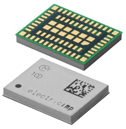
Cypress BCM43362 WiFi + ST Micro STM32F405 MCU
Electric Imp P/N : imp003
MURATA P/N : LBWA1ZV1CD-716
< Specification may be changed by Murata without notice >
Murata Manufacturing Co., Ltd.
�
Specification Number : SP-ZV1CD-J
1 / 24
Revision history
Issued
Date
Apr.11.2014
May.23.2014
Jun.3.2014
Revision
Code
A
Revision
Page
P4
P10
B
P17
P9
P11
Jul.1.2014
C
P12
P18
P10
Jul.31.2014
D
Oct.14.2014
E
P18
Jun.8.2015
F
P18
Jan.21.2016
G
P18
P5
P11
P13,14
Apr.26.2016
H
P16
Oct.13.2016
I
P9, 10,
11, 18
Oct.20.2016
J
Changed Items
First issued
3. Block Diagram, 2MBit -> 4MBi
7. Absolute Maximum Rating
8. Operating Condition
9. Electric characteristics
14. Recommended Components
5. LED Drive
6. Phototransistor
Corrected reference paragraph
10. External clock source
characteristics add
11. Power Up Sequence
Changed "NRST" to "RESET_L"
15.4. Low Power Schematic
-ABS07-120-32.768kHz-T add
-Changed "ST3215SB32768B0HPWB1"
to "ST3215SB32768B0HPWB3"
7. SPI Flash Requirements
Added SPI Flash Requirements
16. Recommended Components
Added SPI Flash
16. Recommended Components
-Changed APT2012P3BT with KDT00030TR
-Changed S24FLxxx with S25FLxxx
16.5. Low Power Schematic
-Changed "AP2281" to " AP2281-1/AP2281-3"
-Changed "ABS25-32.768KHZ-T"
to "ABS25-32.768KHZ-6-T "
4.1. Dimensions
-add marking information
11. Electric characteristics
-updated
13. RF Characteristics
-updated current consumption
15. Reference Circuit
-Corrected
5. LED
- add failure codes
6. Phototransistor
- add RF coupling capacitor recommendation
7. SPI flash
- add more detail on compatible flash types
15.1. Low Cost schematic
- connected OSC32_IN to GND
16.2. Phototransistor
Remove RF characteristics section, add typical
specs. Update cloud description
< Specification may be changed by Murata without notice >
Murata Manufacturing Co., Ltd.
Change
Reason
�
Specification Number : SP-ZV1CD-J
2 / 24
TABLE OF CONTENTS
1. Scope ....................................................................................................................................................3
2. Part Number ..........................................................................................................................................3
3. Block Diagram .......................................................................................................................................4
4. Dimensions, Marking and Terminal Configurations ...............................................................................5
4.1. Dimensions .....................................................................................................................................5
4.2. Terminal Configurations ..................................................................................................................6
4.3. Pin Mux Table .................................................................................................................................8
5. LED Drive ..............................................................................................................................................9
6. Phototransistor ....................................................................................................................................10
7. SPI Flash Requirements ..................................................................................................................... 11
8. Absolute Maximum Ratings ................................................................................................................. 11
9. Operating Conditions ........................................................................................................................... 11
10. Electrical characteristics ....................................................................................................................12
11. External clock source characteristics .................................................................................................12
11.1. Low-speed external user clock characteristics............................................................................12
12. Power Up Sequence .........................................................................................................................13
12.1. Without RESET_L control ...........................................................................................................13
12.2. With RESET_L control ................................................................................................................13
12.2.1. RESET_L Circuit ..................................................................................................................13
13. Land Pattern (Top View) ....................................................................................................................14
14. Reference Circuit ...............................................................................................................................15
14.1. Low Cost Schematic ...................................................................................................................15
14.2. Low Power Schematic ................................................................................................................16
15. Recommended Components .............................................................................................................17
15.1. Bi-color LED ................................................................................................................................17
15.2. Phototransistor ............................................................................................................................17
15.3. SPI Flash ....................................................................................................................................17
15.4. Low Cost Schematic ...................................................................................................................17
15.5. Low Power Schematic ................................................................................................................17
16. Tape and Reel Packing......................................................................................................................18
17. NOTICE .............................................................................................................................................21
17.1. Storage Conditions: ....................................................................................................................21
17.2. Handling Conditions: ...................................................................................................................21
17.3. Standard PCB Design (Land Pattern and Dimensions): .............................................................21
17.4. Notice for Chip Placer: ................................................................................................................21
17.5. Soldering Conditions: ..................................................................................................................22
17.6. Cleaning: .....................................................................................................................................22
17.7. Operational Environment Conditions: .........................................................................................22
17.8. Input Power Capacity: .................................................................................................................22
18. PRECONDITION TO USE OUR PRODUCTS ..................................................................................23
Please be aware that an important notice concerning availability, standard warranty and use in critical
applications of Murata products and disclaimers thereto appears at the end of this specification sheet.
< Specification may be changed by Murata without notice >
Murata Manufacturing Co., Ltd.
�
Specification Number : SP-ZV1CD-J
3 / 24
1. Scope
This specification is for the LBWA1ZV1CD (imp003) module that provides connectivity to the internet
via WiFi. The fully maintained, secure OS that is part of the Electric Imp cloud service comes
pre-loaded.
•
802.11 b/g/n 1x1 WiFi
802.11b 17.0dBm +/-2.0dBm
802.11g 13.0dBm +/-2.0dBm
802.11n 12.0dBm +/-2.0dBm (20MHz channels)
RX Sensitivity -94dBm typical (@1Mbps)
Diversity antenna switch outputs
Supports WEP, WPA, WPA2, WPS
•
32-bit Cortex M4 processor
- Robust embedded operating system with fail-safe firmware updates
- Virtual machine for customer firmware
- 256kB of application bytecode flash
- Around 130kB of dedicated application RAM
•
Electric Imp OS & service
- Robust embedded operating system with fail-safe, secure OS & application updates
- Pre-provisioned MAC address & per-device secrets
- TLS1.2-RSA-ECDHE (forward secrecy) connection to cloud
- Elliptic curve challenge-response to prevent device impersonation
- Fully featured cloud VM for every device for easy integration with RESTful APIs
- Open source integrations with AWS, Azure, etc services
•
LED drive for red/green status LEDs
•
Phototransistor input for Electric imp’s patented BlinkUpTM technology for easy configuration
from any smartphone, tablet, or web browser
•
23 user selectable I/Os
- GPIO, PWM, Analog input & output, SPI, UART, I2C
- Dedicated SPI bus for local storage
•
Low power 4uA sleep mode (with external load switch)
- Option for coin cell RTC battery backup
•
Compliant with the RoHS directive
2. Part Number
Sample Part Number
LBWA1ZV1CD-TEMP
Production Part Number
LBWA1ZV1CD-716
< Specification may be changed by Murata without notice >
Murata Manufacturing Co., Ltd.
�Specification Number : SP-ZV1CD-J
4 / 24
3. Block Diagram
antenna
3.3V switch power supply
4Mbit or higher density
SPI Flash
Load switch
opto
BCM43362
STM32F405
SPDT
LPF
23
I/Os
26MHz
xtal
26MHz
xtal
LBWA1ZV1CD-716
32.768KHz
xtal
DC/DC
inductor
antenna
4Mbit SPI
Flash
3.3V LDO
opto
BCM43362
STM32F405
SPDT
LPF
23
I/Os
26MHz
xtal
26MHz
xtal
LBWA1ZV1CD-716
DC/DC
inductor
< Specification may be changed by Murata without notice >
Murata Manufacturing Co., Ltd.
�Specification Number : SP-ZV1CD-J
5 / 24
4. Dimensions, Marking and Terminal Configurations
4.1. Dimensions
< Top View >
< Bottom View >
< Side View >
L
e7
T
23
(B)
(F)
24
a5 e8
25
26
27
28
29
30
31
32
33
34
55
56
57
58
59
60
61
62
63
64
35
22
37
20
(C)
18
xxxxxxxxx
(A)
39
19
W
(E)
71
72
73
74
75
76
70
69
68
67
66
65
40
41
m2
17
m1
16
electricimp
e6
a4
e5
15
c2
14
54
53
52
51
50
49
48
47
46
42
43
45
44
13
12
11
10
9
8
7
6
5
4
3
2
1
b2
c1
Mark
L
a1
a4
b2
c3
e1
e4
e7
e10
Dimensions
10.0 +/- 0.2
0.65 +/- 0.1
0.35 +/- 0.1
0.30 +/- 0.2
0.80 +/- 0.1
0.30 +/- 0.1
0.80 +/- 0.1
0.75 +/- 0.1
0.60 +/- 0.1
Mark
W
a2
a5
c1
c4
e2
e5
e8
m1
Dimensions
7.9 +/- 0.2
0.35 +/- 0.1
0.80 +/- 0.1
0.80 +/- 0.1
0.80 +/- 0.1
0.30 +/- 0.1
0.40 +/- 0.1
0.30 +/- 0.1
0.40 +/- 0.1
e4 a3 e3
e2 a2 e1 a1 b1
Mark
T
a3
b1
c2
c5
e3
e6
e9
m2
Dimensions
1.25 max.
0.35 +/- 0.1
0.30 +/- 0.2
0.80 +/- 0.1
0.80 +/- 0.1
0.30 +/- 0.1
0.30 +/- 0.1
0.50 +/- 0.1
0.40 +/- 0.1
(unit : mm)
Marking
Marking
(A)
(B)
(C)
(D)
(E)
(F)
c3
e9
c4
38
21
(D)1CD
36
Meaning
Pin 1 Marking
Murata Logo
Inspection Number
Module Type
Electric Imp Logo
2D code
< Specification may be changed by Murata without notice >
Murata Manufacturing Co., Ltd.
e10
c5
�
Specification Number : SP-ZV1CD-J
6 / 24
4.2. Terminal Configurations
No.
Terminal Name
Type
1
GND
-
Ground
2
OPTO_BIAS
O
Phototransistor bias voltage
3
OPTO_IN
I
Phototransistor input
4
PinW
5
OSC32_IN
I
MCU sleep clock input
6
OSC32_OUT
O
MCU sleep clock output
7
PinN
I/O
I/O, please refer to Pin mux table
8
PSU_EN
O
External power supply enable
9
WLAN_POWER_EN
O
External power gate enable
10
GND
-
Ground
11
GND
-
Ground
12
ANT
-
Antenna
13
GND
-
Ground
14
GND
-
Ground
15
VDD
PI
16
WLAN_ANT_CTL2
O
17
WLAN_ANT_CTL1
O
18
VDD_PA
PI
I/O
Description
I/O, please refer to Pin mux table
Power supply for MCU VDD and WLAN Digital IO
Antenna switch control. Default is low.
NC if not in use.
Antenna switch control. Default is high.
NC if not in use.
Power supply for Internal Power Amplifier.
19
VDD_PA
PI
20
VDD_WLAN
PI
21
VDD_WLAN
PI
22
VDD_DCDC_IN
PI
23
GND
24
VDD_DCDC_OUT
25
SPIFLASH_NCS
O
SPI flash nCS
26
SPIFLASH_MISO
I
SPI flash MISO
Power supply for WLAN IC
PO
Voltage input for core LDO, low noise LDO1 and
VCO/LDO
Ground
Voltage output for core LDO.
< Specification may be changed by Murata without notice >
Murata Manufacturing Co., Ltd.
�
Specification Number : SP-ZV1CD-J
7 / 24
27
SPIFLASH_MOSI
O
SPI flash MOSI
28
SPIFLASH_SCK
O
SPI flash CLK
29
LED_RED
O
30
LED_GREEN
O
31
PinM
I/O
I/O, please refer to Pin mux table
32
PinL
I/O
I/O, please refer to Pin mux table
33
PinK
I/O
I/O, please refer to Pin mux table
34
PinJ
I/O
I/O, please refer to Pin mux table
35
PinH
I/O
I/O, please refer to Pin mux table
36
GND
-
37
PinG
I/O
I/O, please refer to Pin mux table
38
PinF
I/O
I/O, please refer to Pin mux table
39
PinE
I/O
I/O, please refer to Pin mux table
40
PinD
I/O
I/O, please refer to Pin mux table
41
PinC
I/O
I/O, please refer to Pin mux table
42
PinB
I/O
I/O, please refer to Pin mux table
43
PinA
I/O
I/O, please refer to Pin mux table
44
VDDA
PI
MCU analog power and reference, must be connected to
VDD
45
VBAT
PI
MCU retention RAM and RTC backup supply
46
PinY
I/O
I/O, please refer to Pin mux table
47
GND
-
48
PinV
I/O
49
GND
-
Ground
50
DNC
-
Do not connect
51
GND
-
Ground
52
RESET_L
I
MCU reset, internally pulled up
53
GND
-
Ground
54
GND
-
Ground
Must be connected to the Red terminal of the indicator
LED
Must be connected to the Green terminal of the indicator
LED
Ground
Ground
I/O, please refer to Pin mux table
< Specification may be changed by Murata without notice >
Murata Manufacturing Co., Ltd.
�Specification Number : SP-ZV1CD-J
8 / 24
55
GND
-
Ground
56
GND
-
Ground
57
GND
-
Ground
58
PinQ
I/O
I/O, please refer to Pin mux table
59
PinR
I/O
I/O, please refer to Pin mux table
60
PinT
I/O
I/O, please refer to Pin mux table
61
PinP
I/O
I/O, please refer to Pin mux table
62
PinS
I/O
I/O, please refer to Pin mux table
63
PinU
I/O
I/O, please refer to Pin mux table
64
PinX
I/O
I/O, please refer to Pin mux table
65
VSSA
-
MCU analog ground, must be connected to GND
6676
GND
-
Ground
4.3. Pin Mux Table
Pin
Pin A
Pin B
Pin C
Pin D
Pin E
Pin F
Pin G
Pin H
Pin J
Pin K
Pin L
Pin M
Pin N
Pin P
Pin Q
Pin R
Pin S
Pin T
Pin U
Pin V
Pin W
Pin X
Pin Y
uartFG uartQRPW
uartUVGD
uartWJ uartDM i2cFG i2cAB
SCL
SDA
CTS
spiEBCA
spiLGDK ADC DAC PWM
nSS
MISO
SCLK
TX
yes
yes
yes
SCL
SDA
RTS
yes
yes
yes
yes
SCLK
MOSI
TX
RX
Wake from
sleep
yes
yes
yes
yes
MISO
RX
nSS
MOSI
State
change
callback
yes
yes
yes
yes
yes
yes
yes
yes
yes
yes
RTS
TX
RX
yes
yes
yes
TX
RX
TX
for C
for K,X
yes
yes
yes
yes
RX
CTS
Pin trig
pulse gen
yes
< Specification may be changed by Murata without notice >
Murata Manufacturing Co., Ltd.
yes
yes
yes
yes
yes
yes
for G
for D
�
Specification Number : SP-ZV1CD-J
9 / 24
5. LED Drive
The indicator LED should be bicolor, because red, green and amber (red+green) are used to indicate
status.
The LED drive pins will auto-detect common anode or common cathode parts. The detection is done by
looking to see which way up the LED_RED pin is idling at boot; to ensure this works correctly, please
place a 10k resistor in parallel with the red LED.
The current drive on these pins is 20mA maximum.
Please refer to section 15 for the recommended LEDs.
Two specific LED codes indicate errors when talking to the SPI flash:
SPI flash not found
SPI flash error
If you encounter either of these codes, then this indicates an electrical connection issue or an
incompatible flash part.
< Specification may be changed by Murata without notice >
Murata Manufacturing Co., Ltd.
�
Specification Number : SP-ZV1CD-J
10 / 24
6. Phototransistor
The phototransistor is used to receive BlinkUp configuration data. The bias resistor connected between
OPTO_IN and GND may need to be adjusted to ensure adequate sensitivity and response time - in
general you need at least 500mV swing on the OPTO_IN pin between black and white states, with the
worst (dimmest) BlinkUp sender you can find. More information and sample code to tune blinkup is
available on the Electric Imp dev center website.
End-user BlinkUp send data at between 30 and 60 bits per second, depending on the user’s device. For
factory configuration, data is typically sent at 142 bits per second using red LED(s) in a test fixture. If
your application does not require optical configuration, config can be sent electrically at 142 bits per
second from another micro using the OPTO_IN pin. Please contact us for more details.
It is also recommended to place 0402, 13pF capacitor footprints (Murata GRM1555C1H130JA01) close
to the imp003 between OPTO_BIAS and GND, and OPTO_IN and GND. If issues are seen with RF
coupling onto the blinkup circuit, then these components will address the issue by presenting a low
impedance in the 2.4GHz band.
Please refer to paragraph 15 for the recommended phototransistors.
< Specification may be changed by Murata without notice >
Murata Manufacturing Co., Ltd.
�Specification Number : SP-ZV1CD-J
11 / 24
7. SPI Flash Requirements
An external SPI Flash part is required for operation.
The minimum size of the SPI Flash is 4Mbit (512kB), and the maximum size is 128Mbit (16MB). The area
below address 0x70000 (448kB) is reserved for use by the OS. The remainder of the flash device is made
available to user code programmatically, and may optionally be pre-programmed for user applications
before assembly.
The imp003’s SPI flash chip must support both 4KB and 64KB erases (command 0x20 and 0xD8) and
Page Program (command 0x02). You must also ensure that the SPI flash you use is able to run down to
the minimum operational voltage of your product to ensure that the SPI flash is operational at all times
that the imp is operational. This is critical during upgrades in low battery states. If you are running from a
single LiMnO2 cell (eg. CR123), you should use a wide voltage range SPI flash that is operational from
1.7-3.6V such as the Macronix MX25R8035FM2IH0.
Minimum Size
4 Mbit (512 kByte)
Reserved for OS (do not pre-program)
0x000000 to 0x70000 (448 kByte)
8. Absolute Maximum Ratings
Storage Temperature
Supply Voltage
VDD
VDD_PA
VDD_WLAN
min.
max.
unit
-40
+85
-0.3
-0.3
-0.3
4
6
6
deg.C
V
V
V
Caution! The absolute maximum ratings indicate levels where permanent damage to the device can occur, even if
these limits are exceeded for only a brief duration. Functional operation is not guaranteed under these conditions.
Opertation at absolute maximum conditions for extended periods can adversely affect long-term reliabilty of the
device.
9. Operating Conditions
Operating Temperature Range(*1)
Specification Temperature Range
VDD
Supply Voltage
VDD_PA
VDD_WLAN
Backup operating Voltage
VBAT
min.
-40
-20
1.8
2.3(*2)
2.3(*2)
typ.
3.3
3.3
3.3
max.
+85
+70
3.6
4.8(*2) (*3)
4.8(*2) (*3)
unit
deg.C
deg.C
V
V
V
1.65
3.3
3.6
V
[Note] All RF characteristics in this datasheet are defined by Specification Temperature Range
(*1) Functionality is guaranteed but specifications require derating at extreme temperatures.
(*2) The BCM43362 is functional across this range of voltage. RF performance is guaranteed only 3.0V < VDD_PA/WLAN < 4.8V
(*3) The maximum continuous voltage is 4.8V. Voltages up to 5.5V for up to 10 seconds, cumulative duration, over the lifetime of the
device are allowed voltages as high 5.0V for up to 250 seconds, cumulative duration, over the lifetime of the device are allowed.
< Specification may be changed by Murata without notice >
Murata Manufacturing Co., Ltd.
�Specification Number : SP-ZV1CD-J
12 / 24
10. Electrical characteristics
Parameter
IDDA
Description
Current input on VDDA
Min
VIH
I/O input high level voltage
VIL
IOUT
I/O input
leakage
current
Load
capacitance
Typ
70
Max
500
Unit
uA
0.7Vdd
3.6
V
I/O input low level voltage
Vss-0.3
0.3Vdd
V
Output current on any single I/O pin
-8
8
mA
Output current on LED_RED pin
-20
20
mA
Output current on LED_GREEN pin
-20
20
mA
Total output current on all I/O pins
including LED_RED & LED_GREEN
-80
-80
mA
6
uA
VSS ≦ VIN ≦ VDD
Pins A to Y
15
pF
11. External clock source characteristics
11.1. Low-speed external user clock characteristics
Symbol
fLSE_ext
VLSEH
VLSEL
tW(LSE)
tf(LSE)
tr(LSE)
tr(LSE)
Cin(LSE)
DuCy(LSE)
Parameter
( 1)
User External clock source frequency *
OSC32_IN input pin high level voltage
OSC32_IN input pin low level voltage
Conditions
( 1)
OSC32_IN high or low time *
Min
0.7VDD
VSS
Typ
32.768
-
Max
1,000
VDD
0.3VDD
Unit
kHz
450
-
-
-
-
50
-
5
-
30
-
70
%
-
6
1.5
±1
60
uA
kΩ
pF
pF
V
ns
( 1)
OSC32_IN rise or fall time *
( 1)
OSC32_IN input capacitance *
Duty cycle
IL
OSC32_IN Input leakage current
ESR
Equivalent Series Resistance
CL
Load Capacitance
C0
Shunt Capacitance
(*1) Guaranteed by design, not tested in production
VSS ≤ VIN ≤ VDD
< Specification may be changed by Murata without notice >
Murata Manufacturing Co., Ltd.
pF
�Specification Number : SP-ZV1CD-J
13 / 24
12. Power Up Sequence
12.1. Without RESET_L control
Ramp time 90% > 40µs
VDD_3P3
Timing same as VDD_3P3
VDD_WLAN
VDD_PA
*Power down sequence is opposite sequence of power up.
12.2. With RESET_L control
Ramp time 90% > 40µs
VDD_3P3
Timing same as VDD_3P3
VDD_WLAN
> 2 Sleep Clock cycles ( > 61 µs )
VDD_PA
RESET_L
*Power down sequence is opposite sequence of power up.
12.2.1. RESET_L Circuit
VDD
External
Reset circuit (1)
RESET_L
(3)
R PU (4)
(2)
Filter
Internal
Reset
0.1uF
Murata
Module
(1)
(2)
(3)
(4)
The reset network protects the device against parasitic resets.
The use must ensure that the level on the RESET_L pin can go below the 0.8V. Otherwise the reset is not taken into account by the
device.
Vdd=3.3V(for the 1.8≦Vdd≦3.6 voltage range)
RPU=40k ohm (for the 30≦RPU≦50kohm range)
< Specification may be changed by Murata without notice >
Murata Manufacturing Co., Ltd.
�
Specification Number : SP-ZV1CD-J
14 / 24
13. Land Pattern (Top View)
Schematic symbols and CAD footprints are available on the Electric Imp dev center website.
5.00
4.70
4.05
3.75
3.40
3.10
2.75
2.45
2.10
1.80
1.45
1.15
0.80
0.50
0.15
0.95
1.55
2.35
3.95
< Specification may be changed by Murata without notice >
Murata Manufacturing Co., Ltd.
3.95
3.65
2.85
2.45
2.10
1.80
1.45
1.15
0.80
0.50
0.15
0.15
0.15 0.50
0.95 0.80
1.25
1.15
1.45
2.05
2.35
1.80
2.10
3.15
2.45
5.00
2.75
3.10
3.90
4.70
5.00
Unit : mm
�
Specification Number : SP-ZV1CD-J
15 / 24
14. Reference Circuit
14.1. Low Cost Schematic
Please refer to paragraph 16 for the low cost recommended components.
< Specification may be changed by Murata without notice >
Murata Manufacturing Co., Ltd.
�
Specification Number : SP-ZV1CD-J
16 / 24
14.2. Low Power Schematic
Please refer to paragraph 16 for the low power recommended components.
< Specification may be changed by Murata without notice >
Murata Manufacturing Co., Ltd.
�
Specification Number : SP-ZV1CD-J
17 / 24
15. Recommended Components
15.1. Bi-color LED
Manufacturer
Manufacturer’s part number
SunLED
Liteon
SunLED
Bivar
XZMDKVG59W-1
LTST-C195KGJRKT
XZMDKVG88W
SM1204BC
SunLED
Liteon
XLMDKVG34M
LTL1BEKVJNN
Manufacturer
Manufacturer’s part number
Everlight
Fairchild
SunLED
Everlight
PT17-21C/L41/TR8
KDT00030TR
XZRNI56W-1
PT12-21C/TR8
SunLED
LiteOn
XRNI30W-1
LTR-4206
Manufacturer
Spansion
Macronix
Spansion
Macronix
Manufacturer’s part number
S25FL204K
MX25L4006E
S25FL132K
MX25L3206E
Surface mount
top-view
side-view
Through-hole
3mm
15.2. Phototransistor
Surface mount
top-view
side-view
Through-hole
3mm
15.3. SPI Flash
Size
4 Mbit
4 Mbit
32 Mbit
32 Mbit
15.4. Low Cost Schematic
Size
U2
Q1
D1
L1
Manufacturer
Manufacturer’s part number
please refer to section 16.3
please refer to section 16.2
please refer to section 16.1
Murata
LQM21PN1R5MC0
Description
SPI Flash
clear lens phototransistor
red/green bicolor LED
1.5uH inductor
15.5. Low Power Schematic
Ref Des
U2
U3
Q1
D1
L1
Y1
Manufacturer
Manufacturer’s part number
please refer to section 16.3
Diodes Inc.
AP2281-1/AP2281-3
please refer to section 16.2
please refer to section 16.1
Murata
LQM21PN1R5MC0
Kyocera
ST3215SB32768B0HPWB3
Abracon
ABS25-32.768KHZ-6-T
Abracon
ABS07-120-32.768kHz-T
Description
SPI Flash
2A load switch
clear lens phototransistor
red/green bicolor LED
1.5uH inductor
32.768kHz crystal
< Specification may be changed by Murata without notice >
Murata Manufacturing Co., Ltd.
�Specification Number : SP-ZV1CD-J
18 / 24
16. Tape and Reel Packing
2.0±0.1
4.0±0.1
f 1.5+0.1/-0.0
0.30±0.05
11.5±0.1
10.5±0.1
24.0±0.3/-0,1
1.75±0.10
(1) Dimensions of Tape (Plastic tape)
f 2.0±0.1/-0.0
16.0±0.1
8.4±0.1
1.5 max.
(1.4±0.1)
feeding direction
The corner and ridge radiuses (R) of inside cavity are 0.3mm max.
Cumulative tolerance of 10 pitches of the sprocket hole is +/-0.2mm
Measuring of cavity positioning is based on cavity center in accordance with JIS/IES standard.
(2) Dimensions of Reel
25.5±0.6
( f 330)
2.0±0.5
( f 100)
1)
2)
3)
f 13±0.2
30.5 max.
(unit : mm)
< Specification may be changed by Murata without notice >
Murata Manufacturing Co., Ltd.
�Specification Number : SP-ZV1CD-J
19 / 24
(3) Taping Diagrams
[1] Feeding Hole : As specified in (1)
[2] Hole for chip : As specified in (1)
[3] Cover tape
: 62μm in thickness
[4] Base tape
: As specified in (1)
[3]
[1]
[2]
[3]
[4]
Feeding Hole
Feeding Direction
Pin 1 Marking
Chip
(4) Leader and Tail tape
Feeding direction
Tail tape
(No components)
40 to 200mm
Components
No components
Leader tape
(Cover tape alone)
150mm min.
250mm min.
< Specification may be changed by Murata without notice >
Murata Manufacturing Co., Ltd.
�Specification Number : SP-ZV1CD-J
20 / 24
(5) The tape for chips are wound clockwise, the feeding holes to the right side as the tape is pulled
toward the user.
(6) The cover tape and base tape are not adhered at no components area for 250mm min.
(7) Tear off strength against pulling of cover tape : 5N min.
(8) Packaging unit : 1000pcs./ reel
(9) material : Base tape : Plastic
Real
: Plastic
Cover tape, cavity tape and reel are made the anti-static processing.
(10) Peeling of force : 0.7N max. in the direction of peeling as shown below.
0.7 N max.
165 to 180 °
Cover tape
Base tape
(11) Packaging (Humidity proof Packing)
Label
表示ラべル
Desiccant
乾燥剤
Humidity
湿度
Indicator
インジケ-タ
表示ラベル
Label
防湿梱包袋
Anti-humidity
Plastic Bag
Tape and reel must be sealed with the anti-humidity plastic bag. The bag contains the desiccant
and the humidity indicator.
< Specification may be changed by Murata without notice >
Murata Manufacturing Co., Ltd.
�
Specification Number : SP-ZV1CD-J
21 / 24
17. NOTICE
17.1. Storage Conditions:
Please use this product within 6month after receipt.
- The product shall be stored without opening the packing under the ambient temperature from 5 to
35deg.C and humidity from 20 to 70%RH.
(Packing materials, in particular, may be deformed at the temperature over 40deg.C.)
- The product left more than 6months after reception, it needs to be confirmed the solderbility before
used.
- The product shall be stored in non corrosive gas (Cl2, NH3, SO2, Nox, etc.).
- Any excess mechanical shock including, but not limited to, sticking the packing materials by sharp
object and dropping the product, shall not be applied in order not to damage the packing materials.
This product is applicable to MSL3 (Based on JEDEC Standard J-STD-020)
- After the packing opened, the product shall be stored at
Murata Manufacturing Co., Ltd.
�