1. 物料型号:文档详细列出了LQP03TN系列的物料型号和其对应的Murata部件编号、电感值、公差、品质因数(Q)、直流电阻、自谐振频率、额定电流和静电放电等级。
2. 器件简介:这些芯片电感适用于汽车电子领域,工作温度范围为-55°C至+125°C,存储温度范围同样。
3. 引脚分配:文档中未明确提及引脚分配,但通常这类器件为表面贴装型,具体引脚分配可能需要查看具体型号的数据手册。
4. 参数特性:包括电感值、公差、品质因数、直流电阻、自谐振频率、额定电流等,这些参数在文档中有详细的列表和说明。
5. 功能详解:文档中并没有对每个参数的功能进行详细解释,但通常电感在电路中用于滤波、能量存储和传输、信号处理等。
6. 应用信息:电感适用于汽车电子,但具体应用场景需要根据电感的参数和电路设计确定。
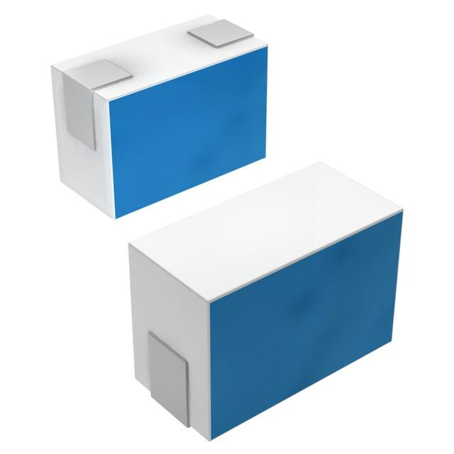
7. 封装信息:文档提供了电感的尺寸信息,包括标记、方向识别标记、单位质量等。
8. 电气性能测试条件:包括在特定温度和湿度下进行的测试。
9. 包装规格:包括胶带的尺寸、卷的规格、包装数量等。
10. 注意事项:文档最后提供了使用这些电感时的注意事项,包括限制应用、额定参数、浪涌电流、故障安全、使用前的评估等。