This series is not a recommended product.
Not recommended for new design.
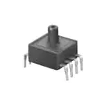
Pressure Sensor
PS-A (ADP5) series
(Built-in amplification and temperature compensating circuit)
Built-in amplifier and compensating circuit
Feature
● Built-in amplifier and temperature compensation circuit, no need for circuit design and characteristic adjustment.
● High accuracy and reliability : overall accuracy ±1.25% FS (Standard), ±2.5% FS (Low-pressure type)
● Compact size, space-saving : compatible size for PS type (Standard/Economy, S and M packages)
● RoHS compliant
Typical applications
● Industrial use :Pressure switches and pneumatic components, compressed air pressure measuring devices
● Medical use
:Airbeds
● Others
:Pressure sensing devices for air pressure mediums
[Low-pressure type]
● Water level detection for domestic appliances
:Washing machines and dishwashers
● Air pressure control
:Cleanrooms and smoking rooms
Ordering information
1
ADP5
Terminal profile
5
Code
Rated pressure
0
±100 kPa
1
2
−100 kPa
25 kPa
4
100 kPa
5
200 kPa
6
500 kPa
7
1000 kPa
1 : DIP terminal
2 : SMD terminal
B6
1
Code
Package/Pressure inlet hole
S package
0
length : 3 mm 0.118 inch, dia : 3 mm 0.118 inch
M package
1
length : 5 mm 0.197 inch, dia : 3 mm 0.118 inch
P package (Only low pressure type)
3
length : 15.6 mm 0.615 inch, dia : 5.45 mm 0.215 inch
6 kPa
(Low pressure type)
Note : Some part numbers may not be available depending on the combination.
Please refer to the Table of PRODUCT TYPES on the next page.
Product types
Standard packing : Carton : 100 pcs.; Case : 1,000 pcs.
Package
(Pressure inlet
hole length)
Pressure
Terminal
Part No.
Standard / Economy type
M package
(5 mm 0.118 inch)
Standard type
S package
(3 mm 0.118 inch)
DIP
terminal
SMD
terminal
DIP
terminal
SMD
terminal
Low pressure type
P package
(15.6 mm 0.614 inch)
DIP
terminal
Standard type (with glass base)
±100 kPa
ADP5100
ADP5200
ADP5101
ADP5201
ー
−100 kPa
ADP5110
ADP5210
ADP5111
ADP5211
ー
25 kPa
ADP5120
ー
ADP5121
ー
ー
100 kPa
ADP5140
ADP5240
ADP5141
ADP5241
ー
200 kPa
ADP5150
ADP5250
ADP5151
ADP5251
ー
500 kPa
ADP5160
ADP5260
ADP5161
ADP5261
ー
1000 kPa
ADP5170
ADP5270
ADP5171
ADP5271
ー
ー
ー
ADP51B63
Low pressure type
6 kPa
ー
ー
Design and specifications are each subject to change without notice. Ask factory for the current technical specifications before purchase and/or use.
Should a safety concern arise regarding this product, please be sure to contact us immediately.
21-Nov-23
�Pressure Sensor / PS-A (ADP5)
Rating
●Standard type
Item
Standard type (with glass base)
Type of pressure
Gauge pressure
Pressure medium
Air*1
Rated pressure (kPa)
±100
Max. applied pressure
-100
25
100
200
500
Twice of the rated pressure
Ambient temperature
−10 ℃ to +60 ℃ 14 ℉ to +140 ℉ (no freezing or condensation)
Storage temperature
−20 ℃ to +85 ℃ −4 ℉ to +185 ℉ (no freezing or condensation)
Drive voltage
5±0.25 V
Temperature compensation range
Offset voltage*2,3,5
Rated output voltage*2,3,5
1000
1.5 times the
rated pressure
0 ℃ to 50 ℃ 32 ℉ to 122 ℉
2.5±0.05
0.5±0.05 V
4.5±0.05
4.5±0.05 V
(+when +100kPa)
Overall accuracy
±1.25 %FS*3,4,5
Current consumption
Max. 10 mA*2,3
*1: Please consult us for pressure media other than dry air, nitrogen, oxygen, carbon dioxide.
*2: Indicates output when temperature is 25 ℃ 77 ℉.
*3: Indicates output when drive voltage is 5 V. Although output fluctuates due to fluctuations in the drive voltage, this is not included.
*4: Overall accuracy indicates the accuracy of the offset voltage and rated output voltage at a temperature compensation range of 0 to 50 ℃
32 to 122 ℉.
*5: Accuracy is the value at the time of our shipping. Please set Zero-point calibration function on your products in order to safely use if the
offset voltage is shifted.
●Low pressure type
Item
Economy type (without glass base)
Type of pressure
Gauge pressure
Pressure medium
Air*1
Rated pressure (kPa)
6
Max. applied pressure
Twice of the rated pressure
Ambient temperature
0 ℃ to +70 ℃ 32 ℉ to +158 ℉ (no freezing or condensation)
Storage temperature
−30 ℃ to +100 ℃ −22 ℉ to +212 ℉ (no freezing or condensation)
Drive voltage
5±0.25 V
Temperature compensation range
0 ℃ to 70 ℃ 32 ℉ to 158 ℉
Offset voltage
0.5 V (Typical)*2
Span voltage
4.0 V (Typical)*2
Overall accuracy
±2.5 %FS*2,3,4
Current consumption
Max. 10 mA
*1: Please consult us for pressure media other than dry air, nitrogen, oxygen, carbon dioxide.
*2: Indicates output when drive voltage is 5 V. Although output fluctuates due to fluctuations in the drive voltage, this is not included.
*3: Overall accuracy indicates the accuracy of the offset voltage and span voltage at temperatures between 0 to 70 °C 32 to 158 °F (FS=4V)
*4: The initial offset voltage error is not included in the overall accuracy.
Design and specifications are each subject to change without notice. Ask factory for the current technical specifications before purchase and/or use.
Should a safety concern arise regarding this product, please be sure to contact us immediately.
21-Nov-23
�Pressure Sensor / PS-A (ADP5)
Reference data
[Standard type]
1. -① Output voltage
1. -② Overall accuracy
(Offset voltage)
(Representative example : ADP5170)
Drive voltage:5 V
Temperature:0 to 50 ℃ 32 to 122 ℉
Applied pressure:0 kPa
1.25
1.25
1.00
1.00
4
0.75
0.75
0.50
0.50
3
2
1
0
500
Pressure (kPa)
0.25
0
-0.25
-0.50
1000
-1.00
25 77
50 122
1.25
1.00
Accuracy (%FS)
3
2
1
1.25
1.00
0.75
0.75
0.50
0.50
0.25
0.25
0
-0.25
-0.50
-1.25
50 122
(Representative example : ADP5100)
Drive voltage:5 V
Temperature:0 to 50 ℃ 32 to 122 ℉
Applied pressure:+100 kPa
0
-0.25
-0.50
-0.75
-1.00
-1.00
100
25 77
Temperature (℃ ℉)
2. -③ Overall accuracy
(Rated output voltage)
(Representative example : ADP5100)
Drive voltage:5 V
Temperature:0 to 50 ℃ 32 to 122 ℉
Applied pressure:0 kPa
-0.75
0
Pressure (kPa)
-1.25
0 32
2. -② Overall accuracy
(Offset voltage)
4
Output voltage (V)
0 32
Temperature (℃ ℉)
(Representative example : ADP5100)
Drive voltage:5 V
Temperature:25 ℃ 77 ℉
Applied pressure:-100 to +100 kPa
0
0
-100
-0.50
-0.75
2. -① Output voltage
5
0
-0.25
-1.00
-1.25
(Representative example : ADP5170)
Drive voltage:5 V
Temperature.:0 to 50 ℃ 32 to 122 ℉
Applied pressure:+1,000 kPa
0.25
-0.75
Accuracy (%FS)
0
Accuracy (%FS)
5
Accuracy (%FS)
Output voltage (V)
(Representative example : ADP5170)
Drive voltage:5 V
Temperature:25 ℃ 77 ℉
Applied pressure:0 to +1,000 kPa
1. -③ Overall accuracy
(Rated output voltage)
32
25 77
Temperature (℃ ℉)
50 122
-1.25
32
Design and specifications are each subject to change without notice. Ask factory for the current technical specifications before purchase and/or use.
Should a safety concern arise regarding this product, please be sure to contact us immediately.
25 77
Temperature (℃ ℉)
50 122
21-Nov-23
�Pressure Sensor / PS-A (ADP5)
Reference data
[Low pressure type]
1. Output voltage
2. THB (high temperature high humidity bias test)
(ADP51B63)
Within 85 ℃ 185 ℉ and 85% RH
5 V applied between No.2 (Vdd) and No.3 (GND)
Applied pressure:0 kPa
1.00
4.5
4
0.80
4.3
3
2
1
0
0
3.0
Applied pressure (kPa)
0.60
0.40
0.20
0.00
6.0
Span voltage (V)
5
Offset voltage (V)
Output voltage(V)
(ADP51B63)
Drive voltage:5 V
Temperature:25 ℃ 77 ℉
Applied pressure:0 to 6 kPa
intial
100 h
500 h
4.1
3.9
3.7
3.5
intial
100 h
500 h
3. Ambient temperature characteristics (ADP51B63)
1.00
4.5
0.80
4.3
Span voltage (V)
Offset voltage (V)
Ambient temperature:25 ℃ 77 ℉ → 0 ℃ 32 ℉→ 10 ℃ 50 ℉ → 60 ℃ 140 ℉ → 70 ℃ 158 ℉
0.60
0.40
0.20
0.00
25 77
0 32
10 50
60 140
4.1
3.9
3.7
3.5
70 158
25 77
0 32
Temperature (℃ ℉)
10 50
60 140
70 158
Temperature (℃ ℉)
4. Shock test
1.00
4.5
0.80
4.3
Span voltage (V)
Offset voltage (V)
(ADP51B63)
Shock applied(981 m/s2, 3 times in x, y and z directions)
Applied pressure:0 kPa
0.60
0.40
0.20
0.00
4.1
3.9
3.7
intial
3.5
after test
intial
after test
5. Vibration test
1.00
4.5
0.80
4.3
Span voltage (V)
Offset voltage (V)
(ADP51B63)
Vibration applied(10 to 55 Hz, amplitude : 1.5mm, x, y and z directions, 2 hrs each)
Applied pressure:0 kPa
0.60
0.40
0.20
0.00
intial
after test
4.1
3.9
3.7
3.5
intial
after test
Design and specifications are each subject to change without notice. Ask factory for the current technical specifications before purchase and/or use.
Should a safety concern arise regarding this product, please be sure to contact us immediately.
21-Nov-23
�Pressure Sensor / PS-A (ADP5)
Reference data
6. Temperature/humidity cycle test
(ADP51B63)
Exposed to 10 cycles in the temperature and humidity conditions given below.
Applied pressure:0 kPa
Temp.
1 cycle (24h)
65 ℃ 149 ℉
65 ℃ 149 ℉
25 ℃
77 ℉
Time
3h
2.5 h
2.5 h
3h
2.5 h 1.5 h
1.00
4.5
0.80
4.3
0.60
0.40
0.20
0.00
intial
3.5 h
25 ℃
77 ℉
3h
0 % RH
95 % RH
Span voltage (V)
Offset voltage (V)
□□□
2.5 h
-10 ℃
14 ℉
4.1
3.9
3.7
3.5
10 cyc
intial
10 cyc
Evaluation test
Classifi cation
Environmental
characteristics
Tested item
Tested condition
Storage at high
temperature
Temperature
Storage at low
temperature
Temperature
Humidity
Time
Time
Temperature/humidity
Time
Temperature
Temperature cycle
1 cycle
High temperature/
high humidity operation
Temperature/humidity
Times of cycle
Endurance
characteristics
Vibration resistance
Mechanical
characteristics
Applied vibration direction
Dropping height
Dropping resistance
Solderbility
:100 hrs
:Left in a –20 ℃ –4 ℉ constant temperature bath
:100 hrs
:Left at 40 ℃ 104 ℉, 90 % RH
:100 時間
Times
:30 min
Heat resistance (DIP)
Temperature
Time
Passed
Passed
Passed
Passed
:100 cycle
:40 ℃ 104 ℉, 90% RH
:106, rated voltage applied
:X, Y, Z 3 directions
Passed
Passed
:2 hrs each
:75 cm 29.528 inch
:2 times
Pulling strength :9.8 N {1 kgf}, 10 sec
Bending strength :4.9 N {0.5 kgf}, left and right 90 ° 1 time
Temperature
:230 ℃ 446 ℉
Time
Result
:–20 ℃ to 85 ℃ –4 ℉ to 185 ℉
Double amplitude :1.5 mm 0.059 inch
Vibration
:10 to 55 Hz
Time
Terminal strength
Soldering
characteristics
Operation times
:Left in a 85 ℃ 185 ℉ constant temperature bath
:5 sec
:260 ℃ 500 ℉
:10 sec
Passed
Passed
Passed
Passed
Note: For details other than listed above, please consult us.
Items
Criteria
Offset valtage
Variation amount
Output span voltage
within ±2.5 %FS of value
Design and specifications are each subject to change without notice. Ask factory for the current technical specifications before purchase and/or use.
Should a safety concern arise regarding this product, please be sure to contact us immediately.
21-Nov-23
�Pressure Sensor / PS-A (ADP5)
Dimensions
The CAD data of the products with a
mark can be downloaded from: http://industrial.panasonic.com/
CAD data
● Standard type S package (Terminal direction : DIP terminal Pressure inlet hole length : 3 mm 0.118 inch) ADP51□0
CAD data
7.0 max.
0.276 max.
6-Φ0.9
6-Φ0.035
4-R0.7
4-R0.028
NC
Φ3.0 Φ0.118
C
R0.2 R0.08
GND
6.5
0.256
⑥ ⑤ ④
2.5
0.098
0.5
0.020
2.5
0.098
2.5
0.098
GND NC
Atmospheric
pressure inlet hole
2.5
0.098
9.5
0.374
NC
Name
Vcc (Power supply ⊕)
NC (No connection)
Vout (Output)
NC (No connection)
NC (No connection)
GND (Ground)
Terminal No.
1
2
3
4
5
6
7.2
0.283
JAPAN
Vcc
Vout
① ② ③
1.8
0.071
3.0
0.118
GND NC
Vcc
(DC5V)
7.5
0.295
Φ2.2
Φ0.087
Terminal connection diagram
Recommended PC board
pattern (TOP VIEW)
NC Vout
7.2 max.
0.283 max.
Vcc
Pressure
inlet hole
NC Vout
7.0
0.276
Unit:mm inch, General tolerance ±0.3 ±0.012
Note: leave terminal "No connection" unconnected.
● Standard type S package (Terminal direction : SMD terminal Pressure inlet hole length : 3 mm 0.118 inch) ADP52□0
CAD data
Recommended PC board
pattern(TOP VIEW)
NC Vout
1.9
0.075
4-R0.7
4-R0.028
R0.2 R0.08
C
GND
⑥ ⑤ ④
0.15
0.059
6.5
0.256
0.5
0.020
2.5
0.098
2.5
0.098
GND NC
0.5
0.020
2.5
0.098
2.5
0.098
10.0
0.394
NC
Terminal No.
Vcc
1
2
3
4
5
6
7.2
0.283
Atmospheric
pressure inlet hole
JAPAN
NC Vout
7.0
0.283
Vout
① ② ③
1.1 0.043
9.5
0.374
GND NC NC
Φ3.0 Φ0.118
Vcc
(DC5V)
1.8
0.071
3.0
0.118
7.0 max.
0.276 max.
Φ2.2
Φ0.087
7.2 max.
0.283 max.
Vcc
Pressure
inlet hole
Terminal connection diagram
Unit:mm inch, General tolerance ±0.3 ±0.012
Name
Vcc (Power supply ⊕)
NC (No connection)
Vout (Output)
NC (No connection)
NC (No connection)
GND (Ground)
Note: leave terminal "No connection" unconnected.
Design and specifications are each subject to change without notice. Ask factory for the current technical specifications before purchase and/or use.
Should a safety concern arise regarding this product, please be sure to contact us immediately.
21-Nov-23
�Pressure Sensor / PS-A (ADP5)
Dimensions
CAD data
The CAD data of the products with a
mark can be downloaded from: http://industrial.panasonic.com/
● Standard/Economy type M package (Terminal direction : DIP terminal Pressure inlet hole length : 5 mm 0.197 inch) ADP51□1
ADP51□1/ADP51A11
CAD data
Recommended PC board
pattern(TOP VIEW)
NC Vout
7.0 max.
0.276 max.
Φ2.2
Φ0.087
5.0
0.197
GND NC
Terminal connection diagram
Vcc
(DC5V)
6-Φ0.9
6-Φ0.035
4-R0.7
4-R0.028
NC
Φ3.0 Φ0.118
Vout
① ② ③
C
7.5
0.295
Vcc
7.2 max.
0.283 max.
Pressure
inlet hole
R0.2 R0.08
GND
8.5
0.256
1.8
0.071
⑥ ⑤ ④
2.5
0.098
2.5
0.098
0.5
0.020
2.5
0.098
2.5
0.098
GND NC
Atmospheric
pressure inlet hole
9.5
0.374
NC
Name
Vcc (Power supply ⊕)
NC (No connection)
Vout (Output)
NC (No connection)
NC (No connection)
GND (Ground)
Terminal No.
7.2
0.283
JAPAN
Vcc
1
2
3
4
5
6
NC Vout
7.0
0.276
Unit:mm inch, General tolerance ±0.3 ±0.012
Note: leave terminal "No connection" unconnected.
● Standard/Economy type M package (Terminal direction : SMD terminal Pressure inlet hole length : 5 mm 0.197 inch) ADP52□1
CAD data
Recommended PC board
pattern(TOP VIEW)
NC Vout
GND NC NC
Φ3.0 Φ0.118
1.9
0.075
9.5
0.374
C
GND
⑥ ⑤ ④
0.15
0.059
8.5
0.256
GND NC
10.0
0.394
NC
2.5
0.098
2.5
0.098
0.5
0.020
Terminal No.
Vcc
1
2
3
4
5
6
7.2
0.283
JAPAN
NC Vout
7.0
0.276
Vout
① ② ③
1.1 0.043
4-R0.7
4-R0.028
R0.2 R0.08
0.5
0.020
2.5
0.098
2.5
0.098
Atmospheric
pressure inlet hole
Vcc
(DC5V)
1.8
0.071
5.0
0.197
7.0 max.
0.276 max.
Φ2.2
Φ0.087
7.2 max.
0.283 max.
Vcc
Pressure
inlet hole
Terminal connection diagram
Unit:mm inch, General tolerance ±0.3 ±0.012
Name
Vcc (Power supply ⊕)
NC (No connection)
Vout (Output)
NC (No connection)
NC (No connection)
GND (Ground)
Note: leave terminal "No connection" unconnected.
Design and specifications are each subject to change without notice. Ask factory for the current technical specifications before purchase and/or use.
Should a safety concern arise regarding this product, please be sure to contact us immediately.
21-Nov-23
�Pressure Sensor / PS-A (ADP5)
Dimensions
CAD data
The CAD data of the products with a
mark can be downloaded from: http://industrial.panasonic.com/
● Low pressure type P package (Terminal direction : DIP terminal, Pressure inlet hole length : 15.6 mm 0.614 inch) ADP51B63
P2.54x3=7.62 P0.100 x 3=0.300
Pressure
inlet hole
2.54
0.100
10.4
0.409
Atmospheric
pressure inlet hole
Recommended PC board
pattern(BOTTOM VIEW)
10.4 0.409
①②③④
0.01 μF
1.0 μF
2.54
0.100
0.25
0.010
3.3
0.130
8-Φ1.2
8-Φ0.047
15.6
0.614
Φ3.0
Φ0.118
Φ5.45 Φ0.215
⑧⑦⑥⑤
P2.54x3=7.62 P0.100x3=0.300
5.6
0.220
20.2
0.795
14.0 0.551
Terminal connection
diagram
13.97
0.550
CAD data
Unit:mm inch, General tolerance ±0.3 ±0.012
0.76
0.030
NC Vcc GNG Vout
NC NC NC NC
Terminal No.
Name
Terminal No.
Name
1
NC (No connection)
5
NC (No connection)
2
Vcc (Power supply⊕)
6
NC (No connection)
3
GND (Ground)
7
NC (No connection)
4
Vout (Output)
8
NC (No connection)
Note: leave terminal "No connection" unconnected.
Design and specifications are each subject to change without notice. Ask factory for the current technical specifications before purchase and/or use.
Should a safety concern arise regarding this product, please be sure to contact us immediately.
21-Nov-23
�Glossary of Common Terms for Pressure Sensors
Explanation of terms
■ Pressure object
This is what can be used to activate the pressure sensor.
(The Panasonic Corporation pressure sensor can beused with gas.)
■ Rated pressure
The pressure value up to which the specifications of the pressure sensor are guaranteed.
■ Maximum applied pressure
The maximum pressure that can be applied to the pressure sensor, after which, when the pressure is returned
to below the rated pressure range, the specifications of the pressure sensor are guaranteed.
■ Temperature compensation range
The temperature range across which the specification values of the pressure sensor are guaranteed.
■ Drive current (voltage)
The supply current (voltage) required to drive a pressure sensor.
■ Output span voltage
The difference between the rated output voltage and the offset voltage. The output span voltage is also called
the full-scale voltage (FS).
■ Offset voltage
The output voltage of a pressure sensor when no pressure is applied.
■ Rated pressure output voltage
Output voltage when rated pressure is applied.
■ Linearity
When the pressure is varied from no load to the rated pressure, the linearity is the amount of shift between
the straight line that joins the no-load voltage value and the rated pressure voltage value (expressed as the
ratio of the amount of shift (D1) at half of the rated pressure value with respect to the full scale voltage (FS)).
■ Output hysteresis
D1
FS
D2
Offset
voltage
No load
1/2 rated pressure
Rated pressure output voltage
Output voltage
The ratio of the difference (D2) in the noload output voltages when the pressure is varied from no load to
the rated pressure then reduced back to no load, with respect to the full scale voltage (FS).
Rated pressure
■ Offset voltage temperature characteristic
The variation of the offset voltage with changes in ambient temperature. The difference between the offset
voltage at the standard temperature and the offset values at the compensation lower limit temperature
(low temperature) (D1) and compensation upper limit temperature (high temperature) (D2) are obtained,
and the offset voltage temperature characteristic is expressed as the ratio of the larger of these two
differences (absolute) with respect to the full scale voltage (FS).
Design and specifications are each subject to change without notice. Ask factory for the current technical specifications before purchase and/or use.
Should a safety concern arise regarding this product, please be sure to contact us immediately.
31-Mar-20
�Glossary of Common Terms for Pressure Sensors
Explanation of terms
■ Temperature sensitivity characteristic
Output voltage
The variation of the sensitivity with changes in ambient temperature (variation in full scale (FS)).
The difference between the full scale voltage at the standard temperature (FS) and the full scale values at the
compensation lower limit temperature (low temperature) (FS1) and compensation upper limit temperature
(high temperature) (FS2) are obtained, and the offset voltage temperature characteristic is expressed as the ratio
of the larger of these two differences (FS1 - FS and FS2 - FS (absolute)) with respect to the full scale voltage (FS).
Compensation upper limit temperature
FS3
Δ2
Standard temperature
FS2
FS1
Δ1
No load
Compensation lower limit temperature
Rated pressure
■ Bridge resistance
Refers to the resistance value of a piezo resistance formed on a monolithic silicon substrate.
For example, the values of the resistances R1 to R4 in the bridge are typically 5 kΩ each.
✽ When the resistances of the resistive elements R1 to R4 that comprise the bridge are 5 kΩ each, the
equivalent composite resistance of the bridge is 5kΩ (3 kΩ bridges are also available).
R2
R1
R3
R4
The bridge resistance is the
resistance of the four resistive
elements that make up the bridge
expressed as one combined resistance.
■ Overall accuracy
Accuracy of offset voltage and rated pressure output voltage within the temperature compensation range.
Design and specifications are each subject to change without notice. Ask factory for the current technical specifications before purchase and/or use.
Should a safety concern arise regarding this product, please be sure to contact us immediately.
31-Mar-20
�Safety and Legal Matters to Be Observed
Safety and Legal Matters to Be Observed
Product specifications and applications
■ Please be advised that this product and product specifications are subject to change without notice for
improvement purposes. Therefore, please request and confirm the latest delivery specifications that explain
the specifications in detail before the final design, or purchase or use of the product, regardless of the
application. In addition, do not use this product in any way that deviates from the contents of the company's
delivery specifications.
■ Unless otherwise specified in this catalog or the product specifications, this product is intended for use in
general electronic equipment (AV products, home appliances, commercial equipment, office equipment,
information and communication equipment, etc.).
When this product is used for the following special cases, the specification document suited to each application
shall be signed/sealed (with Panasonic and the user) in advance..These include applications requiring special
quality and reliability, wherein their failures or malfunctions may directly threaten human life or cause harm to
the human body (e.g.: space/aircraft equipment, transportation/traffic equipment, combustion equipment,
medical equipment, disaster prevention/crime prevention equipment, safety equipment, etc.).
Safety design and product evaluation
■ Please ensure safety through protection circuits, redundant circuits, etc., in the customer's system design so
that a defect in our company's product will not endanger human life or cause other serious damage.
■ This catalog shows the quality and performance of individual parts. The durability of parts varies depending on
the usage environment and conditions. Therefore, please ensure to evaluate and confirm the state of each part
after it has been mounted in your product in the actual operating environment before use.
If you have any doubts about the safety of this product, then please notify us immediately, and be sure to conduct
a technical review including the above protection circuits and redundant circuits at your company.
Laws / Regulations / Intellectual property
■ The transportation of dangerous goods as designated by UN numbers, UN classifications, etc., does not apply
to this product. In addition, when exporting products, product specifications, and technical information described
in this catalog, please comply with the laws and regulations of the countries to which the products are exported,
especially those concerning security export control.
■ Each model of this product complies with the RoHS Directive (Restriction of the use of hazardous substances in
electrical and electronic equipment) (2011/65/EU and (EU) 2015/863). The date of compliance with the RoHS
Directive and REACH Regulation varies depending on the product model.
Further, if you are using product models in stock and are not sure whether or not they comply with the RoHS
Directive or REACH Regulation, please contact us by selecting "Sales Inquiry" from the inquiry form.
■ During the manufacturing process of this product and any of its components and materials to be used,
Panasonic does not intentionally use ozone-depleting substances stipulated in the Montreal Protocol and
specific bromine-based flame retardants such as PBBs (Poly-Brominated Biphenyls) / PBDEs (Poly-Brominated
Diphenyl Ethers). In addition, the materials used in this product are all listed as existing chemical substances
based on the Act on the Regulation of Manufacture and Evaluation of Chemical Substances.
■ With regard to the disposal of this product, please confirm the disposal method in each country and region
where it is incorporated into your company's product and used.
■ The technical information contained in this catalog is intended to show only typical operation and application
circuit examples of this product. This catalog does not guarantee that such information does not infringe upon
the intellectual property rights of Panasonic or any third party, nor imply that the license of such rights has been
granted.
Panasonic Industry will assume no liability whatsoever if the use of our company's
products deviates from the contents of this catalog or does not comply with the
precautions. Please be advised of these restrictions.
01-Dec-23
�Matters to Be Observed When Using This Product
Matters to Be Observed When Using This Product
(Pressure sensor / PS-A)
Use environments and cleaning conditions
■ Do not use or store the sensor with a non-air medium, especially in a medium containing a corrosive gas (organic solvent,
sulfur dioxide, hydrogen sulfide, etc.), moisture, foreign matter, or the like. Do not use the sensor with a harmful medium,
such as a corrosive gas, a combustible gas, or a toxic gas. There is a possibility that a tiny amount of the harmful medium
will leak out and exert a harmful effect on the surrounding environment and the human body.
■ The sensor does not have a waterproof structure. Avoid using the sensor in a place where water, etc., may splash on the
sensor or an environment where dew concentrates on the sensor. When water on the sensor freezes, it may lead to a
change in the output from the sensor or even the destruction of the sensor.
■ Because of the structural features of the sensor, the sensor output fluctuates when the sensor is exposed to light.
Avoid the sensor being exposed to light, etc., especially, when pressure is applied to the sensor through a transparent
tube.
■ Do not use the sensor in a situation where high-frequency vibrations, such as ultrasonic waves, are applied to the sensor.
■ The sensor may malfunction when exposed to static electricity, lightening, or electric noise from a cellular phone, radio
transmitter, broadcasting station, etc.
■ Since the sensor is open to the ambient air, be careful not to let cleaning solution flow into the sensor. Do not clean the
sensor by using ultrasonic waves. It may cause the sensor to fail.
Handling conditions
■ Use the sensor in the rated voltage range. Applying voltage outside the rated voltage range to the sensor can cause an
accident or breakage of the sensor. Select the way the sensor, lead-in tube, etc., are fixed in accordance with the pressure
being applied to the sensor. If you have any question, please feel free to contact us.
■ The sensor has a built-in sensor chip located close to the pressure lead-in port. Inserting a foreign object, such as a
needle, in the pressure lead-in port damages the chip or blocks up the lead-in port. Never do this. Do not block up the
pressure lead-in port.
■ When coating the board carrying the sensor with a potting agent, etc., make sure that the potting agent does not go into
the pressure lead-in port and the ambient pressure lead-in port. Thermal expansion/shrinkage of a resin coating the
sensor applies stress to the sensor. Use a resin with elasticity as a sealing agent (potting agent) after sufficiently
evaluating its properties.
■ The sensor may be destroyed by static electricity. Keep the sensor in a storage condition in which its terminals are
short-circuited via a conductive material or the whole sensor is wrapped with aluminum foil, etc. Because a plastic
container becomes charged with static electricity easily, avoid using a plastic container for storage or transportation
of the sensor. When using the sensor, let surrounding objects release static electricity safely by grounding the operator,
charged objects on the table, etc.
Circuit design and circuit board design
■ Connect the sensor in accordance with the terminal connection diagram. Do not connect the sensor in reverse polarity
to the power supply or connect a free terminal. Such wiring will lead to breakage or deterioration of the sensor.
■ To ensure the sensor’s resistance to noise superposed on source voltage, make sure to provide the power input
terminals of the sensor with capacitors to stabilize the source voltage. We recommend to dispose a 0.1 μF capacitor
and a 1,000 pF capacitor in parallel with each other. Make sure to select or add an optimum capacitor after confirming
the sensor’s resistance to noise in the actual circuit configuration where the sensor is provided with the capacitor.
■ An external surge voltage applied to the sensor damages its internal circuit. Use a surge absorber to protect the sensor
from incoming surges.
■ Adopt a printed board with a land wide enough to affix the sensor thereon.
30-Jun-23
�Matters to Be Observed When Using This Product
Mounting conditions
■ A sensor has a small structure with a small heat capacity. When soldering the sensor, keep the effects of external heat
on the sensor as small as possible. A sensor exposed to intensive heat thermally deforms, which may lead to breakage
or change in characteristics.
■ Use non-corrosive, rosin-based solder flux. The sensor is structured to be open to the ambient air. Make sure that solder
flux does not flow into the sensor.
■ Perform manual soldering in the following manner: clean the soldering iron tip sufficiently and then finish soldering,
with the soldering iron tip heated to 260 ℃ to 300 ℃ (30 W), within 5 seconds. Do not apply a load to the sensor terminals.
It may change the output from the sensor.
■ Perform flow soldering (DIP terminal type) with a flow soldering tank temperature kept at 260 ℃ or lower and within
5 seconds. When the sensor is mounted on a board with a small heat capacity, the sensor may thermally deform when
exposed to soldering heat. In this case, avoid flow soldering.
■ In the case of reflow soldering (SMD terminal type), we recommend solder-paste screen printing as a solder paste
printing method.
■ For a footprint pattern on the printed board, refer to the printed board recommended specification diagram. Because
self-alignment of solder is insufficient in some cases, carefully align the terminals of the sensor and the pattern.
■ The recommended reflow temperature profile is shown below. The temperature measurement shown in the
temperature profile is the value measured at a part of board that is close to the terminals.
Main heating
Temperature
230°C
220°C
Preheating
150°C
60 seconds or less
10 seconds
or
less
Time
■ The front end of the pressure lead-in port may melt or deform under high temperature, depending on the equipment
or conditions. Make sure to conduct a confirmation test under the actual mounting conditions.
■ Complete rework on a soldered part in a single process. When reworking a solder bridge, use a solder iron with a
flat tip and do not apply any additional solder flux. Use a solder iron with a tip temperature equal to or lower than the
tip temperature specified in the specification sheet.
■ A warped printed board applies stress to the sensor, which may change the characteristics of the sensor. Conduct
a characteristics confirmation test after the soldering process. When cutting or folding the board after mounting the
sensor on the board, be careful that no stress is applied to the soldered area.
■ The sensor has external terminals exposed from its body. A metal piece, etc., coming in contact with the exposed
terminals, causes problems with output from the terminals. Prevent metal pieces, bare hands, etc., from coming in
contact with the terminals. Excessive force applied to the terminals deforms the terminals, thus impairing the
solderability of the sensor. Do not drop the sensor, and do not handle it roughly, either.
■ When coating the board to prevent the deterioration of insulation properties after the soldering process, make sure
that no chemical sticks to the sensor.
30-Jun-23
�


 工商网监
湘ICP备2023018690号
工商网监
湘ICP备2023018690号
