DATA SHEET
LDMOS FIELD EFFECT TRANSISTOR
NE55410GR
N-CHANNEL SILICON POWER LDMOS FET FOR 2 W + 10 W VHF to L-BAND SINGLE-END POWER AMPLIFIER
DESCRIPTION
The NE55410GR is an N-channel enhancement-mode LDMOS FET designed for driver 0.1 to 2.6 GHz PA, such as, cellular base station amplifier, analog/digital TV-transmitters, and the other PA’s. This product has two different FET's on one die manufactured using our NEWMOS technology (our WSi gate lateral MOS FET), and its nitride surface passivation and quadruple layer aluminum silicon metalization offer a high degree of reliability.
FEATURES
• Two different FET’s (Q1 : Pout = 2 W, Q2 : Pout = 10 W) in one package • Over 25 dB gain available by connecting two FET’s in series : GL (Q1) = 13.5 dB TYP. (VDS = 28 V, IDset (Q1) = 20 mA, f = 2 140 MHz) : GL (Q2) = 11.0 dB TYP. (VDS = 28 V, IDset (Q2) = 100 mA, f = 2 140 MHz) • High 1 dB compression output power : PO (1 dB) (Q1) = 35.4 dBm TYP. (VDS = 28 V, IDset (Q1) = 20 mA, f = 2 140 MHz) : PO (1 dB) (Q2) = 40.4 dBm TYP. (VDS = 28 V, IDset (Q2) = 100 mA, f = 2 140 MHz) • High drain efficiency • Low intermodulation distortion • Single Supply (VDS : 3 V < VDS ≤ 32 V) • Excellent Thermal Stability • Surface mount type and Super low cost plastic package : 16-pin plastic HTSSOP • Integrated ESD protection • Excellent stability against HCI (Hot Carrier Injection) : ηd (Q1) = 52% TYP. (VDS = 28 V, IDset (Q1) = 20 mA, f = 2 140 MHz) : ηd (Q2) = 46% TYP. (VDS = 28 V, IDset (Q2) = 100 mA, f = 2 140 MHz) : IM3 (Q1) = −40 dBc TYP. (VDS = 28 V, IDset (Q1+Q2) = 120 mA, f = 2 132.5/2 147.5 MHz, Pout = 33 dBm (2 tones) )
APPLICATION
• Digital cellular base station PA : W-CDMA/GSM/D-AMPS/N-CDMA/PCS etc. • UHF-band TV transmitter PA
Caution Observe precautions when handling because these devices are sensitive to electrostatic discharge.
The information in this document is subject to change without notice. Before using this document, please confirm that this is the latest version.
Not all products and/or types are available in every country. Please check with an NEC Electronics sales representative for availability and additional information.
Document No. PU10542EJ03V0DS (3rd edition) Date Published January 2007 NS CP(N) Printed in Japan
2004, 2007
The mark shows major revised points.
The revised points can be easily searched by copying an "" in the PDF file and specifying it in the "Find what:" field.
�NE55410GR
ORDERING INFORMATION
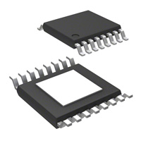
Part Number NE55410GR Order Number NE55410GR-T3-AZ Package 16-pin plastic HTSSOP (Pb-Free)
Note
Marking 55410
Supplying Form • Embossed tape 12 mm wide • Pin 1 and 8 indicates pull-out direction of tape • Qty 1 kpcs/reel
Note With regards to terminal solder (the solder contains lead) plated products (conventionally plated), contact your nearby sales office. Remark To order evaluation samples, contact your nearby sales office. Part number for sample order: NE55410GR
PIN CONNECTIONS AND INTERNAL BLOCK DIAGRAM
(Top View) S 9 10 11 12 13 14 15 16 S S S S Q2 S S S S Q1 S 8 7 6 5 4 3 2 1
6 7 8 Source Gate (Q1) Source 14 15 16 Gate (Q2) Gate (Q2) Source Pin No. 1 2 3 4 5 Pin Name Source Drain (Q2) Drain (Q2) Drain (Q2) Drain (Q2) Pin No. 9 10 11 12 13 Pin Name Source Gate (Q1) Source Drain (Q1) Source
S
Remark All the terminals of a Q2 connected to a circuit. Backside : Source (S)
ABSOLUTE MAXIMUM RATINGS (TA = +25°C, unless otherwise specified)
Parameter Drain to Source Voltage Gate to Source Voltage Drain Current (Q1) Drain Current (Q2) Total Device Dissipation (Tcase = 25°C) Input Power (Q1) Input Power (Q2) Channel Temperature Storage Temperature Symbol VDS VGS ID (Q1) ID (Q2) Ptot Pin (Q1) Pin (Q2) Tch Tstg f = 2.14 GHz, VDS = 28 V f = 2.14 GHz, VDS = 28 V Test Conditions Ratings 65 ±7 0.25 1.0 40 0.3 1.5 150 −65 to +150 Unit V V A A W W W °C °C
2
Data Sheet PU10542EJ03V0DS
�NE55410GR
THERMAL RESISTANCE (TA = +25°C)
Parameter Channel to Case Resistance Symbol Rth (ch-c) Test Conditions MIN. − TYP. 2.5 MAX. 3.0 Unit °C/W
RECOMMENDED OPERATING CONDITIONS (TA = +25°C)
Parameter Symbol VDS VGS Pin (Q1) Pin (Q2)
Note
MIN. − 2.7 − − − −
TYP. 28 3.3 15 20 − −
MAX. 32 3.7 23 30 24 30
Unit V V dBm dBm dBm dBm
Drain to Source Voltage Gate to Source Voltage Input Power (Q1), CW Input Power (Q2), CW
Average Output Power (Q1), CW Average Output Power (Q2), CW
PO (ave.) (Q1) PO (ave.) (Q2)
Note
Note When mounting on the PWB that our company recommends.
ELECTRICAL CHARACTERISTICS (TA = +25°C)
Parameter Q1 Gate to Source Leak Current Drain to Source Leakage Current Gate Threshold Voltage Transconductance Drain to Source Breakdown Voltage Q2 Gate to Source Leak Current Drain to Source Leakage Current Gate Threshold Voltage Transconductance Drain to Source Breakdown Voltage IGSS (Q2) IDSS (Q2) Vth (Q2) gm (Q2) VGSS = 5V VDSS = 65 V VDS = 10 V, IDS = 1 mA VDS = 28 V, IDS = 100 mA − − 2.0 − 65 − − 2.6 0.45 75 1 1 3.2 − − IGSS (Q1) IDSS (Q1) Vth (Q1) gm (Q1) VGSS = 5V VDSS = 65 V VDS = 10 V, IDS = 1 mA VDS = 28 V, IDS = 20 mA − − 2.2 − 65 − − 2.8 0.09 75 1 1 3.4 − − Symbol Test Conditions MIN. TYP. MAX. Unit
μA
mA V S V
BVDSS (Q1) IDSS = 10 μA
μA
mA V S V
BVDSS (Q2) IDSS = 10 μA
Data Sheet PU10542EJ03V0DS
3
�NE55410GR
RF CHARACTERISTICS (TA = +25°C)
Parameter Q1 Gain 1 dB Compression Output Power Drain Efficiency Linear Gain Q2 Gain 1 dB Compression Output Power Drain Efficiency Linear Gain Gain 1 dB Compression Output Power Drain Efficiency Linear Gain Q1 + Q2 Gain 1 dB Compression Output Power Drain Efficiency Linear Gain Gain 1 dB Compression Output Power Drain Efficiency Output Power Linear Gain 3rd Order Intermodulation Distortion Drain Efficiency PO (1 dB) f = 880 MHz, VDS = 28 V, IDset = 120 mA (Q1 + Q2) − − − f = 2 140 MHz, VDS = 28 V, IDset = 120 mA (Q1 + Q2) − 34 39 24 f = 2 132.5/2 147.5 MHz, VDS = 28 V, 2 carrier W-CDMA 3GPP, Test Model1, 64DPCH, 67% Clipping, IDset = 120 mA (Q1 + Q2), Ave Pout = 33 dBm − − 41.5 55 30 40.0 42 40 25 −40 21 − − − − − − − − − dBm % dB dBm % dB dB dBc % PO (1 dB) f = 2 140 MHz, VDS = 28 V, IDset = 100 mA − − 9.5 f = 1 840 MHz, VDS = 28 V, IDset = 100 mA − − − 40.4 46 11 40.5 49 14 − − − − − − dBm % dB dBm % dB PO (1 dB) f = 2 140 MHz, VDS = 28 V, IDset = 20 mA − − 12 35.4 52 13.5 − − − dBm % dB Symbol Test Conditions MIN. TYP. MAX. Unit
ηd
GL
Note1
ηd
GL
Note2
PO (1 dB)
ηd
GL
Note2
ηd
GL
Note3
PO (1 dB)
ηd
Pout GL
Note4
IM3
ηd
Notes 1. Pin = 15 dBm 2. Pin = 20 dBm 3. Pin = 5 dBm 4. Pin = 10 dBm
4
Data Sheet PU10542EJ03V0DS
�NE55410GR
TYPICAL CHARACTERISTICS (TA = +25°C, VDS = 28 V, IDset = 120 mA, unless otherwise specified)
3rd/5th Order Intermodulation Distortion IM3/IM5 (dBc)
GAIN, DRAIN EFFICIENCY, vs. OUTPUT POWER
36 34 32
Gain G (dB)
IM3/IM5 vs. 2 TONES OUTPUT POWER
–10
Lower Upper
Drain Efficiency ηd (%)
f = 840 MHz 860 MHz 880 MHz 900 MHz 920 MHz G
80 70 60 50 40
–20 IM3 –30 –40 –50 –60 –70 15
CW, f = 960 MHz, 1 MHz Spacing
30 28 26 24 22 20 20 25 30 35 40
ηd
30 20 10 0 45
IM5
20
25
30
35
40
45
Output Power Pout (dBm)
2 tones Output Power Pout (dBm)
GAIN, DRAIN EFFICIENCY, vs. OUTPUT POWER
30 28 26
Gain G (dB)
80 70 60 G 50 40
Drain Efficiency ηd (%)
24 22 20 18 16 14 20 25 30
ηd
f = 2.09 GHz 2.11 GHz 2.14 GHz 2.17 GHz 2.19 GHz 35 40
30 20 10 0 45
Output Power Pout (dBm)
3rd/5th Order Intermodulation Distortion IM3/IM5 (dBc)
IM3/IM5, DRAIN EFFICIENCY, vs. 2 TONES OUTPUT POWER
–20 –25 –30 –35 –40 –45 –50 –55 –60 –65 –70 15 20 25 30 35 40
Lower Upper
100 90 IM3 IM5
Drain Efficiency ηd (%)
80 70 60 50 40
W-CDMA 3GPP, Test Model 1, 64 DPCH, 67% Clipping, Center Frequency 2.14GHz, 15 MHz spacing
ηd
30 20 10 0 45
2 tones Output Power Pout (dBm)
Remark The graphs indicate nominal characteristics.
Data Sheet PU10542EJ03V0DS
5
�NE55410GR
S-PARAMETERS
S-parameters/Noise parameters are provided on our web site in a form (S2P) that enables direct import to a microwave circuit simulator without keyboard input. Click here to download S-parameters. [RF and Microwave] → [Device Parameters] URL http://www.ncsd.necel.com/microwave/index.html
6
Data Sheet PU10542EJ03V0DS
�NE55410GR
EVALUATION CIRCUIT (f = 840 to 960 MHz, VDS = 28 V, IDset = 120 mA)
VDS (+28 V) + B 6.8 kΩ 47μF
0.22 μF 1 kΩ
2.2 kΩ
NE55410GR TL5
0.001 μF
(open)7 RFin TL1 47 pF TL2 15 Ω TL3 10
Q1 12
TL4 47 pF
TL6
TL7
A
S 3 pF 14 Q2 2 3 4 5 TL12 TL13 6 pF 2 pF 2 pF TL14 TL15 TL16 TL17 TL18 RFout
TL8 A 15 pF 10 Ω 2.2 nH 56 nH
TL9
TL10
TL11
TL19
15 S
47 pF
9 pF
12 pF
4 pF
S SSSSSS S 1 6 8 9 11 13 16 (Back side) 0.22 μF
18 Ω 0.047 μF 1 kΩ
6.8 kΩ
B
Symbol TL1 TL2 TL3 TL4 TL5 TL6 TL7 TL8 TL9 TL10
Width (mm) Length (mm) 1.0 4.5 0.5 0.5 1.0 1.0 1.0 1.0 1.0 1.0 3.0 10.0 16.0 5.0 48.0 4.0 3.0 6.0 3.0 4.0
Symbol TL11 TL12 TL13 TL14 TL15 TL16 TL17 TL18 TL19
Width (mm) Length (mm) 1.0 1.0 0.8 1.0 1.0 1.0 1.0 1.0 1.0 3.0 5.0 48.0 6.5 10.5 9.5 10.0 6.0 3.0
The application circuits and their parameters are for reference only and are not intended for use in actual design-ins.
Data Sheet PU10542EJ03V0DS
7
�NE55410GR
EVALUATION CIRCUIT (f = 840 to 960 MHz, VDS = 28 V, IDset = 120 mA)
VGS (Q1), +28 V 6.8 kΩ 0.22 μF 2.2 kΩ 15 Ω 47 μF VDS (Q2), +28 V
1 kΩ (Valiable) RF in 0.22 μF
47 pF 6 pF 47 pF 2 pF
12 pF 3 pF
55410
4 pF
2 pF 2.2 nH 15 pF 1.5 pF 47 pF RF out
0.001 μF
18 Ω
10 Ω
56 nH
1 kΩ (Valiable)
6.8 kΩ
0.047 μ F
9 pF
VDS (Q1), +28 V
VGS (Q2), +28 V
8
Data Sheet PU10542EJ03V0DS
�NE55410GR
EVALUATION CIRCUIT (f = 2 090 to 2 190 MHz, VDS = 28 V, IDset = 120 mA)
VDS (+28 V) + B 6.8 kΩ 22 μF
0.22 μF 1 kΩ
TL3
NE55410GR TL8
0.22 μF
10 Ω RFin TL1 47 pF 8.5 pF TL12 0.75 pF 10 Ω 12 nH TL14 1 pF 2 pF TL2 TL4 TL5
7 (open) TL6 10
Q1 12
TL7 33 pF
TL9
TL10
TL11
A
S 1 pF 14 15 S Q2 2 3 4 5 TL15 TL17 TL18 TL19 TL20 TL21 RFout
A
TL13
15 pF TL16 3 pF 1 pF
S SSSSSS S 1 6 8 9 11 13 16 (Back side) 0.22 μF
10 Ω
0.22 μF 1 kΩ
6.8 kΩ
B
Symbol TL1 TL2 TL3 TL4 TL5 TL6 TL7 TL8 TL9 TL10 TL11
Width (mm) Length (mm) 1.0 1.0 1.0 1.0 1.0 0.5 0.5 1.0 1.0 4.5 1.0 17.0 4.0 24.5 2.5 3.0 2.5 4.5 25.5 2.5 4.5 3.5
Symbol TL12 TL13 TL14 TL15 TL16 TL17 TL18 TL19 TL20 TL21
Width (mm) Length (mm) 1.0 1.0 1.0 2.5 1.0 1.0 5.0 5.0 1.0 1.0 4.0 4.5 25.0 2.5 27.0 2.0 4.0 2.0 12.5 5.5
The application circuits and their parameters are for reference only and are not intended for use in actual design-ins.
Data Sheet PU10542EJ03V0DS
9
�NE55410GR
EVALUATION CIRCUIT (f = 2 090 to 2 190 MHz, VDS = 28 V, IDset = 120 mA)
VGS (Q1), +28 V 1 kΩ (Potentiometer) 0.22 μF 10 Ω VDS (Q2), +28 V 22 μF
6.8 kΩ
0.22 μF RF in 15 pF 0.5 pF 2 pF 33 pF
55410
3 pF 1 pF
1.0 pF
0.22 μF 12 nH 10 Ω
RF out
15 pF 0.75 pF 10 Ω 1 pF 0.22 μF 6.8 kΩ 1 kΩ (Potentiometer) VGS (Q2), +28 V
VDS (Q1), +28 V
10
Data Sheet PU10542EJ03V0DS
�NE55410GR
PACKAGE DIMENSIONS 16-PIN PLASTIC HTSSOP (UNIT: mm)
6.4±0.3 0.20±0.10 (1.8)
0.65±0.1
(0.4)
9
8
55410
NEC
0.20±0.10
5.5±0.3
16
1 (0.1) 5.2±0.2 0.9±0.2 (2.5)
(1.5)
Remark ( ): Reference value
LAND PATTERN (UNIT: mm)
6.40 5.20 0.10
0.50
0.28
0.24
0.28
0.20
0.65
0.40
0.50
0.28
1.15
0.24
0.50
1.50 4.00 0.48
Remarks1. Via holes : 158 holes 2. Hole size : φ 0.15 mm 3. Min. spacing : 0.354 mm 4. : Solder resist or etching
1.00
0.20
1.50
5.50
(2.7)
(0.5)
Data Sheet PU10542EJ03V0DS
11
�NE55410GR
RECOMMENDED SOLDERING CONDITIONS
This product should be soldered and mounted under the following recommended conditions. methods and conditions other than those recommended below, contact your nearby sales office.
Soldering Method Infrared Reflow Soldering Conditions Peak temperature (package surface temperature) Time at peak temperature Time at temperature of 220°C or higher Preheating time at 120 to 180°C Maximum number of reflow processes Maximum chlorine content of rosin flux (% mass) Wave Soldering Peak temperature (molten solder temperature) Time at peak temperature Maximum number of flow processes Maximum chlorine content of rosin flux (% mass) Partial Heating Peak temperature (terminal temperature) Soldering time (per side of device) Maximum chlorine content of rosin flux (% mass) : 260°C or below : 10 seconds or less : 60 seconds or less : 120±30 seconds : 3 times : 0.2%(Wt.) or below : 260°C or below : 10 seconds or less : 1 time : 0.2%(Wt.) or below : 350°C or below : 3 seconds or less : 0.2%(Wt.) or below HS350 WS260 Condition Symbol IR260
For soldering
Preheating temperature (package surface temperature) : 120°C or below
Caution Do not use different soldering methods together (except for partial heating).
12
Data Sheet PU10542EJ03V0DS
�NE55410GR
• T he information in this document is current as of January, 2007. The information is subject to change without notice. For actual design-in, refer to the latest publications of NEC Electronics data sheets or data books, etc., for the most up-to-date specifications of NEC Electronics products. Not all products and/or types are available in every country. Please check with an NEC Electronics sales representative for availability and additional information. • No part of this document may be copied or reproduced in any form or by any means without the prior written consent of NEC Electronics. NEC Electronics assumes no responsibility for any errors that may appear in this document. • NEC Electronics does not assume any liability for infringement of patents, copyrights or other intellectual property rights of third parties by or arising from the use of NEC Electronics products listed in this document or any other liability arising from the use of such products. No license, express, implied or otherwise, is granted under any patents, copyrights or other intellectual property rights of NEC Electronics or others. • Descriptions of circuits, software and other related information in this document are provided for illustrative purposes in semiconductor product operation and application examples. The incorporation of these circuits, software and information in the design of a customer's equipment shall be done under the full responsibility of the customer. NEC Electronics assumes no responsibility for any losses incurred by customers or third parties arising from the use of these circuits, software and information. • While NEC Electronics endeavors to enhance the quality, reliability and safety of NEC Electronics products, customers agree and acknowledge that the possibility of defects thereof cannot be eliminated entirely. To minimize risks of damage to property or injury (including death) to persons arising from defects in NEC Electronics products, customers must incorporate sufficient safety measures in their design, such as redundancy, fire-containment and anti-failure features. • NEC Electronics products are classified into the following three quality grades: "Standard", "Special" and "Specific". The "Specific" quality grade applies only to NEC Electronics products developed based on a customerdesignated "quality assurance program" for a specific application. The recommended applications of an NEC Electronics product depend on its quality grade, as indicated below. Customers must check the quality grade of each NEC Electronics product before using it in a particular application. "Standard": Computers, office equipment, communications equipment, test and measurement equipment, audio and visual equipment, home electronic appliances, machine tools, personal electronic equipment and industrial robots. "Special": Transportation equipment (automobiles, trains, ships, etc.), traffic control systems, anti-disaster systems, anti-crime systems, safety equipment and medical equipment (not specifically designed for life support). "Specific": Aircraft, aerospace equipment, submersible repeaters, nuclear reactor control systems, life support systems and medical equipment for life support, etc. The quality grade of NEC Electronics products is "Standard" unless otherwise expressly specified in NEC Electronics data sheets or data books, etc. If customers wish to use NEC Electronics products in applications not intended by NEC Electronics, they must contact an NEC Electronics sales representative in advance to determine NEC Electronics' willingness to support a given application. (Note) (1) "NEC Electronics" as used in this statement means NEC Electronics Corporation and also includes its majority-owned subsidiaries. (2) "NEC Electronics products" means any product developed or manufactured by or for NEC Electronics (as defined above).
M8E 02. 11-1
�