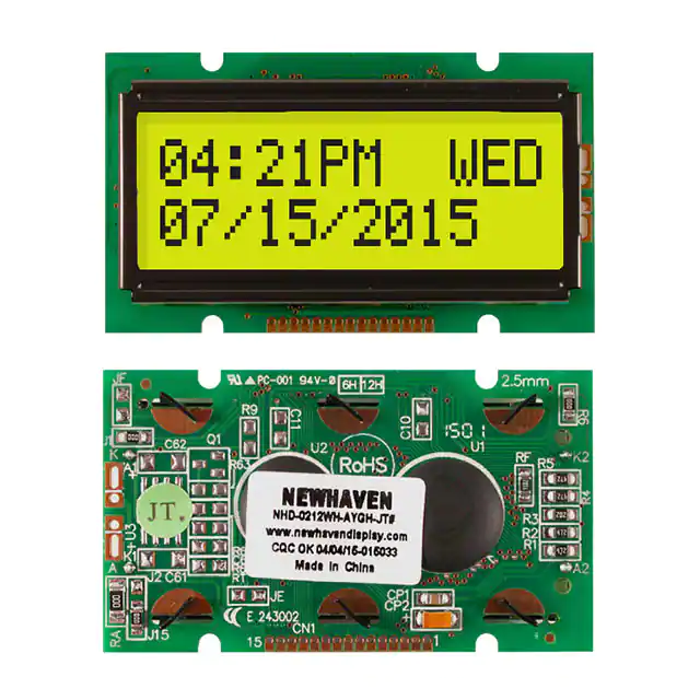
Product Specification
NHDCharacter Liquid Crystal Display Module
NHD -
Newhaven Display
Newhaven Display International, Inc.
2661 Galvin Court, Elgin, IL 60124 USA
Ph: 847.844.8795 | Fx: 847.844.8796
www.newhavendisplay.com
REACH
Compliant
RoHS
Compliant
�Table of Contents
Document Revision History ……………………………………………………………………………………………………………………..…. 2
Functions and Features …………………………………………………………………………………………………………………..………….. 2
Mechanical Drawing ………………………………………………………………………………………………………..…………….….……... 3
Pin Description and Wiring Diagram……….……………………………………………………………………………………….….……… 4
Driver Information ……………………………………………………………………………………………………..………………………………. 4
DDRAM Address …………………………………………………………………………………………………………………………………………. 4
Electrical Characteristics ……………………………………………………………………………….…………………………………….…….. 5
Optical Characteristics ………………………………………………………………………………………………………………………………… 5
Table of Commands ……………………………………………………………………………………………………………………………………. 6
Timing Characteristics ………………………………………………………………………………………………..………………………..….…. 7
Built-in Font Table …………………………………………………………………………………………………………….……………………….. 9
Example Initialization Program …………………………………………………………………………………………………………...……. 10
Quality Information ………………………………………………………………………………………………….…………….………………… 12
Additional Resources
➢ Support Forum: http://www.nhdforum.newhavendisplay.com
➢ Github: https://github.com/newhavendisplay
➢ Example Code: https://www.newhavendisplay.com/example_code.html
➢
Knowledge Center: https://www.newhavendisplay.com/knowledge_center.html
➢ Quality Center: https://www.newhavendisplay.com/quality_center.html
➢ Precautions for using LCDs/LCMs: https://www.newhavendisplay.com/specs/precautions.pdf
➢ Warranty / Terms & Conditions: https://www.newhavendisplay.com/terms.html
1
�Document Revision History
Revision
Date
Description
Changed By
0
9/20/2007
Initial Release
-
1
11/4/2009
User Guide Reformat
BE
2
1/5/2010
Optical revised
BE
3
1/6/2011
Alternate controller information updated
AK
4
4/10/2013
Mechanical drawing, Optical characteristics updated
AK
5
4/25/17
Mechanical Drawing and Electrical Characteristics Updated
TM
6
6/20/18
VLCD Updated
SB
7
3/24/20
Backlight Characteristics Updated
SB
8
4/29/21
Supply Voltage for LCD Contrast Updated
ZP
Functions and Features
•
•
•
•
•
2 lines x 12 characters
Built-in controller (ST7066U)
+5.0V Power Supply
1/16 duty, 1/5 bias
RoHS compliant
2
�1
A
2
3
Mechanical Drawing
4
5
6
7
SYMBOL
8
REVISION
DATE
A
3.20
2.65
0.55
0.45
10.15
8.75
7.25
3.65
0.5
51.3
4.5
4.85
46.7
46.0(VA)
8.93
37.85(AA)
9.7Max
5.1
1
2
3
4
5
6
7
8
9
10
11
12
13
14
15
30.0
11.7(AA)
17.5
14.5(VA)
24.7
32.0 0.5
C
D
1.0
18.96
17.78
12.25
E
F
Notes:
1. Driving:
2. Supply Voltage:
3. Display Type:
4. Op�mal View:
5. Backlight:
6. Driver IC:
1
1.5
4-R1.25
15- 0.7PTH
15- 1.0PAD
1.6
LED B/L
31.2
1/16 duty, 1/5 bias
5V VDD; 4.2 VLCD
STN Pos�ve / Gray / Transflec�ve
6:00
Yellow/Green LED
ST7066U 4-bit / 8-bit Parallel MPU Interface
2
3
4
B
6.20
5.50
0.70
0.60
2.2
1.0
55.7
B
C
Vss
Vdd
Vo
RS
R/W
E
DB0
DB1
DB2
DB3
DB4
DB5
DB6
DB7
A
D
E
Standard Tolerance:
(Unless otherwise specified)
Linear:
±0.3mm
Unless otherwise specified:
• Dimensions are in Millimeters
• Third Angle Projection
Revision:
Drawing/Part Number:
NHD-0212WH-AYGH-JT#
Drawn By:
Drawn Date:
K. Fraim
3/24/20
Approved By:
Approved Date:
Do Not Scale Drawing
1.0
Size:
A. Khan
3/24/20
A3
Scale:
X:X
Sheet 1 of 1
This drawing is solely the property of Newhaven Display International, Inc.
The information it contains is not to be disclosed, reproduced or copied in
whole or part without written approval from Newhaven Display.
5
6
7
8
F
�Pin Description and Wiring Diagram
Pin No.
Symbol
External Connection
1
2
3
4
5
6
7-10
VSS
VDD
V0
RS
R/W
E
DB0 – DB3
Power Supply
Power Supply
Adj Power Supply
MPU
MPU
MPU
MPU
11-14
15
DB4 – DB7
A
MPU
Power Supply
Function Description
Ground
Supply Voltage for logic (+5.0V)
Power supply for contrast (approx. 0.8V)
Register select signal. RS=0: Command, RS=1: Data
Read/Write select signal, R/W=1: Read; R/W: =0: Write
Operation enable signal. Falling edge triggered.
Four low order bi-directional three-state data bus lines.
These four are not used during 4-bit operation.
Four high order bi-directional three-state data bus lines.
Power supply for LED Backlight (+4.2V)
Recommended LCD connector: 1.27mm pitch pins
Backlight connector: --Mates with: ---
Controller Information
Built-in ST7066U controller.
Please download specification at http://www.newhavendisplay.com/app_notes/ST7066U.pdf
DDRAM Address
1 2 3 4 5 6 7 8 9 10 11 12
00 01 02 03 04 05 06 07 08 09 0A 0B
40 41 42 43 44 45 46 47 48 49 4A 4B
4
�Electrical Characteristics
Item
Operating Temperature Range
Storage Temperature Range
Supply Voltage
Supply Current
Supply for LCD (contrast)
“H” Level input
“L” Level input
“H” Level output
“L” Level output
Backlight Supply Voltage
Backlight Supply Current
Symbol
Condition
Min.
Typ.
Max.
Unit
TOP
TST
VDD
IDD
VDD – V0
VIH
VIL
VOH
VOL
Absolute Max
Absolute Max
TOP =25°C,
VDD=5.0V
-
-20
-30
4.5
0.5
4.1
0.7*VDD
VSS
3.9
-
5.0
1.0
4.2
-
+70
+80
5.5
2.0
4.3
VDD
0.6
VDD
0.4
⁰C
⁰C
V
mA
V
V
V
V
V
VLED
ILED
VLED = 4.2V
4.0
32
4.2
40
4.7
48
V
mA
Optical Characteristics:
Item
Viewing Angle – Top
Viewing Angle – Bottom
Viewing Angle – Left
Viewing Angle – Right
Contrast Ratio
Response Time (rise)
Response Time (fall)
Symbol
ϕY+
ϕYθXθX+
Cr
Tr
Tf
Condition
Cr ≥ 2
TOP =25°C
Min.
Typ.
Max.
Unit
-
20
40
30
30
3
150
150
200
200
⁰
⁰
⁰
⁰
ms
ms
5
�Table of Commands
Instruction code
Instruction
RS
R/W DB7 DB6 DB5 DB4 DB3 DB2 DB1 DB0
Clear
Display
0
0
0
0
0
0
0
0
0
Return
Home
0
0
0
0
0
0
0
0
1
Entry mode
Set
0
0
0
0
0
0
0
1
I/D
Display ON/
OFF control
0
0
0
0
0
0
1
D
C
Cursor or
Display shift
0
0
0
0
0
1
S/C
R/L
-
Function set
0
0
0
0
1
DL
N
F
-
0
0
0
1
0
0
1
Read busy
Flag and
Address
0
1
Write data
To Address
1
Read data
From RAM
1
Set CGRAM
Address
Set DDRAM
Address
AC5 AC4
AC3
AC2 AC1
AC6 AC5
AC4 AC3
AC2 AC1
BF
AC6 AC5
AC4 AC3 AC2
0
D7
D6
D5
D4
D3
D2
D1
1
D7
D6
D5
D4
D3
D2
D1
AC1
Description
Write “20H” to DDRAM and set
DDRAM address to “00H” from
AC
Set DDRAM Address to “00H”
from AC and return cursor to
its original position if shifted.
The contents of DDRAM are
not changed.
Sets cursor move direction and
specifies display shift. These
SH
parameters are performed
during data write and read.
D=1: Entire display on
B
C=1: Cursor on
B=1: Blinking cursor on
Sets cursor moving and display
shift control bit, and the
direction without changing
DDRAM data.
DL: Interface data is 8/4 bits
N: Number of lines is 2/1
F: Font size is 5x11/5x8
Set CGRAM address in address
AC0
counter
Set DDRAM address in address
AC0
counter.
Whether during internal
operation or not can be known
AC0 by reading BF. The contents of
address counter can also be
read.
Write data into internal RAM
D0
(DDRAM/CGRAM).
Read data from internal RAM
D0
(DDRAM/CGRAM).
1
Execution
time (fosc=
270 KHZ
1.52ms
1.52ms
37µs
37µs
37µs
37µs
37µs
37µs
0s
37µs
37µs
6
�Timing Characteristics
Writing data from MPU to ST7066U
7
�Reading data from ST7066U to MPU
8
�Built-in Font Table
9
�Example Initialization Program
8-bit Initialization:
/**********************************************************/
void command(char i)
{
P1 = i;
//put data on output Port
D_I =0;
//D/I=LOW : send instruction
R_W =0;
//R/W=LOW : Write
E = 1;
Delay(1);
//enable pulse width >= 300ns
E = 0;
//Clock enable: falling edge
}
/**********************************************************/
void write(char i)
{
P1 = i;
//put data on output Port
D_I =1;
//D/I=HIGH : send data
R_W =0;
//R/W=LOW : Write
E = 1;
Delay(1);
//enable pulse width >= 300ns
E = 0;
//Clock enable: falling edge
}
/**********************************************************/
void init()
{
E = 0;
Delay(100);
//Wait >40 msec after power is applied
command(0x30);
//command 0x30 = Wake up
Delay(30);
//must wait 5ms, busy flag not available
command(0x30);
//command 0x30 = Wake up #2
Delay(10);
//must wait 160us, busy flag not available
command(0x30);
//command 0x30 = Wake up #3
Delay(10);
//must wait 160us, busy flag not available
command(0x38);
//Function set: 8-bit/2-line
command(0x10);
//Set cursor
command(0x0c);
//Display ON; Cursor ON
command(0x06);
//Entry mode set
}
/**********************************************************/
10
�4-bit Initialization:
/**********************************************************/
void command(char i)
{
P1 = i;
//put data on output Port
D_I =0;
//D/I=LOW : send instruction
R_W =0;
//R/W=LOW : Write
Nybble();
//Send lower 4 bits
i = i
50⁰C 30min = 1 cycle
For 10 cycles
10-55Hz, 1.5mm amplitude.
60 sec in each of 3 directions
X, Y, Z
For 15 minutes
VS=800V, RS=1.5kΩ, CS=100pF
One time
3
Note 1: No condensation to be observed.
Note 2: Conducted after 4 hours of storage at 25⁰C, 0%RH.
Note 3: Test performed on product itself, not inside a container.
12
�
NHD-0212WH-AYGH-JT# 价格&库存
很抱歉,暂时无法提供与“NHD-0212WH-AYGH-JT#”相匹配的价格&库存,您可以联系我们找货
免费人工找货- 国内价格 香港价格
- 1+68.567711+8.59007
- 5+64.443265+8.07336
- 10+63.2165210+7.91968


 工商网监
湘ICP备2023018690号
工商网监
湘ICP备2023018690号