NJM2386A
LOW DROPOUT VOLTAGE REGULATOR WITH ON/OFF CONTROL
GENERAL DESCRIPTION
The NJM2386A is a general purpose low dropout voltage regulators
with ON/OFF control.
The output current is up to 1.0A and dropout voltage is up 0.2V
typical at 500mA load.
It features high maximum input voltage of 30V for a wide application
range including TV, home appliance and power modules.
Compared with the NJM2386, Off control quiescent current is
significantly reduces for current sensitive applications.
FEATURES
High Maximum Input Voltage Up to 30V
Low Dropout Voltage
Output Current
ON/OFF Control
OFF Control Quiescent Current
Internal Short Circuit Current Limit
Internal Overvoltage Protection
Internal Thermal Overload Protection
Bipolar Technology
Package Outline
PACKAGE OUTLINE
NJM2386ADL3
0.2V typ. at Io=0.5A
Io(max.)=1.0A
1 A max.
TO-252-5
PIN CONFIGURATION
5
4
3
2
1
3
GND
NC
VOUT
ON/OFF CONTROL
VIN
NJM2386ADL3
BLOCK DIAGRAM
V OUT
VIN
Overvoltage
Protection
CONTROL
Bandgap
Reference
GND
Ver.2016-04-08
Thermal
Protection
Current
Limit
-1-
�NJM2386A
OUTPUT VOLTAGE RANK LIST
Device Name
VOUT
Device Name
NJM2386ADL3-33
3.3V
NJM2386ADL3-10
NJM2386ADL3-05
5.0V
NJM2386ADL3-12
NJM2386ADL3-06
6.0V
NJM2386ADL3-08
8.0V
NJM2386ADL3-09
9.0V
ABSOLUTE MAXIMUM RATINGS
PARAMETER
Input Voltage
Control Voltage
VOUT
10.0V
12.0V
SYMBOL
VIN
VCONT
(Ta=25 C)
UNIT
V
V
RATINGS
+35
+35(*1)
1190(*2)
Power Dissipation
PD
mW
3125(*3)
Operating Junction Temperature Range
Tj
-40 +150
C
Operating Temperature Range
Topr
-40 +85
C
Storage Temperature Range
Tstg
-50 +150
C
(*1): When input voltage is less than +35V, the absolute maximum control voltage is equal to the input voltage.
2
(*2): Mounted on glass epoxy board. (76.2 114.3 1.6mm:based on EIA/JDEC standard size, 2Layers, Cu area 100mm )
(*3): Mounted on glass epoxy board. (76.2 114.3 1.6mm:based on EIA/JDEC standard, 4Layers)
(For 4Layers: Applying 74.2 74.2mm inner Cu area and a thermal via hole to a board based on JEDEC standard JESD51-5)
ELECTRICAL CHARACTERISTICS (VIN=VO+1V, Io=0.5A, CIN=0.33 F, Co=22 F, Tj=25 C)
Measurement is conducted by pulse testing.
PARAMETER
SYMBOL
CONDITIONS
MIN.
TYP.
MAX.
UNIT
Input Voltage
VIN
30
V
Output Voltage
Vo
-2%
+2%
V
Line Regulation
0.04
0.16
%/V
Vo/ VIN VIN=VO+1V VO+17V
Load Regulation
0.2
1.4
%/A
Vo/ Io VIN=VO+2V,Io=0A 1.0A
Average Temperature
Vo/ T Tj=0 +125 C
0.02
%/ C
Coefficient of Output Voltage
Quiescent Current
Io=0A, VCONT=2.7V
IQ
5
mA
Except ICONT
OFF Control Quiescent Current
IQ(OFF)
VCONT=0V
1
A
Dropout Voltage
Io=0.5A
0.2
0.5
V
VI-O
NJM2386ADL3-33
54
67
NJM2386ADL3-05
54
67
NJM2386ADL3-06
54
67
VIN=VO+2V,
Ripple Rejection NJM2386ADL3-08
RR
52
65
dB
ein=0.5Vrms,f=120Hz
NJM2386ADL3-09
52
65
NJM2386ADL3-10
50
63
NJM2386ADL3-12
50
63
ON Control Voltage
VCONT(ON)
2.0(*4)
OFF Control Voltage
VCONT(OFF)
0.4
V
ON Control Current
ICONT(ON) VC=2.7V
10
30
50
A
OFF Control Current
ICONT(OFF) VC=0.4V
1
3
5
A
(*4): When ON/OFF CONTROL pin is open, Output Voltage is OFF.
-2-
Ver.2016-04-08
�NJM2386A
THERMAL CHARACTERISTICS
PARAMETER
SYMBOL
Junction-to-Ambient
ja
thermal resistance
Junction-to-Top of package
jt
characterization parameter
VALUE
105 (*5)
40 (*6)
17 (*5)
12 (*6)
UNIT
C/W
C/W
2
(*5): Mounted on glass epoxy board. (76.2 114.3 1.6mm:based on EIA/JDEC standard size, 2Layers, Cu area 100mm )
(*6): Mounted on glass epoxy board. (76.2 114.3 1.6mm:based on EIA/JDEC standard, 4Layers)
(For 4Layers: Applying 74.2 74.2mm inner Cu area and a thermal via hole to a board based on JEDEC standard JESD51-5)
POWER DISSIPATION vs. AMBIENT TEMPERATURE
NJM2386ADL3 PowerDissipation
(Topr=-40~+85°C,Tj=150°C)
3500
Power Dissipation P D(mW)
3000
on 4 layers board
2500
2000
1500
on 2 layers board
1000
500
0
-50
-25
0
25
50
75
100
Temperature : Ta(°C)
Ver.2016-04-08
-3-
�NJM2386A
TEST CIRCUIT
Standard Test Circuit
A
1
NJM2386A
3
IQ/IQOFF
2
+
VIN
5
A
0.33μF
A
4
Io
+
ICONT
22μF
V
Vo
RL
VCONT
Ripple Rejection Test Circuit
1
~
VIN
0.33μF
+
NJM2386A
2
5
4
+
3
+
22μF
-4-
RL
V
~
Vo
Ver.2016-04-08
�NJM2386A
TYPICAL APPLICATION
In the case where ON/OFF Control is not required:
VIN
VIN
VOUT
VOUT
+
+
0.33μF
22μF
NJM2386A
Rc
CONTROL
GND
Connect control pin to VIN pin.
In use of ON/OFF CONTROL:
VIN
VIN
VOUT
VOUT
+
+
NJM2386A
0. 33μF
22μF
Rc
CONTROL
GND
State of control pin:
“H” output is enabled.
“L” or “open” output is disabled.
*In the case of using a resistance "Rc" between VIN and control.
If this resistor is inserted, it can reduce the control current when the control voltage is high.
The applied voltage to control pin should set to consider voltage drop through the resistor “Rc” and the minimum
control voltage for ON-state.
The VCONT (ON) and ICONT have temperature dependence as shown in the "Control Current vs. Temperature" and "
Control Voltage vs. Temperature" characteristics. Therefore, the resistance "Rc" should be selected to consider the
temperature characteristics.
Ver.2016-04-08
-5-
�NJM2386A
*Input Capacitor CIN
Input Capacitor CIN is required to prevent oscillation and reduce power supply ripple for applications when high
power supply impedance or a long power supply line.
Therefore, use the recommended CIN value (refer to conditions of ELECTRIC CHARACTERISTIC) or larger and
should connect between GND and VIN as shortest path as possible to avoid the problem.
*Output Capacitor CO
Output capacitor (CO) will be required for a phase compensation of the internal error amplifier.
The capacitance and the equivalent series resistance (ESR) influence to stable operation of the regulator.
Use of a smaller CO may cause excess output noise or oscillation of the regulator due to lack of the phase
compensation.
On the other hand, Use of a larger CO reduces output noise and ripple output, and also improves output
transient response when rapid load change.
Therefore, use the recommended CO value (refer to conditions of ELECTRIC CHARACTERISTIC) or larger
and should connect between GND and VOUT as shortest path as possible for stable operation
In addition, Please choose an appropriate capacitor in considering varied characteristics of capacitor (a frequency
characteristic, a temperature characteristic, and so on) when selecting CO.
-6-
Ver.2016-04-08
�NJM2386A
TYPICALCHARACTERISTICS
NJM2386A_5.0V
Output Voltage vs. Input Voltage
6
NJM2386A_5.0V
Output Voltage vs. Output Current
6
6
o
@:Ta=25 C
Co=22 F
5
5
Output Voltage : Vo(V)
Output Voltage : Vo(V)
5.5
5
Io=0A
4.5
4
4
V IN=Vo+1V
VIN=35V
3
3
2
2
VIN=Vo+12V
Io=0.5A
1
Io=1A
1
o
@:Ta=25 C
Co=22 F
4
4
4.5
5
5.5
0
6
0
0.5
500
Input Voltage : VIN(V)
NJM2386A_5.0
Ground Pin Current vs. Output Current
40
1.5
1500
2
2000
0
2.5
2500
NJM2386A_5.0V
Dropout Voltage vs. Output Current
1
o
@:Ta=25 C
Co=22 F(Ceramic)
o
@:Ta=25 C
VIN=6V
Co=22 F
35
1
1000
Output Current : Io(A)
Dropout Voltage:dVI-O (V)
Ground Pin Current : GI ND (mA)
0.8
30
25
20
15
10
0.6
0.4
0.2
5
0
0
0
0.5
1
0
1.5
0.5
100
NJM2386A_5.0V
Control Current vs. Control Voltage
o
@:Ta=25 C
VIN=6V
Co=22 F
Io=0.5A
@:Ta=25 C
V IN=6V
Co=22 F
Io=0.5A
5
Output Voltage : Vo(V)
( A)
Cont
Control Current : I
1.5
NJM2386A_5.0V
Output Voltage vs. Control Voltage
6
o
80
1
Output Current:Io(A)
Output Current : IO(A)
60
Rc=0
40
Rc=50k
20
4
Rc=0
3
2
Rc=100k
Rc=50k
1
Rc=100k
0
0
0
1
2
Control Voltage : V
Ver.2016-04-08
3
(V)
Cont
0
0.5
1
1.5
2
Control Voltage : V
2.5
(V)
Cont
-7-
�NJM2386A
TYPICALCHARACTERISTICS
NJM2386A_5.0V
Load Regulation vs. Output Current
3
NJM2386A_5.0V
Peak Output Current vs. Input Voltage
3
o
@:Ta=25 C
Co=22 F
2.5
Peak Output Current : IoMAX(A)
Load Regulation : dVo-Io(%/A)
2
1
0
-1
-2
2
1.5
1
0.5
o
@:Ta=25 C
VIN=6.0V
Co=22 F
-3
0
0
0.5
1
1.5
5
10
Output Current : Io(A)
500
o
@:Ta=25 C
Output is open.
Co=22 F
including Icont
30
20
10
0
0
5
10
15
20
25
30
NJM2386A_5.0V
Ripple Rejection Ratio vs. Frequency
80
Ripple Rejection Ratio: RR (dB)
Ripple Rejection Ratio: RR (dB)
NJM2386A_5.0V
Output Noise Voltage vs. Output Current
@:Ta=25 C
V IN=6V
LPF:80kHz
Co=22 F
200
100
10
0.01
100
0.1
1m
1
10m
10
Output Current : Io(A)
100m
100
1
1000
NJM2386A_5.0V
Ripple Rejection Ratio vs. Output Current
90
Io=0A
Io=0.1A
70
60
50
Io=1.0A
Io=0.5A
40
o
@:Ta=25 C
V IN=7V
eIN=500mVrms
Co=22 F
30
-8-
35
300
100
90
20
30
400
0
1
1u
0.001
35
Input Voltage : VIN(V)
100
25
o
Output Noise Voltage : Vn( Vrms)
Quiescent Current : IQ (mA)
40
20
Input Voltage : VIN(V)
NJM2386A_5.0V
Quiescent Current vs. Input Voltage
50
15
10
10
100
100
80
70
60
50
40
@:Ta=25 oC
V IN=7V
eIN=500mVrms
f=120Hz
Co=22 F
30
1k
1000
Frequency : f (Hz)
4
10k
10
100k
105
20
0.001
1
1u
10
0.01
100
0.1
1m
1
10m
10
100m
100
11000
Output Current : Io(A)
Ver.2016-04-08
�NJM2386A
TYPICALCHARACTERISTICS
NJM2386A_5.0V
Dropout Voltage vs. Tem perature
1
NJM2386A_5.0V
Control Voltage vs. Temperature
2
@:VIN=6V
Io=0.5A
Co=22 F
@:Co=22 F
Io=0.5A
Control Voltage :Vcont-on [V]
I-O
Dropout Voltage : dV (V)
0.8
0.6
0.4
0.2
1.5
1
0.5
0
0
-50
0
50
o
100
-50
150
0
NJM2386A_5.0V
Output Voltage vs. Temperature
5.2
50
o
100
150
Temperature : Ta ( C)
Temperature : Ta ( C)
NJM2386A_5.0V
Output Peak Current vs. Temperature
2000
Output Peak Current : Io_peak (mA)
@:VIN=6V
Io=0.5A
Co=22 F
Output Voltage : Vo(V)
5.1
5
4.9
1500
1000
500
@:V IN=6.0V
Co=22 F
0
4.8
-50
0
50
o
100
150
-50
0
50
o
100
150
Temperature : Ta ( C)
Temperature : Ta ( C)
NJM2386A_5.0V
Quiescent Current vs. Input Voltage
5
Quiescent Current : IQ (mA)
4
3
2
1
@:V IN=6V
Output is open.
Co=22 F
Vcont=2.7V
0
-50
0
50
o
100
150
Temperature : Ta ( C)
Ver.2016-04-08
-9-
�NJM2386A
TYPICALCHARACTERISTICS
NJM2386A_5.0V
Line Regulation vs. Tem perature
0.1
NJM2386A_5.0V
Load Regulation vs. Temperature
1.5
@:VIN=6V
Io=0-1A
Co=22 F
Load Regulation : dVo/dIo(%/A)
Line Regulation : dVo/dIo(%/V)
@:V IN=6-22V
Io=0.5A
Co=22 F
0.05
0
-0.05
-0.1
-50
0
50
o
100
1
0.5
0
-50
150
0
NJM2386A_5.0V
Output Voltage vs. Temperature
6
100
150
@: V IN=6V
Co=22 F
Output is short to ground.
Short Circuit Current : Isc (mA)
Output Voltage : Vo(V)
o
NJM2386A_5.0V
Short Circuit Current vs. Temperature
500
5
4
3
2
400
300
200
100
1
@:VIN=6.0V
Io=500mA
Co=22 F
0
0
-50
0
50
100
o
Temperature : Ta ( C)
- 10 -
50
Temperature : Ta ( C)
Temperature : Ta ( C)
150
200
-50
0
50
o
100
150
Temperature : Ta ( C)
Ver.2016-04-08
�NJM2386A
TYPICALCHARACTERISTICS
NJM2386A_5.0V
ON/OFF Transient Response
5
12
Control Voltage
10
0
8
-5
Output Voltage
-10
4
-15
@:Ta=25oC
VDD=6V
Co=22 F
Io=0mA
2
0
-2
0
-20
1
2
3
Time : t [S]
4
5
10
0
8
-5
Output Voltage
6
-15
o
@:Ta=25 C
VDD=6V
Co=22 F
Io=500mA
2
-25
0
-30
-2
8
6
7
5.8
5.06
6
4
8
5.04
5
4
Output Voltage
5
3
o
@:Ta=25 C
VDD=6V
Co=22 F
Io=500mA
2
4.94
40
80
120
Time : t [ S]
12
Time : t [mS]
16
20
160
200
600
500
Output Current
5.6
Output Voltage : Vo [V]
Output Voltage : Vo [V]
Input Voltage
0
-25
-30
0
Input Voltage : VIN [V]
5.08
4.96
-20
NJM2386A_5.0V
Load Transient Response
5.1
4.98
-10
4
NJM2386A_5.0V
Input Transient Response
5.02
5
Control Voltage
400
5.4
300
200
5.2
Output Voltage
5
100
4.8
1
4.6
0
4.4
o
@:Ta=25 C
VDD=6V
Co=22 F
Io=400-500mA
0
40
80
120
Time : t [uS]
160
0
Output Current : Io [mA]
6
10
Control Voltage : Vo [V]
14
12
Output Voltage : Vo [V]
10
Control Voltage : Vo [V]
Output Voltage : Vo [V]
NJM2386A_5.0V
ON/OFF Transient Response without Load
14
-100
-200
200
[CAUTION]
The specifications on this databook are only
given for information , without any guarantee
as regards either mistakes or omissions. The
application circuits in this databook are
described only to show representative usages
of the product and not intended for the
guarantee or permission of any right including
the industrial rights.
Ver.2016-04-08
- 11 -
�
很抱歉,暂时无法提供与“NJM2386ADL3-09-TE1”相匹配的价格&库存,您可以联系我们找货
免费人工找货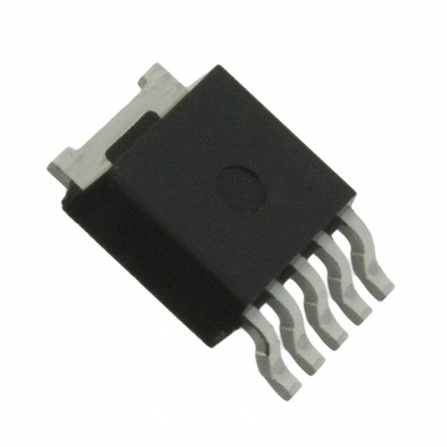


 工商网监
湘ICP备2023018690号
工商网监
湘ICP备2023018690号
