NJM2856
LOW DROPOUT VOLTAGE REGULATOR
GENERAL DESCRIPTION
The NJM2856 is a low dropout voltage regulator
with ON/OFF control.
Advanced Bipolar technology achieves low noise,
high ripple rejection.
It delivers up to 1A output power with the maximum
input voltage tolerance of 10V.
The package option is high power package as TO252-5
and HSOP8.
The NJM2856 is suitable for various applications
such as portable / consumer equipments.
PACKAGE OUTLINE
NJM2856DL3
NJM2856GM1
FEATURES
High Ripple Rejection
75dB typ. (f=1kHz,Vo=3V Version)
Output Noise Voltage
Vno=45µVrms typ.
Output capacitor with 2.2µF ceramic capacitor (Vo≥2.7V)
Output Current
Io(max.)=1A
High Precision Output
Vo±1.0%
Low Dropout Voltage
0.20V typ. (Io=600mA)
ON/OFF Control
Internal Short Circuit Current Limit
Internal Thermal Overload Protection
Bipolar Technology
Package Outline
TO-252-5 HSOP8
PIN CONFIGURATION
3
123 45
PIN CONFIGURATION
1. CONTROL
2. VIN
3. GND
4. Vo
5. NC
NJM2856DL3
8 7 6 5
Exposed Pad on
1 2 3 4 backside connected
NJM2856GM1 to GND
PIN CONFIGURATION
1. VOUT
2. N.C.
3. GND
4. N.C.
5. CONTROL
6. N.C.
7. N.C.
8. VIN
EQUIVALENT CIRCUIT
VIN
VOUT
Control
Thermal
Protection
Bandgap
Reference
GND
Ver.2011-04-04
1
�NJM2856
OUTPUT VOLTAGE RANK LIST
TO252-5 Package
Device Name
Vout
NJM2856DL3-15
NJM2856DL3-18
NJM2856DL3-23
NJM2856DL3-25
NJM2856DL3-03
NJM2856DL3-33
NJM2856DL3-05
1.5V
1.8V
2.3V
2.5V
3.0V
3.3V
5.0V
HSOP8 Package
2
Device Name
Vout
NJM2856GM1-15
NJM2856GM1-33
NJM2856GM1-05
1.5V
3.3V
5.0V
Ver.2011-04-04
�NJM2856
ABSOLUTE MAXIMUM RATINGS
PARAMETER
SYMBOL
Input Voltage
VIN
Control Voltage
VCONT
RATINGS
+10
+10
TO252-5
Power Dissipation
(Ta=25°C)
UNIT
V
V
PD
2-Layer(*1)
4-Layer (*2)
2-Layer (*1)
HSOP8
4-Layer (*2)
1190
3125
Unused Exposed PAD
Use Exposed PAD
Unused Exposed PAD
Use Exposed PAD
630
700
870
1700
mW
Operating
Topr
-40 ∼ +85
°C
Temperature
Storage
Tstg
-40 ∼ +150
°C
Temperature
(*1): Mounted on glass epoxy board. (76.2×114.3×1.6mm:EIA/JDEC standard size, 2Layers, copper area 100mm2)
(*2): Mounted on glass epoxy board. (76.2×114.3×1.6mm:EIA/JDEC standard size, 4Layers)
(4Layers inner foil: 74.2 x 74.2mm applying a thermal via hall to a board based on JEDEC standard JESD51-5)
OPERATING VOLTAGE
VIN=+2.5V ~ +8V (In case of Vo2.0V: VIN=VO+1V, VO≤2.0V: VIN=3.0V
The above specification is a common specification for all output voltages.
Therefore, it may be different from the individual specification for a specific output voltage.
Ver.2011-04-04
3
�NJM2856
POWER DISSIPATION vs. AMBIENT TEMPERATURE
NJM2856DL3 PowerDissipation
(Topr=-40~+85°C,Tj=150°C)
Power Dissipation P D(mW)
3500
3000
on 4 layers board
2500
2000
1500
on 2 layers board
1000
500
0
-50
-25
0
25
50
75
100
Temperature : Ta(°C)
NJM2856GM1 PowerDissipation
(Topr=-40~+85°C,Tj=150°C)
Power Dissipation PD(mW)
1800
on 4 layers board with Exposed PAD
1500
1200
on 4 layers board without Exposed PAD
900
on 2 layers board with Exposed PAD
600
on 2 layers board without Exposed PAD
300
0
-50
-25
0
25
50
75
100
Temperature : Ta(°C)
4
Ver.2011-04-04
�NJM2856
TEST CIRCUIT
A
IIN
VIN
VIN
0.33µF
A
V VCONT
*4
Ver.2011-04-04
ICONT
VOUT
NJM2856
2.2µF
*4
IOUT
V VOU
(ceramic)
CONTROL
GND
1.7V
很抱歉,暂时无法提供与“NJM2856DL3-15-TE1”相匹配的价格&库存,您可以联系我们找货
免费人工找货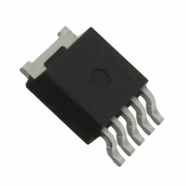


 工商网监
湘ICP备2023018690号
工商网监
湘ICP备2023018690号
