NJM2881/82
LOW DROPOUT VOLTAGE REGULATOR
GENERAL DESCRIPTION
NJM2881/82 is a low dropout voltage regulator with ON/OFF
control.
Advanced Bipolar technology achieves low noise, high ripple
rejection and low quiescent current.
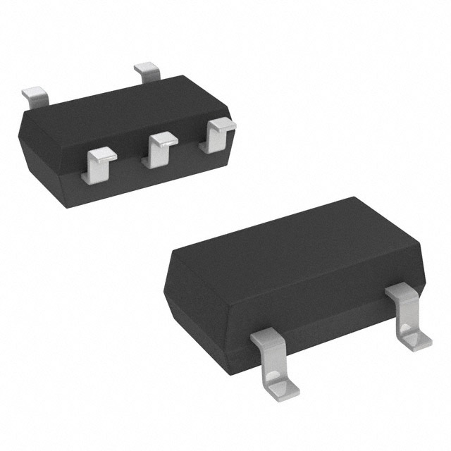
It is mounted on SOT-23-5 as small package and 1.0 F ceramic
capacitor is available. Therefore it is suitable for cellular phone,
camcorder, IC decoder, camera, and other portable items.
PACKAGE OUTLINE
NJM2881/82F
FEATURES
High Ripple Rejection
75dB typ. (f=1kHz ,Vo=3V version)
Low Output Noise Voltage Vno=30 Vrms (Cp=0.01 F)
Output capacitor with 1.0 F ceramic capacitor (Vo 2.7V)
Output Current
Io(max.)=300mA
High Precision Output
Vo 1.0%
Low Dropout Voltage
0.10V typ. (Io=100mA)
ON/OFF Control
(Active High)
Internal Short Circuit Current Limit
Internal Thermal Overload Protection
Bipolar Technology
Package Outline
SOT-23-5
PIN CONFIGURATION
5
4
1 2 3
1.
2.
3.
4.
5.
CONTROL (Active High)
GND
NOISE BYPASS
VOUT
VIN
NJM2881F
5
4
1 2 3
1.
2.
3.
4.
5.
VIN
GND
CONTROL (Active High)
NOISE BYPASS
VOUT
NJM2882F
BLOCK DIAGRAM
VIN
V OUT
Control
Thermal
Protection
Bandgap
Reference
Noise
Bypass
GND
Ver.2017-06-29
-1-
�NJM2881/82
OUTPUT VOLTAGE RANK LIST
Device Name
VOUT
Device Name
NJM288*F15
1.5V
NJM288*F29
NJM288*F17
1.7V
NJM288*F03
NJM288*F18
1.8V
NJM288*F31
NJM288*F21
2.1V
NJM288*F32
NJM288*F25
2.5V
NJM288*F33
NJM288*F28
2.8V
NJM288*F345
NJM288*F285
2.85V
NJM288*F35
VOUT
2.9V
3.0V
3.1V
3.2V
3.3V
3.45V
3.5V
Device Name
NJM288*F38
NJM288*F04
NJM288*F43
NJM288*F47
NJM288*F05
VOUT
3.8V
4.0V
4.3V
4.7V
5.0V
ABSOLUTE MAXIMUM RATINGS
PARAMETER
SYMBOL
Input Voltage
VIN
Control Voltage
VCONT
(Ta=25 C)
RATINGS
UNIT
+14
V
+14(*1)
V
350(*2)
Power Dissipation
PD
SOT-23-5
mW
200(*3)
Operating Temperature
Topr
-40 +85
C
Storage Temperature
Tstg
-40 +125
C
(*1): When input voltage is less than +14V, the absolute maximum control voltage is equal to the input voltage.
(*2): Mounted on glass epoxy board based on EIA/JEDEC. (114.3x76.2x1.6mm: 2Layers)
(*3): Device itself.
Operating voltage
VIN=+2.3 +6V (In case of Vo2.0V version: VIN=Vo+1V, CIN=0.1 F, Co=1.0 F: Vo 2.7V (Co=2.2 F: Vo 2.6V), Cp=0.01 F, Ta=25 C)
PARAMETER
SYMBOL
Output Voltage
Vo
Quiescent Current
Quiescent Current
at Control OFF
Output Current
Line Regulation
IQ
Load Regulation
Dropout Voltage
Ripple Rejection
IQ(OFF)
Io
Vo/ VIN
Vo/ Io
VI-O
RR
MIN.
TYP.
MAX.
UNIT
Io=30mA
Io=0mA, except Icont
VCONT=0V
TEST CONDITION
-1.0%
-
+1.0%
V
-
120
180
A
-
-
100
nA
Vo-0.3V
300
-
400
-
0.10
mA
%/V
-
0.10
0.03
0.18
%/mA
V
-
75
-
dB
-
ppm/ C
VIN=Vo+1V Vo+6V, Io=30mA
Io=0 300mA
Io=100mA
ein=200mVrms,f=1kHz,Io=10mA,
Vo=3V version
Ta=0 85 C, Io=10mA
Average Temperature
Coefficient of Output
Voltage
Output Noise Voltage
Control Voltage for ON-state
VCONT(ON)
1.6
30
-
-
Vrms
V
Control Voltage for OFF-state
VCONT(OFF)
-
-
0.6
V
-2-
Vo/ Ta
VNO
f=10Hz 80kHz, Io=10mA, Vo=3V version
-
50
Ver.2017-06-29
�NJM2881/82
ELECTRICAL CHARACTERISTICS
(Vo 2.0V version: VIN=Vo+1V, CIN=0.1 F, Co=2.2 F: Vo 1.9V (Co=4.7 F: Vo 1.8V), Cp=0.01 F, Ta=25 C)
PARAMETER
SYMBOL
TEST CONDITION
MIN.
TYP.
MAX.
UNIT
-1.0%
-
+1.0%
V
Output Voltage
Vo
Io=30mA
Quiescent Current
Quiescent Current
at Control OFF
Output Current
Line Regulation
IQ
Io=0mA, except ICONT
-
120
180
A
IQ(OFF)
VCONT=0V
-
-
100
nA
Io
Vo/ VIN
Vo-0.3V
VIN=Vo+1V Vo+6V, Io=30mA
300
-
400
-
0.10
mA
%/V
Load Regulation
Vo/ Io
-
-
0.03
%/mA
Ripple Rejection
RR
Io=0 300mA
ein=200mVrms,f=1kHz,Io=10mA,
Vo=1.8V version
-
80
-
dB
Ta=0 85 C, Io=10mA
-
-
ppm/ C
Average Temperature
Coefficient of Output Voltage
Output Noise Voltage
Control Voltage for ON-state
VNO
VCONT(ON)
Control Voltage for OFF-state
VCONT(OFF)
Vo/ Ta
f=10Hz 80kHz, Io=10mA, Vo=1.8V version
50
1.6
20
-
-
Vrms
V
-
-
0.6
V
The above specification is a common specification for all output voltages.
Therefore, it may be different from the individual specification for a specific output voltage.
TEST CIRCUIT
IIN
A
VIN
VOUT
IOUT
VIN
0.1 F
A
V
VCONT
ICONT
NJM2881/82
CONTROL
GND
NOISE
BYPASS
V
VOUT
1.0 F *4
(ceramic)
Cp=0.01 F
*4 1.9V Vo 2.6V version: Co=2.2 F(ceramic)
Vo 1.8V version: Co=4.7 F(ceramic)
Ver.2017-06-29
-3-
�NJM2881/82
TYPICAL APPLICATION
In the case where ON/OFF Control is not required:
VIN
VOUT
VOUT
VIN
0.1 F
1.0 F *5
NJM2881/82
R
(0 300k )
NOISE
BYPASS
CONTROL
Cp=0.01 F
GND
*5 1.9V Vo 2.6V version: Co=2.2 F
Vo 1.8V version: Co=4.7 F
Connect control terminal to VIN terminal
In use of ON/OFF CONTROL:
VIN
VIN
NJM2881/82
0.1 F
VOUT
VOUT
1.0 F *5
R
CONTROL
GND
NOISE
BYPASS
Cp=0.01 F
*5 1.9V Vo 2.6V version: Co=2.2 F
Vo 1.8V version: Co=4.7 F
State of control terminal:
“H” output is enabled.
“L” or “open” output is disabled.
*Noise bypass Capacitance Cp
Noise bypass capacitance Cp reduces noise generated by band-gap reference circuit. Noise level and ripple rejection
will be improved when larger Cp is used. Use of smaller Cp value may cause oscillation.
Use the Cp value of 0.01μF greater to avoid the problem.
*In the case of using a resistance "R" between VIN and control.
If this resistor is inserted, the control current could be reduced when the control voltage is high.
The applied voltage to control pin should set to consider voltage drop through the resistor “R” and the minimum
control voltage for ON-state.
The VCONT (ON) and ICONT have temperature dependence as shown in the "Control Current vs. Temperature" and "
Control Voltage vs. Temperature" characteristics. Therefore, the resistor "R" should be selected to consider the
temperature characteristics.
-4-
Ver.2017-06-29
�NJM2881/82
*Input Capacitor CIN
The input capacitor CIN is required in order to prevent oscillation and reduce power supply ripple of applications when
high power supply impedance or a long power supply line.
Therefore, the recommended capacitance (refer to conditions of ELECTRIC CHARACTERISTIC) or larger input
capacitor, connected between VIN and GND as short path as possible, is recommended in order to avoid the problem.
*Output Capacitor CO
The output capacitor CO is required for a phase compensation of the internal error amplifier, and the capacitance and
the equivalent series resistance (ESR) influence stable operation of the regulator.
If use a smaller output capacitor than the recommended capacitance (refer to conditions of ELECTRIC
CHARACTERISTIC), it may cause excess output noise or oscillation of the regulator due to lack of the phase
compensation. Therefore, the recommended capacitance or larger output capacitor, connected between VOUT and
GND as short path as possible, is recommended for stable operation. The recommended capacitance may be
different by output voltage, therefore confirm the recommended capacitance of the required output voltage.
Furthermore, a larger output capacitor reduces output noise and ripple output, and also improves Output Transient
Response when a load changes rapidly.
Selecting the output capacitor, should consider varied characteristics of a capacitor: frequency characteristics,
temperature characteristics, DC bias characteristics and so on. Therefore, the capacitor that has a sufficient margin of
the rated voltage against the output voltage and superior temperature characteristics, is recommended for CO.
Ver.2017-06-29
-5-
�NJM2881/82
POWER DISSIPATION vs. AMBIENT TEMPERATURE
NJM2881/82F Power Dissipation
(Topr=-40~+85℃,Tj=125℃,PD =200mW(Ta≦25℃))
Power Dissipation PD (mW)
500
On Board(114.3×76.2×1.6mm, FR-4)
400
300
Device itself
200
100
0
-50
-25
0
25
50
75
100
Ambient Temperature Ta(℃)
-6-
Ver.2017-06-29
�NJM2881/82
ELECTRICAL CHARACTERISTICS
NJM2881/82_3.0V
Output Voltage v.s. Input Voltage
NJM2881/82_3.0V
Output Voltage vs. Output Current
3.5
o
@:Ta=25 C
Co=1.0 F(Ceramic)
Cp=0.01 F
3
3.2
Output Voltage :Vo [V]
Output Voltage :Vo [V]
3.4
Io=0A
3
2.8
Io=100mA
2.5
2
1.5
1
o
@:Ta=25 C
Co=1.0 F(Ceramic)
Cp=0.01 F
0.5
Io=300mA
2.6
0
2.6
2.8
3
3.2
3.4
0
100
200
Input Voltage :Vin [V]
NJM2881/82_3.0V
Ground Pin Current vs. Output Current
20
400
500
600
NJM2881/82_3.0V
Dropout Voltage vs. Output Current
0.3
o
@:Ta=25 C
Co=1.0 F(Ceramic)
Cp=0.01 F
o
@:Ta=25 C
Co=1.0 F(Ceramic)
Cp=0.01 F
0.25
15
Dropout Voltage :dVi-o [V]
Ground Pin Current :IGND [mA]
300
Output Current :Io [mA]
10
5
0.2
0.15
0.1
0.05
0
0
0
100
200
300
400
500
0
100
NJM2881/82_3.0V
Control Current v.s. Control Voltage
20
200
300
400
500
Output Current :Io [mA]
Output Current :Io [mA]
NJM2881/82_3.0V
Output Voltage v.s. Control Voltage
4
o
3.5
15
Output Voltage :Vo [V]
Control Current :ICONT [ A]
@:Ta=25 C
Co=1.0 F(Ceramic)
Cp=0.01 F
Io=30mA
10
Rc=100k
Rc=50k
Rc=0
5
3
Rc=0
2.5
Rc=50k
2
Rc=100k
1.5
1
o
@:Ta=25 C
Vin=4.0V
Co=1.0 F(Ceramic)
Cp=0.01 F
Io=30mA
0.5
0
0
0
0.5
1
1.5
2
Control Voltage :VCONT [V]
Ver.2017-06-29
2.5
3
0
0.5
1
1.5
2
2.5
3
Control Voltage :VCONT [V]
-7-
�NJM2881/82
ELECTRICAL CHARACTERISTICS
NJM2881/82_3.0V
Peak Output Current vs. Input Voltage
NJM2881/82_3.0V
Load Regulation vs. Output Current
0
1000
800
Peak Output Current :Io MAX [mA]
Load Regulation :dVo/dIo [mV]
-10
-20
-30
-40
o
@:Ta=25 C
VIN=4V
Co=1.0 F(Ceramic)
Cp=0.01 F
-50
400
200
o
@:Ta=25 C
Co=1.0 F(Ceramic)
Cp=0.01 F
-60
0
600
100
200
300
400
0
500
4
6
8
Output Current :Io [mA]
10
NJM2881/82_3.0V
Quiescent Current v.s. Input Voltage
2000
o
@:Ta=25 C
VIN=4V
Co=1.0 F(Ceramic)
Io=10mA
Output Noise Voltage : Vn ( Vrms)
Quiescent Current : Iq [ A]
o
@:Ta=25 C
Output is open.
Co=1.0 F(Ceramic)
Cp=0.01 F
including Icont
1200
800
400
0
0
5
10
150
100
50
0
0.000001
15
20
Io=10mA
Io=30mA
60
40
o
@:Ta=25 C
VIN=4.0V
ein=200mVrms
Co=1.0 F(Ceramic)
Cp=0.01 F
20
0
1
Output Current :Io [mA]
-8-
0.1
80
40
0.1
0.01
Io=0mA
Ripple Rejection Ratio :RR [dB]
Output Noise Voltage :Vn [ Vrms]
@:Ta=25 C
VIN=4V
Co=1.0 F(Ceramic)
Cp=0.01 F
0.01
0.001
100
60
0
0.001
0.0001
NJM2881/82_3.0V
Ripple Rejection Ratio v.s. Frequency
NJM2881/82_3.0V
Output Noise Voltage vs. Output Current
o
80
0.00001
Noise Bypass Capacitor : Cp( F)
Input Voltage :Vin [V]
100
14
NJM2881/82_3.0V
Output Noise Voltage vs. Noise Bypass Capacitor
200
1600
12
Input Voltage :Vin [V]
10
100
10
10
100
1k
1000
4
10k
10
5
100k
10
Frequency :f [Hz]
Ver.2017-06-29
�NJM2881/82
ELECTRICAL CHARACTERISTICS
NJM2881/82_3.0V
Equivalent Series Resistance vs. Output Current
NJM2881/82_3.0V
Ripple Rejection vs. Output Current
100
100
o
Equivalent Series Resistance :ESR [ ]
f=1kHz
Ripple Rejection : RR (dB)
80
60
f=10kHz
40
o
@:Ta=25 C
VIN=4.0V
ein=200mVrms
Co=1.0 F(Ceramic)
Cp=0.01 F
20
0
0.001
@:Ta=25 C
VIN=4V
Co=1.0 F(Ceramic)
Cp=0.01 F
10
STABLE REGION
1
0.1
0.02
0.01
0.1
1
10
100
0.001
1000
0.01
0.1
Output Current : Io(mA)
1
10
100
1000
Output Current :Io [mA]
NJM2881/82_3.0V
ƒf [ƒ^
Dropout Voltage
v.s.1Temperature
NJM2881/82_3.0V
Output Voltage v.s. Temperature
3.1
0.3
@:VIN=4V
Io=30mA
Co=1.0 F(Ceramic)
Cp=0.01 F
@:Io=100mA
Co=1.0 F(Ceramic)
Cp=0.01 F
0.25
Output Voltage :Vo [V]
Dropout Voltage : Vi-o [V]
3.05
0.2
0.15
0.1
3
2.95
0.05
2.9
0
-50
0
50
100
-50
150
0
100
150
Temperature :Ta [ C]
NJM2881/82_3.0V
Control Voltage v.s. Temperature
NJM2881/82_3.0V
Control Current v.s. Temperature
10
2
@:VIN=4V
Output is open.
Co=1.0 F(Ceramic)
Cp=0.01 F
@:VIN=4V
Output is open.
Co=1.0 F(Ceramic)
Cp=0.01 F
V CONT=1.6V
8
1.5
Control Current : ICONT ( A)
Control Voltage :Vcont-off [V]
50
o
o
Temperature :Ta [ C]
1
0.5
6
4
2
0
-50
0
50
o
Temperature :Ta [ C]
Ver.2017-06-29
100
150
0
-50
0
50
o
100
150
Temperature Ta ( C)
-9-
�NJM2881/82
ELECTRICAL CHARACTERISTICS
NJM2881/82_3.0V
Quiescent Current v.s. Temperature
NJM2881/82_3.0V
Short Circuit Current v.s. Temperature
300
200
@:VIN=4V
Output is open
Co=1.0 F(Ceramic)
Cp=0.01 F
Include Icont
Short Circuit Current :Isc [mA]
Quiescent Current : Iq [ A]
250
@:VIN=4.0V
Output is short to ground.
Co=1.0 F(Ceramic)
Cp=0.01 F
200
150
100
150
100
50
50
0
0
-50
0
50
100
-50
150
0
100
150
Temperature :Ta [ C]
NJM2881/82_3.0V
Load Regulation v.s. Temperature
NJM2881/82_3.0V
Line Regulation v.s. Temperature
0.03
0.2
@:VIN=4.0-9.0V
Io=30mA
Co=1.0 F(Ceramic)
Cp=0.01 F
@:VIN=4.0V
Io=0-100mA
Co=1.0 F(Ceramic)
Cp=0.01 F
0.025
Load Regulation :dVo/dIo [%/mA]
Line Regulation :dVo/dVin [%/V]
50
o
o
Temperature :Ta [ C]
0.1
0
-0.1
-0.2
0.02
0.015
0.01
0.005
0
-50
0
50
100
150
o
-50
0
50
100
150
o
Temperature :Ta [ C]
Temperature :Ta [ C]
NJM2881/82_3.0V
Output Voltage v.s. Temperature
3.5
3
Output Voltage :Vo [V]
2.5
2
1.5
1
@:VIN=4.0V
Io=30mA
Co=1.0 F(Ceramic)
Cp=0.01 F
0.5
0
-50
0
50
100
150
200
o
Temperature :Ta [ C]
- 10 -
Ver.2017-06-29
�NJM2881/82
ELECTRICAL CHARACTERISTICS
NJM2881_3.0V
ON/OFF Transient Response
NJM2881_3.0V
ON/OFF Transient Response without Load
20
10
5
6
0
-5
4
Output Voltage
Output Voltage : Vo [V]
10
Control Voltage
8
@:Ta=25 C
VDD =4.0V
Co=1.0 F(Ceramic)
Cp=0.01 F
Io=30mA
15
Control Voltage : Vo [V]
15
10
Control Voltage
8
5
6
0
-5
4
Output Voltage
-10
2
-10
2
-15
-15
0
0
-20
0
1
2
3
Time : t [S]
4
-20
5
0
4
8
NJM2881/82_3.0V
Load Transient Response
12
Time : t [ mS]
400
3.12
10
o
o
3.1
300
3.08
3.06
250
3.04
200
3.02
150
Output Voltage
3
100
2.98
2.96
0
40
80
120
Time : t [ S]
160
200
Output Voltage : Vo [V]
Output Voltage : Vo [V]
3.08
350
Output Current : Io [mA]
@:Ta=25 C
VDD =4.0V
Co=1.0 F(Ceramic)
Cp=0.01 F
Output Current
20
NJM2881/82_3.0V
Input Transient Response
3.12
3.1
16
@:Ta=25 C
VDD =4.0V
Co=1.0 F(Ceramic)
Cp=0.01 F
Io=30mA
8
6
Input Voltage
3.06
4
3.04
2
3.02
Output Voltage
0
3
50
2.98
0
2.96
Input Voltage : VIN [V]
Output Voltage : Vo [V]
10
20
o
12
Control Voltage : Vo [V]
@:Ta=25oC
V DD =4.0V
Co=1.0 F(Ceramic)
Cp=0.01 F
Io=0mA
12
-2
-4
0
40
80
120
Time : t [ S]
160
200
[CAUTION]
The specifications on this databook are only
given for information , without any guarantee
as regards either mistakes or omissions. The
application circuits in this databook are
described only to show representative usages
of the product and not intended for the
guarantee or permission of any right including
the industrial rights.
Ver.2017-06-29
- 11 -
�


 工商网监
湘ICP备2023018690号
工商网监
湘ICP备2023018690号
