NJW4170
Current Mode Control High Speed Frequency
Internal 1A MOSFET Switching Regulator IC for Buck Converter
GENERAL DESCRIPTION
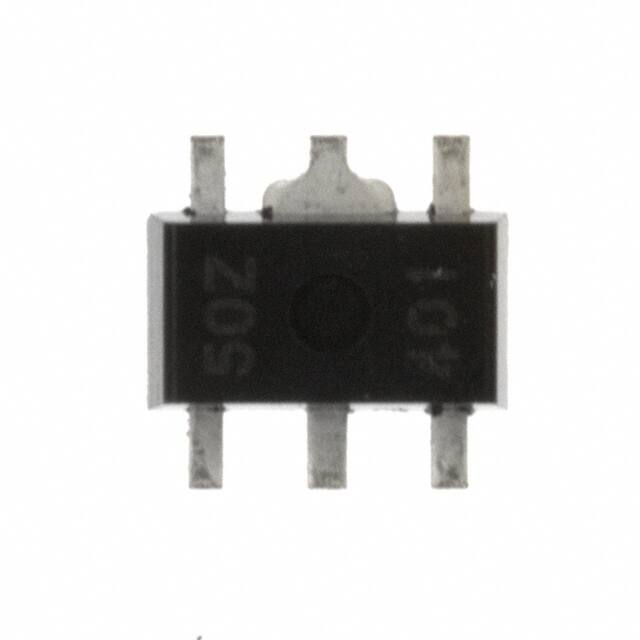
■ PACKAGE OUTLINE
The NJW4170 is a high speed oscillating frequency buck
converter with 40V/1A MOSFET. Current mode control and built-in
phase compensation circuit minimize external parts and contribute
to using a Low ESR Output Capacitor(MLCC) within wide input
range from 4.5V to 40V. Therefore, the NJW4170 can realize
downsizing of applications.
Also, it has a soft start function, an external clock synchronization
function, an over current protection and a thermal shutdown circuit.
Over 2MHz of Switching frequency can avoid interference with
the AM radio frequency.
It is suitable for supplying power to a Car Accessory, Audio
Automation Equipment, Industrial Instrument and so on.
FEATURES
Oscillating Frequency
NJW4170U2
NJW4170KV1
2.4MHz typ. (A ver.)
2.1MHz typ. (B ver.)
80ns typ.(A ver.)
85ns typ.(B ver.)
Minimum ON time
Current mode Control
External Clock Synchronization
Wide Operating Voltage Range
4.5V to 40V
Switching Current
1.4A min.
PWM Control
Built-in Compensation Circuit
Correspond to Ceramic Capacitor (MLCC)
Soft Start Function
4ms typ.
UVLO (Under Voltage Lockout)
Over Current Protection (Hiccup type)
Thermal Shutdown Protection
Standby Function
Package Outline
NJW4170U2 : SOT-89-5
NJW4170KV1 : DFN8-V1(ESON8-V1)
PRODUCT CLASSIFICATION
Version
Oscillating
Frequency
Package
NJW4170U2-A
A
2.4MHz typ.
SOT-89-5
NJW4170KV1-A
A
2.4MHz typ.
DFN8-V1
(ESON8-V1)
NJW4170U2-B
B
2.1MHz typ.
SOT-89-5
Part Number
Ver.2020-09-14
Operating
Temperature Range
General Spec.
-40 C to +125 C
General Spec.
-40 C to +125 C
General Spec.
-40 C to +125 C
-1-
�NJW4170
PIN CONFIGURATION
5 V+
EN/SYNC 1
GND 2
(2) GND
IN- 3
SW
N.C.
V+
N.C.
1
2
3
4
8
7
6
5
INN.C.
GND
EN/SYNC
4 SW
8
7
6
5
1
2
3
4
Exposed PAD on backside
connect to GND.
(Top View)
(Bottom View)
NJW4170KV1
NJW4170U2
PIN DESCRIPTIONS
PIN NAME
PIN NUMBER
DFN8-V1
SOT-89-5
(ESON8)
EN/SYNC
1
5
GND
2
6
IN-
3
8
SW
V+
N.C.
Exposed
PAD
4
5
–
1
3
2, 4, 7
–
–
-2-
FUNCTION
Standby Control pin
The EN/SYNC pin internally pulls down with 100k . Normal
Operation at the time of High Level. Standby Mode at the time of
Low Level or OPEN.
Moreover, it operates by inputting clock signal at the oscillatory
frequency that synchronized with the input signal.
GND pin
Output Voltage Detecting pin
Connects output voltage through the resistor divider tap to this pin in
order to voltage of the IN- pin become 0.8V.
Switch Output pin of Power MOSFET
Power Supply pin for Power Line
Non connection
Connect to GND (Only DFN8-V1 PKG)
Ver.2020-09-14
�NJW4170
BLOCK DIAGRAM
V+
SLOPE
COMP.
CURRENT
SENSE
UVLO
OCP
EN/SYNC
High: ON
Low: OFF(Standby)
Enable
(Standby)
SYNC
OSC
S Q
Buffer
R
SW
TSD
PWM
INER·AMP
Soft Start
Vref
0.8V
GND
Ver.2020-09-14
-3-
�NJW4170
ABSOLUTE MAXIMUM RATINGS
PARAMETER
SYMBOL
Supply Voltage
V+
V+- SW pin Voltage
VV-SW
EN/SYNC pin Voltage
VEN/SYNC
IN- pin Voltage
VINPower Dissipation
Junction Temperature Range
Operating Temperature Range
Storage Temperature Range
PD
MAXIMUM RATINGS
-0.3 to +45
+45
-0.3 to +45
-0.3 to +6
625 (*1)
SOT-89-5
2,400 (*2)
mW
DFN8-V1
(ESON8-V1)
Tj
Topr
Tstg
(Ta=25°C)
UNIT
V
V
V
V
600 (*3)
1,800 (*4)
-40 to +150
-40 to +125
-50 to +150
C
C
C
(*1): Mounted on glass epoxy board. (76.2×114.3×1.6mm:based on EIA/JDEC standard size, 2Layers, Cu area 100mm2)
(*2): Mounted on glass epoxy board. (76.2×114.3×1.6mm:based on EIA/JDEC standard, 4Layers)
(For 4Layers: Applying 74.2×74.2mm inner Cu area and a thermal via hall to a board based on JEDEC standard JESD51-5)
(*3): Mounted on glass epoxy board. (101.5 114.5 1.6mm: based on EIA/JEDEC standard, 2Layers FR-4, with Exposed Pad)
(*4): Mounted on glass epoxy board. (101.5 114.5 1.6mm: based on EIA/JEDEC standard, 4Layers FR-4, with Exposed Pad)
(For 4Layers: Applying 99.5 99.5mm inner Cu area and a thermal via hole to a board based on JEDEC standard JESD51-5)
RECOMMENDED OPERATING CONDITIONS
PARAMETER
SYMBOL
Supply Voltage
V+
External Clock Input Range
A version
fSYNC
B version
-4-
MIN.
4.5
TYP.
–
MAX.
40
UNIT
V
2.3
2.0
–
–
2.8
2.5
MHz
Ver.2020-09-14
�NJW4170
(Unless otherwise noted, V+=VEN/SYNC=12V, Ta=25 C)
ELECTRICAL CHARACTERISTICS
PARAMETER
SYMBOL
Under Voltage Lockout Block
ON Threshold Voltage
OFF Threshold Voltage
Hysteresis Voltage
VT_ON
VT_OFF
VHYS
tSS
Soft Start Block
Soft Start Time
TEST CONDITION
MIN.
TYP.
MAX.
UNIT
V+= L → H
V+= H → L
4.2
4.11
70
4.35
4.26
90
4.5
4.41
–
V
V
mV
VB=0.75V
2.5
4
8
ms
A version, VIN-=0.7V
B version, VIN-=0.7V
A version, VIN-=0.2V
B version, VIN-=0.2V
2.2
1.9
–
–
2.4
2.1
340
290
2.6
2.3
–
–
MHz
MHz
kHz
kHz
Oscillator Block
Oscillating Frequency
Oscillating Frequency
(Low Frequency Control)
Oscillating Frequency
deviation (Supply voltage)
Oscillating Frequency
deviation (Temperature)
Error Amplifier Block
Reference Voltage
Input Bias Current
PWM Comparate Block
Maximum Duty Cycle
Minimum ON Time1
(Use Built-in Oscillator)
Minimum ON Time2
(Use Ext CLK)
Ver.2020-09-14
fOSC
fOSC_LOW
fDV
V+=4.5 to 40V
–
1
–
%
fDT
Ta= -40 C to +85 C
–
5
–
%
-1.0%
-0.1
0.8
–
+1.0%
+0.1
V
A
77.5
–
–
–
–
82
80
85
80
85
–
115
120
115
120
%
ns
ns
ns
ns
VB
IB
MAXDUTY
tON-min1
tON-min2
A, B version, VIN-=0.7V
A version
B version
A version, fSYNC =2.6kHz
B version, fSYNC =2.3kHz
-5-
�NJW4170
(Unless otherwise noted, V+=VEN/SYNC=12V, Ta=25 C)
ELECTRICAL CHARACTERISTICS
PARAMETER
SYMBOL
Over Current Protection Block
Cool Down Time
tCOOL
Output Block
Output ON Resistance
Switching Current Limit
SW Leak Current
RON
ILIM
ILEAK
Standby Control / Sync Block
EN/SYNC pin
High Threshold Voltage
EN/SYNC pin
Low Threshold Voltage
Input Bias Current
(EN/SYNC pin)
MIN.
TYP.
MAX.
UNIT
–
75
–
ms
VEN/SYNC=0V, V+=40V, VSW=0V
–
1.4
–
0.4
1.9
–
0.65
2.4
1
A
A
VTHH_EN/SYNC
VEN/SYNC= L → H
1.6
–
V+
V
VTHL_EN/SYNC
VEN/SYNC= H → L
0
–
0.5
V
VEN/SYNC=12V
–
270
390
A
–
2.0
2.4
mA
–
–
1
A
IEN
TEST CONDITION
ISW=1A
General Characteristics
Quiescent Current
Standby Current
-6-
IDD
IDD_STB
A, B version,
RL=no load, VIN-=0.9V
VEN/SYNC=0V
Ver.2020-09-14
�NJW4170
POWER DISSIPATION vs. AMBIENT TEMPERATURE
NJW4170KV1 (DFN8-V1 Package)
Power Dissipation vs. Ambient Temperature
(Tj=~150°C)
NJW4170U2 (SOT89-5 Package)
Power Dissipation vs. Ambient Temperature
(Tj=~150°C)
3000
At on 4 layer PC Board (*6)
At on 2 layer PC Board (*5)
2500
Power Dissipation PD (mW)
Power Dissipation PD (mW)
3000
2000
1500
1000
500
At on 4 layer PC Board (*8)
At on 2 layer PC Board (*7)
2500
2000
1500
1000
500
0
0
-50
-25
0
25
50
75
100
125
-50
150
-25
0
25
50
75
100
125
150
Ambient Temperature Ta (°C)
Ambient Temperature Ta (°C)
(*5): Mounted on glass epoxy board. (76.2×114.3×1.6mm:based on EIA/JDEC standard size, 2Layers, Cu area 100mm2)
(*6): Mounted on glass epoxy board. (76.2×114.3×1.6mm:based on EIA/JDEC standard, 4Layers)
(For 4Layers: Applying 74.2×74.2mm inner Cu area and a thermal via hall to a board based on JEDEC standard JESD51-5)
(*7): Mounted on glass epoxy board. (101.5 114.5 1.6mm: based on EIA/JEDEC standard, 2Layers FR-4, with Exposed Pad)
(*8): Mounted on glass epoxy board. (101.5 114.5 1.6mm: based on EIA/JEDEC standard, 4Layers FR-4, with Exposed Pad)
(For 4Layers: Applying 99.5 99.5mm inner Cu area and a thermal via hole to a board based on JEDEC standard JESD51-5)
TYPICAL APPLICATIONS
L
VIN
VOUT
CIN
V+
CFB
SW
R2
NJW4170
EN/
SYNC
GND
IN-
SBD
COUT
R1
EN/SYNC
High: ON
Low: OFF
(Standby)
Ver.2020-09-14
-7-
�NJW4170
TYPICAL CHARACTERISTICS (A, B version)
Reference Voltage vs. Supply Voltage
(Ta=25ºC)
Reference Voltage :VB (V)
0.81
0.805
0.8
0.795
0.79
Switching Current Limit :ILIM (A)
10
20
30
Supply Voltage :V+ (V)
0.795
40
-50
Switching Current Limit vs. Temperature
2.4
2.2
2
V+=12V
V+=40V
1.8
1.6
V+=5V
1.4
1.2
-25
0
25 50 75 100 125 150
Temperature : (ºC)
Output ON Resistance vs. Temperature
(ISW=1A)
0.8
0.7
0.6
0.5
0.4
V+=5V
V+=40V
V+=12V
0.3
0.2
0.1
0
-50
-25
0
25 50 75 100 125 150
Temperature : (ºC)
-50
-25
0
25 50 75 100 125 150
Temperature : (ºC)
Maximum Duty Cycle vs. Temperature
(V+=12V, VIN-=0.7V)
90
Maximum Duty Cycle :MAXDUTY (%)
0.8
0.79
0
2.6
0.805
Output ON Resistance :RON (Ω)
Reference Voltage :VB (V)
0.81
Reference Voltage vs. Temperature
(V+=12V)
88
86
84
82
80
78
76
-50
-8-
-25
0
25 50 75 100 125 150
Temperature : (ºC)
Ver.2020-09-14
�NJW4170
TYPICAL CHARACTERISTICS (A, B version)
Under Voltage Lockout Voltage vs. Temperature
4.5
8
Soft Start Time :tSS (ms)
Threshold Voltage : (V)
4.45
4.4
4.35
VT_ON
4.3
4.25
4.2
VT_OFF
4.1
6
5
4
2
-50
-25
0
25 50 75 100 125 150
Temperature : (ºC)
-50
Switching Leak Current vs. Temperature
(V+=40V, VEN/SYNC=0V, VSW=0V)
1.5
1
0.5
0
-25
0
25 50 75 100 125 150
Temperature : (ºC)
Standby Current vs. Temperature
(VEN/SYNC=0V)
1
Standby Current :IDD_STB (μA)
2
Switching Leak Current :ILEAK (μA)
7
3
4.15
0.8
0.6
0.4
V+=40V
V+=12V
V+=4.5V
0.2
0
-50
-25
0
25 50 75 100 125 150
Temperature : (ºC)
-50
Quiescent Current vs. Supply Voltage
(RL=no Load, VIN-=0.9V, Ta=25ºC)
3
2.5
2
1.5
1
0.5
0
-25
0
25 50 75 100 125 150
Temperature : (ºC)
Quiescent Current vs. Temperature
(RL=no Load, VIN-=0.9V)
3
Quiescent Current :IDD (mA)
Quiescent Current :IDD (mA)
Soft Start Time vs. Temperature
(V+=12V, VB=0.75V)
2.5
2
V+=4.5V, 12V, 40V
1.5
1
0.5
0
0
Ver.2020-09-14
10
20
30
Supply Voltage :V+ (V)
40
-50
-25
0
25 50 75 100 125 150
Temperature : (ºC)
-9-
�NJW4170
TYPICAL CHARACTERISTICS (A version)
Oscillating Frequency vs. Supply Voltage
(A ver., VIN-=0.7V, Ta=25ºC)
2.8
Oscillating Frequency :fOSC (MHz)
Oscillating Frequency :fOSC (MHz)
2.8
2.7
2.6
2.5
2.4
2.3
2.2
2.1
2
2.7
2.6
2.5
2.4
2.3
2.2
2.1
2
0
10
20
30
Supply Voltage : V+ (V)
40
-50
-25
0
25 50 75 100 125 150
Temperature : (ºC)
Minimum ON Time1 vs. Temperature
(A ver., V+=12V)
120
Minimum ON Time1 :tON-min1 (ns)
Oscillating Frequency vs Temperature
(A ver., V+=12V, VIN-=0.7V)
110
100
90
80
70
60
50
40
-50
- 10 -
-25
0
25 50 75 100 125 150
Temperature : (ºC)
Ver.2020-09-14
�NJW4170
TYPICAL CHARACTERISTICS (B version)
Oscillating Frequency vs. Supply Voltage
(B ver., VIN-=0.7V, Ta=25ºC)
2.4
Oscillating Frequency :fOSC (MHz)
Oscillating Frequency :fOSC (MHz)
2.4
2.3
2.2
2.1
2
1.9
1.8
2.3
2.2
2.1
2
1.9
1.8
0
10
20
30
Supply Voltage :V+ (V)
40
-50
-25
0
25 50 75 100 125 150
Temperature : (ºC)
Minimum ON Time1 vs. Temperature
(B ver., V+=12V)
120
Minimum ON Time1 :tON-min1 (ns)
Oscillating Frequency vs Temperature
(B ver., V+=12V, VIN-=0.7V)
110
100
90
80
70
60
50
40
-50
Ver.2020-09-14
-25
0
25 50 75 100 125 150
Temperature : (ºC)
- 11 -
�NJW4170
NJW4170Application Manual
Technical Information
Description of Block Features
1. Basic Functions / Features
Error Amplifier Section (ER AMP)
0.8V±1% precise reference voltage is connected to the non-inverted input of this section.
To set the output voltage, connects converter's output to inverted input of this section (IN- pin). If requires output
voltage over 0.8V, inserts resistor divider.
Because the optimized compensation circuit is built-in, the application circuit can be composed of minimum
external parts.
PWM Comparator Section (PWM), Oscillating Circuit Section (OSC)
The NJW4170 uses a constant frequency, current mode step down architecture. The oscillating frequency are
2.4MHz (typ.) at A version and 2.1MHz (typ.) at B version. The PWM signal is output by feedback of output voltage
and slope compensation switching current at the PWM comparator block.
The maximum duty ratio is 82% (typ.).
The minimum ON time are limited to 80ns (typ.) at A version and 85ns (typ.) at B version.
The buck converter of ON time is decided the following formula.
ton
VOUT
s
VIN fOSC
VIN shows input voltage and VOUT shows output voltage.
When the ON time becomes below in tON-min, in order to maintain output voltage at a stable state, change of duty or
pulse skip operation may be performed.
Power MOSFET (SW Output Section)
The power is stored in the inductor by the switch operation of built-in power MOSFET. The output current is limited
to 1.4A(min.) the overcurrent protection function. In case of step-down converter, the forward direction bias voltage is
generated with inductance current that flows into the external regenerative diode when MOSFET is turned off.
The SW pin allows voltage between the V+ pin and the SW pin up to +45V. However, you should use an Schottky
diode that has low saturation voltage.
Power Supply, GND pin (V+ and GND)
In line with switching element drive, current flows into the IC according to frequency. If the power supply
impedance provided to the power supply circuit is high, it will not be possible to take advantage of IC performance
due to input voltage fluctuation. Therefore insert a bypass capacitor close to the V+ pin – the GND pin connection in
order to lower high frequency impedance.
- 12 -
Ver.2020-09-14
�NJW4170 Application
Manual
NJW4170
Technical Information
Description of Block Features (Continued)
2. Additional and Protection Functions / Features
Under Voltage Lockout (UVLO)
The UVLO circuit operating is released above V+=4.35V(typ.) and IC operation starts. When power supply voltage
is low, IC does not operate because the UVLO circuit operates. There is 90mV(typ.) width hysteresis voltage at rise
and decay of power supply voltage. Hysteresis prevents the malfunction at the time of UVLO operating and
releasing.
Soft Start Function (Soft Start)
The output voltage of the converter gradually rises to a set value by the soft start function. The soft start time is
4ms (typ.). It is defined with the time of the error amplifier reference voltage becoming from 0V to 0.75V. The soft
start circuit operates after the release UVLO and/or recovery from thermal shutdown. The operating frequency is
controlled with a low frequency 340kHz (typ.) at A version and 290kHz (typ.) at B version, until voltage or the IN- pin
becomes approximately 0.4V.
0.8V
Vref,
IN- pin Voltage
OSC Waveform
ON
SW pin
OFF
UVLO(4.35V typ.) Release,
Standby,
Recover from Thermal
Shutdown
Low Frequency Control
VIN-=approx 0.4V
Soft Start time: Tss=4ms(typ.) to VB=0.75V
Steady
Operaton
Soft Start effective period to VB=0.8V
Fig. 1. Startup Timing Chart
Ver.2020-09-14
- 13 -
�NJW4170
NJW4170Application Manual
Technical Information
Description of Block Features (Continued)
Over Current Protection Circuit (OCP)
NJW4170 contains overcurrent protection circuit of hiccup architecture. The overcurrent protection circuit of hiccup
architecture is able to decrease heat generation at the overload.
The NJW4170 output returns automatically along with release from the over current condition.
At when the switching current becomes ILIM or more, the overcurrent protection circuit is stopped the MOSFET
output. The switching output holds low level down to next pulse output at OCP operating.
When IN- pin voltage becomes 0.3V or less, it operates with 340kHz (typ.) at A version and 290kHz (typ.) at B
version.
At the same time starts pulse counting, and stops the switching operation when the overcurrent detection
continues 128 pulses.
After NJW4170 switching operation was stopped, it restarts by soft start function after the cool down time of approx
75ms (typ.).
IN- pin
Voltage
0.8V
0.3V
0V
Oscillating Frequency
A ver.=2.4MHz typ.
B ver.=2.1MHz typ.
OCP Operates
Oscillating Frequency
A ver.=340kHz typ.
B ver.=290kHz typ.
ON
SW pin
OFF
Switching
Current
ILIM
0
Pulse by
Pulse
Static Status
Pulse Count :128 pulse
Cool Down time :75ms typ.
Detect
Overcurrent
Soft Start
Fig. 2. Timing Chart at Over Current Detection
Thermal Shutdown Function (TSD)
When Junction temperature of the NJW4170 exceeds the 165°C*, internal thermal shutdown circuit function stops
SW function. When junction temperature decreases to 150°C* or less, SW operation returns with soft start operation.
The purpose of this function is to prevent malfunctioning of IC at the high junction temperature. Therefore it is not
something that urges positive use. You should make sure to operate within the junction temperature range rated
(150 C). (* Design value)
Standby Function
The NJW4170 stops the operating and becomes standby status when the EN/SYNC pin becomes less than 0.5V.
The EN/SYNC pin internally pulls down with 100k , therefore the NJW4170 becomes standby mode when the
EN/SYNC pin is OPEN. You should connect this pin to V+ when you do not use standby function.
- 14 -
Ver.2020-09-14
�NJW4170 Application
Manual
NJW4170
Technical Information
Description of Block Features (Continued)
External Clock Synchronization
By inputting a square wave to EN/SYNC pin, can be synchronized to an external frequency.
You should fulfill the following specification about a square wave. (Table 1.)
Table 1. The input square wave to an EN/SYNC pin.
A version
B version
(fOSC =2.4MHz)
(fOSC =2.1MHz)
Input Frequency
2.3MHz to 2.8MHz
2.0MHz to 2.5MHz
Duty Cycle
40% to 60%
Voltage
1.6V or more at High level
magnitude
0.5V or less at Low level
The trigger of the switching operating at the external synchronized mode is detected to the rising edge of the input
signal. At the time of switching operation from standby or asynchronous to synchronous operation, it has set a delay
time approx 5 s to 10 s in order to prevent malfunctions. (Fig. 3.)
High
EN/SYNC pin
Low
ON
SW pin
OFF
Standby
Delay Time
External Clock Synchronization
Fig. 3. Switching Operation by External Synchronized Clock
Ver.2020-09-14
- 15 -
�NJW4170
NJW4170Application Manual
Technical Information
Application Information
Inductors
Because a large current flows to the inductor, you should select the inductor with the large current capacity not to
saturate. Optimized inductor value is determined by the input voltage and output voltage.
Reducing L decreases the size of the inductor. However a peak current increases and adversely affects the
efficiency. (Fig. 4.)
Moreover, you should be aware that the output current is limited because it becomes easy to operating to the
overcurrent limit.
The peak current is decided the following formula.
IL
Ipk
VIN VOUT VOUT
[A]
L VIN fOSC
IL
[A]
2
IOUT
Current
Peak Current IPK
Indunctor
Ripple Current IL
Peak Current IPK
Output Current
IOUT
Indunctor
Ripple Current IL
0
tON
tOFF
Reducing L Value
tON
tOFF
Increasing L value
Fig. 4. Inductor Current State Transition (Continuous Conduction Mode)
- 16 -
Ver.2020-09-14
�NJW4170 Application
Manual
NJW4170
Technical Information
Application Information (Continued)
Input Capacitor
Transient current flows into the input section of a switching regulator responsive to frequency. If the power supply
impedance provided to the power supply circuit is large, it will not be possible to take advantage of the NJW4170
performance due to input voltage fluctuation. Therefore insert an input capacitor as close to the MOSFET as
possible. A ceramic capacitor is the optimal for input capacitor.
The effective input current can be expressed by the following formula.
IRMS
VOUT
IOUT
VIN
VIN
VOUT
[A]
In the above formula, the maximum current is obtained when VIN = 2 VOUT, and the result in this case is
IRMS = IOUT (MAX) 2.
When selecting the input capacitor, carry out an evaluation based on the application, and use a capacitor that has
adequate margin.
Output Capacitor
An output capacitor stores power from the inductor, and stabilizes voltage provided to the output.
Because NJW4170 corresponds to the output capacitor of low ESR, the ceramic capacitor is the optimal for
compensation.
In addition, you should consider varied characteristics of capacitor (a frequency characteristic, a temperature
characteristic, a DC bias characteristic and so on) and unevenness peculiar to a capacitor supplier enough.
Therefore when selecting a capacitors, you should confirm the characteristics with supplier datasheets.
When selecting an output capacitor, you must consider Equivalent Series Resistance (ESR) characteristics, ripple
current, and breakdown voltage.
The output ripple noise can be expressed by the following formula.
Vripple( p
p)
IL
ESR
1
8 fOSC C OUT
[V]
The effective ripple current that flows in a capacitor (Irms) is obtained by the following equation.
Irms
Ver.2020-09-14
IL
2 3
[ Arms]
- 17 -
�NJW4170
NJW4170Application Manual
Technical Information
Application Information (Continued)
Catch Diode
When the switch element is in OFF cycle, power stored in the inductor flows via the catch diode to the output
capacitor. Therefore during each cycle current flows to the diode in response to load current. Because diode's
forward saturation voltage and current accumulation cause power loss, a Schottky Barrier Diode (SBD), which has a
low forward saturation voltage, is ideal.
An SBD also has a short reverse recovery time. If the reverse recovery time is long, through current flows when
the switching transistor transitions from OFF cycle to ON cycle. This current may lower efficiency and affect such
factors as noise generation.
Setting Output Voltage, Compensation Capacitor
The output voltage VOUT is determined by the relative resistances of R1, R2. The current that flows in R1, R2 must
be a value that can ignore the bias current that flows in ER AMP.
R2
R1
VOUT
1
VB [ V ]
The zero points are formed with R2 and CFB, and it makes for the phase compensation of NJW4170.
The zero point is shown the following formula.
f Z1
2
1
[Hz]
R 2 C FB
You should set the zero point as a guide from 60kHz to 80kHz.
- 18 -
Ver.2020-09-14
�NJW4170 Application
Manual
NJW4170
Technical Information
Application Information (Continued)
Board Layout
In the switching regulator application, because the current flow corresponds to the oscillating frequency, the
substrate (PCB) layout becomes an important.
You should attempt the transition voltage decrease by making a current loop area minimize as much as possible.
Therefore, you should make a current flowing line thick and short as much as possible. Fig.5. shows a current loop
at step-down converter. Especially, should lay out high priority the loop of CIN-SW-SBD that occurs rapid current
change in the switching. It is effective in reducing noise spikes caused by parasitic inductance.
NJW4170
Built-in SW
VIN
CIN
NJW4170
Built-in SW
L
SBD
COUT
VIN
CIN
(a) Buck Converter SW ON
L
SBD
COUT
(b) Buck Converter SW OFF
Fig. 5. Current Loop at Buck Converter
Concerning the GND line, it is preferred to separate the power system and the signal system, and use single
ground point.
The voltage sensing feedback line should be as far away as possible from the inductance. Because this line has
high impedance, it is laid out to avoid the influence noise caused by flux leaked from the inductance.
Fig. 6. shows example of wiring at buck converter. Fig. 7 shows the PCB layout example.
L
V+
VIN
VOUT
SW
CIN
SBD
COUT
RL
The capacitor is
connected near an IC.
NJW4170
CFB
INR2
GND
Separate Digital(Signal)
GND from Power GND
R1
To avoid the influence of the voltage
drop, the output voltage should be
detected near the load.
Because IN- pin is high impedance, the
voltage detection resistance: R1/R2 is
put as much as possible near IC(IN-).
Fig. 6. Board Layout at Buck Converter
Ver.2020-09-14
- 19 -
�NJW4170
NJW4170Application Manual
Technical Information
Application Information (Continued)
GNDOUT
VOUT
Power GND Area
COUT
GND IN
L
SBD
CIN1
VIN
CIN2
Feed back
signal
1pin
R2
EN/SYNC
R1
RFB CFB
Signal GND Area
Connect Signal GND line and Power GND line on backside pattern
Fig. 7. Layout Example (upper view)
- 20 -
Ver.2020-09-14
�NJW4170 Application
Manual
NJW4170
Technical Information
Calculation of Package Power
A lot of the power consumption of buck converter occurs from the internal switching element (Power MOSFET).
Power consumption of NJW4170 is roughly estimated as follows.
Input Power:
Output Power:
Diode Loss:
NJW4170 Power Consumption:
Where:
VIN
VOUT
VF
OFF duty
PIN = VIN IIN [W]
POUT = VOUT IOUT [W]
PDIODE = VF IL(avg) OFF duty [W]
PLOSS = PIN POUT PDIODE [W]
: Input Voltage for Converter
: Output Voltage of Converter
: Diode's Forward Saturation Voltage
: Switch OFF Duty
IIN
IOUT
IL(avg)
: Input Current for Converter
: Output Current of Converter
: Inductor Average Current
Efficiency ( ) is calculated as follows.
= (POUT PIN) 100 [%]
You should consider temperature derating to the calculated power consumption: PD.
You should design power consumption in rated range referring to the power dissipation vs. ambient temperature
characteristics.
Ver.2020-09-14
- 21 -
�NJW4170
NJW4170Application Manual
Technical Information
Application Design Examples
Buck Converter Application Circuit
IC
: NJW4170U2
Input Voltage
: VIN=12V
Output Voltage
: VOUT=5V
Output Current
: IOUT=1A
Oscillating frequency : A version fOSC=2.4MHz
: B version fOSC=2.1MHz
L 3.3 H/2.33A
VIN=12V
CIN
10mF/50V
V+
VOUT=5V
CFB
120pF
SW
R2
16kW
NJW4170
EN/
SYNC
GND
IN-
SBD
COUT
22mF/6.3V
R1
3kW
EN/SYNC
High: ON
Low: OFF
(Standby)
Reference
IC
L
SBD
CIN
COUT
CFB
R1
R2
- 22 -
Qty.
1
1
1
1
1
1
1
1
Part Number
NJW4170U2
VLF504015MT-3R3M
CMS16
UMK325BJ106MM
GRM31CB30J226ME18
120pF
3k
16k
Description
Internal 1A MOSFET SW.REG. IC
Inductor 3.3 H, 2.33A
Schottky Diode 40V, 3A
Ceramic Capacitor 3225 10 F, 50V, X5R
Ceramic Capacitor 3216 22 F, 6.3V, B
Ceramic Capacitor 1608 120pF, 50V, CH
Resistor 1608 3k , 1%, 0.1W
Resistor 1608 16k , 1%, 0.1W
Manufacturer
New JRC
TDK
Toshiba
Taiyo Yuden
Murata
Std.
Std.
Std.
Ver.2020-09-14
�NJW4170 Application
Manual
NJW4170
Technical Information
Application Characteristics
A version
Efficiency vs. Output Current
(VOUT=5V, Ta=25ºC)
f=2.4MHz
L=3.3 H
90
6
80
(%)
70
VIN=18V
Efficiency :
60
VIN=12V
50
f=2.4MHz
L=3.3 H
5.8
VIN=8V
40
30
20
Output Voltage :VOUT (V)
100
Output Voltage vs. Output Current
(Ta=25ºC)
5.6
5.4
5.2
VIN=8V, 12V, 18V
5
4.8
4.6
4.4
4.2
10
4
0
1
10
100
Output Current :IOUT (mA)
1
1000
10
100
Output Current :IOUT (mA)
1000
B version
Efficiency vs. Output Current
(VOUT=5V, Ta=25ºC)
f=2.1MHz
L=3.3 H
90
Efficiency :
(%)
80
70
6
VIN=18V
60
VIN=12V
50
f=2.4MHz
L=3.3 H
5.8
VIN=8V
Output Voltage :VOUT (V)
100
Output Voltage vs. Output Current
(Ta=25ºC)
40
30
20
10
5.6
5.4
5.2
VIN=8V, 12V, 18V
5
4.8
4.6
4.4
4.2
0
4
1
Ver.2020-09-14
10
100
Output Current :IOUT (mA)
1000
1
10
100
Output Current :IOUT (mA)
1000
- 23 -
�NJW4170
MEMO
[CAUTION]
The specifications on this databook are only
given for information , without any guarantee
as regards either mistakes or omissions. The
application circuits in this databook are
described only to show representative usages
of the product and not intended for the
guarantee or permission of any right including
the industrial rights.
- 24 -
Ver.2020-09-14
�


 工商网监
湘ICP备2023018690号
工商网监
湘ICP备2023018690号
