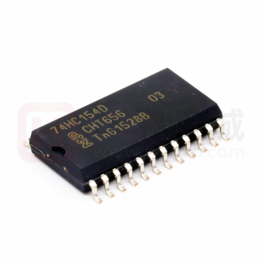
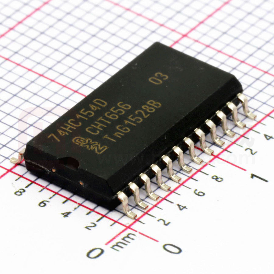
74HC154; 74HCT154
4-to-16 line decoder/demultiplexer
Rev. 06 — 12 February 2007 Product data sheet
1. General description
The 74HC154; 74HCT154 is a high-speed Si-gate CMOS device and is pin compatible with Low-power Schottky TTL (LSTTL). The 74HC154; 74HCT154 decoders accept four active HIGH binary address inputs and provide 16 mutually-exclusive active LOW outputs. The two-input enable gate can be used to strobe the decoder to eliminate the normal decoding ‘glitches’ on the outputs, or can be used for the expansion of the decoder. The enable gate has two ANDed inputs which must be LOW to enable the outputs. The 74HC154; 74HCT154 can be used as a 1-to-16 demultiplexer by using one of the enable inputs as the multiplexed data input. When the other enable input is LOW, the addressed output will follow the state of the applied data.
2. Features
I I I I I 16-line demultiplexing capability Decodes 4 binary-coded inputs into 16 mutually-exclusive outputs Complies with JEDEC standard no. 7A Specified from −40 °C to +85 °C and −40 °C to +125 °C ESD protection: N HBM EIA/JESD22-A114D exceeds 2000 V N MM EIA/JESD22-A115-A exceeds 200 V
3. Ordering information
Table 1. Ordering information Package Temperature range Name 74HC154 74HC154N 74HC154D 74HC154DB 74HC154PW −40 °C to +125 °C −40 °C to +125 °C −40 °C to +125 °C −40 °C to +125 °C DIP24 SO24 SSOP24 TSSOP24 plastic dual in-line package; 24 leads (600 mil) plastic small outline package; 24 leads; body width 7.5 mm SOT101-1 SOT137-1 Description Version Type number
plastic shrink small outline package; 24 leads; body width SOT340-1 5.3 mm plastic thin shrink small outline package; 24 leads; body width 4.4 mm SOT355-1
�NXP Semiconductors
74HC154; 74HCT154
4-to-16 line decoder/demultiplexer
Table 1.
Ordering information …continued Package Temperature range Name Description Version −40 °C to +125 °C DHVQFN24 plastic dual in-line compatible thermal enhanced very thin SOT815-1 quad flat package; no leads; 24 terminals; body 3.5 × 5.5 × 0.85 mm DIP24 SO24 SSOP24 TSSOP24 plastic dual in-line package; 24 leads (600 mil) plastic small outline package; 24 leads; body width 7.5 mm SOT101-1 SOT137-1
Type number 74HC154BQ
74HCT154 74HCT154N 74HCT154D −40 °C to +125 °C −40 °C to +125 °C
74HCT154DB −40 °C to +125 °C 74HCT154PW −40 °C to +125 °C 74HCT154BQ −40 °C to +125 °C
plastic shrink small outline package; 24 leads; body width SOT340-1 5.3 mm plastic thin shrink small outline package; 24 leads; body width 4.4 mm SOT355-1
DHVQFN24 plastic dual in-line compatible thermal enhanced very thin SOT815-1 quad flat package; no leads; 24 terminals; body 3.5 × 5.5 × 0.85 mm
4. Functional diagram
23 22 21 20
A0
A1
A2
A3
18 19
E0 DECODER E1
Y0
Y1
Y2
Y3
Y4
Y5
Y6
Y7
Y8
Y9
Y10 Y11 Y12 Y13 Y14 Y15
1
2
3
4
5
6
7
8
9
10
11
13
14
15
16
17
001aab071
Fig 1. Functional diagram
74HC_HCT154_6
© NXP B.V. 2007. All rights reserved.
Product data sheet
Rev. 06 — 12 February 2007
2 of 21
�NXP Semiconductors
74HC154; 74HCT154
4-to-16 line decoder/demultiplexer
DX 23 22 G 21 20 3 0 0 15 0 1 2 3 4 5 6 7 23 A0 Y0 Y1 22 A1 1 2 8 9 10 11 12 20 18 19 E0 E1 A3 Y14 Y15 16 17 & 18 19 EN 14 15 16 17 18 19 13 1 2 3 4 5 6 7 8 9 10 11 13 14 15 & 23 22 21 20 1 2 4 8
X/Y 0 1 2 3 4 5 6 7 8 9 10 11 12 13 EN 14 15 1 2 3 4 5 6 7 8 9 10 11 13 14 15 16 17
21
A2
001aab069
001aab070
Fig 2. Logic symbol
Fig 3. IEC logic symbol
E0
E1
A0
A1
A2
A3
Y0
Y1
Y2
Y3
Y4
Y5
Y6
Y7
Y8
Y9
Y10
Y11
Y12
Y13
Y14
Y15
001aab072
Fig 4. Logic diagram
74HC_HCT154_6
© NXP B.V. 2007. All rights reserved.
Product data sheet
Rev. 06 — 12 February 2007
3 of 21
�NXP Semiconductors
74HC154; 74HCT154
4-to-16 line decoder/demultiplexer
5. Pinning information
5.1 Pinning
74HC154BQ 74HCT154BQ
terminal 1 index area Y1 Y0 Y1 Y2 Y3 Y4 Y5 Y6 Y7 Y8 1 2 3 4 5 6 7 8 9 24 VCC 23 A0 22 A1 Y2 Y3 Y4 Y5 Y6 Y7 Y8 2 3 4 5 6 7 8 9 VCC(1) GND 12 Y11 13 24 VCC 23 A0 22 A1 21 A2 20 A3 19 E1 18 E0 17 Y15 16 Y14 15 Y13 14 Y12 Y0 1
74HC154D 74HCT154D 74HC154DB 74HCT154DB 74HC154N 74HCT154N 74HC154PW 74HCT154PW
21 A2 20 A3 19 E1 18 E0 17 Y15 16 Y14 15 Y13 14 Y12 13 Y11
Y9 10 Y10 11
Y9 10 Y10 11 GND 12
001aab067
001aab068
Transparent top view
(1) The die substrate is attached to this pad using conductive die attach material. It cannot be used as a supply pin or input.
Fig 5. Pin configuration for SO24, DIP24, SSOP24 and TSSOP24
Fig 6. Pin configuration for DHVQFN24
5.2 Pin description
Table 2. Symbol Y0 Y1 Y2 Y3 Y4 Y5 Y6 Y7 Y8 Y9 Y10 GND Y11 Y12
74HC_HCT154_6
Pin description Pin 1 2 3 4 5 6 7 8 9 10 11 12 13 14 Description data output (active LOW) data output (active LOW) data output (active LOW) data output (active LOW) data output (active LOW) data output (active LOW) data output (active LOW) data output (active LOW) data output (active LOW) data output (active LOW) data output (active LOW) ground (0 V) data output (active LOW) data output (active LOW)
© NXP B.V. 2007. All rights reserved.
Product data sheet
Rev. 06 — 12 February 2007
4 of 21
�NXP Semiconductors
74HC154; 74HCT154
4-to-16 line decoder/demultiplexer
Table 2. Symbol Y13 Y14 Y15 E0 E1 A3 A2 A1 A0 VCC
Pin description …continued Pin 15 16 17 18 19 20 21 22 23 24 Description data output (active LOW) data output (active LOW) data output (active LOW) enable input (active LOW) enable input (active LOW) address input address input address input address input supply voltage
6. Functional description
Table 3. Input H H L L H L H L X X X L H L H L H L H L H L H L H L H
[1]
Function table[1] Output Y6 H H H H H H H H H L H H H H H H H H H Y7 H H H H H H H H H H L H H H H H H H H Y8 H H H H H H H H H H H L H H H H H H H Y9 H H H H H H H H H H H H L H H H H H H Y10 Y11 Y12 Y13 Y14 Y15 H H H H H H H H H H H H H L H H H H H H H H H H H H H H H H H H H L H H H H H H H H H H H H H H H H H H H L H H H H H H H H H H H H H H H H H H H L H H H H H H H H H H H H H H H H H H H L H H H H H H H H H H H H H H H H H H H L X X X L L H H L L H H L L H H L L H H X X X L L L L H H H H L L L L H H H H X X X L L L L L L L L H H H H H H H H H H H L H H H H H H H H H H H H H H H H H H H L H H H H H H H H H H H H H H H H H H H L H H H H H H H H H H H H H H H H H H H L H H H H H H H H H H H H H H H H H H H L H H H H H H H H H H H H H H H H H H H L H H H H H H H H H H
E0 E1 A0 A1 A2 A3 Y0 Y1 Y2 Y3 Y4 Y5
H = HIGH voltage level L = LOW voltage level X = don’t care.
74HC_HCT154_6
© NXP B.V. 2007. All rights reserved.
Product data sheet
Rev. 06 — 12 February 2007
5 of 21
�NXP Semiconductors
74HC154; 74HCT154
4-to-16 line decoder/demultiplexer
7. Limiting values
Table 4. Limiting values In accordance with the Absolute Maximum Rating System (IEC 60134). Voltages are referenced to GND (ground = 0 V). Symbol VCC IIK IOK IO ICC IGND Tstg Ptot
[1] [2]
Parameter supply voltage input clamping current output clamping current output current supply current ground current storage temperature total power dissipation
Conditions VI < −0.5 V or VI > VCC + 0.5 V VO < −0.5 V or VO > VCC + 0.5 V −0.5 V < VO < VCC + 0.5 V
[1] [1] [1] [1] [1]
Min −0.5 −65 -
Max +7.0 ±20 ±20 ±25 50 −50 +150 300
Unit V mA mA mA mA mA °C mW
Tamb = −40 °C to +125 °C
[2]
The input and output voltage ratings may be exceeded if the input and output current ratings are observed. For DIP24 packages: Ptot derates linearly at 12 mW/K above 70 °C. For SO24 packages: Ptot derates linearly at 8 mW/K above 70 °C. For SSOP24 and TSSOP24 packages: Ptot derates linearly at 5.5 mW/K above 60 °C. For DHVQFN24 packages: Ptot derates linearly at 4.5 mW/K above 60 °C.
8. Recommended operating conditions
Table 5. Symbol 74HC154 VCC VI VO Tamb tr supply voltage input voltage output voltage ambient temperature rise time VCC = 2.0 V VCC = 4.5 V VCC = 6.0 V tf fall time VCC = 2.0 V VCC = 4.5 V VCC = 6.0 V 74HCT154 VCC VI VO Tamb tr tf supply voltage input voltage output voltage ambient temperature input rise time input fall time VCC = 4.5 V VCC = 4.5 V 4.5 0 0 −40 5.0 +25 6.0 6.0 5.5 VCC VCC +125 500 500 V V V °C ns ns 2.0 0 0 −40 5.0 +25 6.0 6.0 6.0 VCC VCC +125 1000 500 400 1000 500 400 V V V °C ns ns ns ns ns ns Operating conditions Parameter Conditions Min Typ Max Unit
74HC_HCT154_6
© NXP B.V. 2007. All rights reserved.
Product data sheet
Rev. 06 — 12 February 2007
6 of 21
�NXP Semiconductors
74HC154; 74HCT154
4-to-16 line decoder/demultiplexer
9. Static characteristics
Table 6. Static characteristics 74HC154 At recommended operating conditions; voltages are referenced to GND (ground = 0 V). Symbol Tamb = 25 °C VIH HIGH-level input voltage VCC = 2.0 V VCC = 4.5 V VCC = 6.0 V VIL LOW-level input voltage VCC = 2.0 V VCC = 4.5 V VCC = 6.0 V VOH HIGH-level output voltage VI = VIH or VIL VCC = 2.0 V; IO = −20 µA VCC = 4.5 V; IO = −20 µA VCC = 6.0 V; IO = −20 µA VCC = 4.5 V; IO = −4.0 mA VCC = 6.0 V; IO = −5.2 mA VOL LOW-level output voltage VI = VIH or VIL VCC = 2.0 V; IO = 20 µA VCC = 4.5 V; IO = 20 µA VCC = 6.0 V; IO = 20 µA VCC = 4.5 V; IO = 4.0 mA VCC = 6.0 V; IO = 5.2 mA II ICC CI VIH input leakage current supply current input capacitance HIGH-level input voltage VCC = 2.0 V VCC = 4.5 V VCC = 6.0 V VIL LOW-level input voltage VCC = 2.0 V VCC = 4.5 V VCC = 6.0 V VOH HIGH-level output voltage VI = VIH or VIL VCC = 2.0 V; IO = −20 µA VCC = 4.5 V; IO = −20 µA VCC = 6.0 V; IO = −20 µA VCC = 4.5 V; IO = −4.0 mA VCC = 6.0 V; IO = −5.2 mA 1.9 4.4 5.9 3.84 5.34 V V V V V VCC = 6.0 V; VI = VCC or GND VCC = 6.0 V; VI = VCC or GND; IO = 0 A 1.5 3.15 4.2 0 0 0 0.15 0.16 3.5 0.1 0.1 0.1 0.26 0.26 ±0.1 8.0 0.5 1.35 1.8 V V V V V µA µA pF V V V V V V 1.9 4.4 5.9 3.98 5.48 2.0 4.5 6.0 4.32 5.81 V V V V V 1.5 3.15 4.2 1.2 2.4 3.2 0.8 2.1 2.8 0.5 1.35 1.8 V V V V V V Parameter Conditions Min Typ Max Unit
Tamb = −40 °C to +85 °C
74HC_HCT154_6
© NXP B.V. 2007. All rights reserved.
Product data sheet
Rev. 06 — 12 February 2007
7 of 21
�NXP Semiconductors
74HC154; 74HCT154
4-to-16 line decoder/demultiplexer
Table 6. Static characteristics 74HC154 …continued At recommended operating conditions; voltages are referenced to GND (ground = 0 V). Symbol VOL Parameter LOW-level output voltage Conditions VI = VIH or VIL VCC = 2.0 V; IO = 20 µA VCC = 4.5 V; IO = 20 µA VCC = 6.0 V; IO = 20 µA VCC = 4.5 V; IO = 4.0 mA VCC = 6.0 V; IO = 5.2 mA II ICC VIH input leakage current supply current HIGH-level input voltage VCC = 6.0 V; VI = VCC or GND VCC = 6.0 V; VI = VCC or GND; IO = 0 A VCC = 2.0 V VCC = 4.5 V VCC = 6.0 V VIL LOW-level input voltage VCC = 2.0 V VCC = 4.5 V VCC = 6.0 V VOH HIGH-level output voltage VI = VIH or VIL VCC = 2.0 V; IO = −20 µA VCC = 4.5 V; IO = −20 µA VCC = 6.0 V; IO = −20 µA VCC = 4.5 V; IO = −4.0 mA VCC = 6.0 V; IO = −5.2 mA VOL LOW-level output voltage VI = VIH or VIL VCC = 2.0 V; IO = 20 µA VCC = 4.5 V; IO = 20 µA VCC = 6.0 V; IO = 20 µA VCC = 4.5 V; IO = 4.0 mA VCC = 6.0 V; IO = 5.2 mA II ICC input leakage current supply current VCC = 6.0 V; VI = VCC or GND VCC = 6.0 V; VI = VCC or GND; IO = 0 A 0.1 0.1 0.1 0.4 0.4 ±0.1 160 V V V V V µA µA 1.9 4.4 5.9 3.7 5.2 V V V V V 1.5 3.15 4.2 0.1 0.1 0.1 0.33 0.33 ±1.0 80 0.5 1.35 1.8 V V V V V µA µA V V V V V V Min Typ Max Unit
Tamb = −40 °C to +125 °C
Table 7. Static characteristics 74HCT154 At recommended operating conditions; voltages are referenced to GND (ground = 0 V). Symbol Tamb = 25 °C VIH VIL VOH HIGH-level input voltage LOW-level input voltage HIGH-level output voltage VCC = 4.5 V to 5.5 V VCC = 4.5 V to 5.5 V VI = VIH or VIL VCC = 4.5 V; IO = −20 µA VCC = 4.5 V; IO = −4 mA 4.4 3.98 4.5 4.32 V V 2.0 1.6 1.2 0.8 V V Parameter Conditions Min Typ Max Unit
74HC_HCT154_6
© NXP B.V. 2007. All rights reserved.
Product data sheet
Rev. 06 — 12 February 2007
8 of 21
�NXP Semiconductors
74HC154; 74HCT154
4-to-16 line decoder/demultiplexer
Table 7. Static characteristics 74HCT154 …continued At recommended operating conditions; voltages are referenced to GND (ground = 0 V). Symbol VOL Parameter LOW-level output voltage Conditions VI = VIH or VIL VCC = 4.5 V; IO = 20 µA VCC = 4.5 V; IO = 4 mA II ICC ∆ICC CI VIH VIL VOH input leakage current supply current additional supply current input capacitance HIGH-level input voltage LOW-level input voltage HIGH-level output voltage VCC = 4.5 V to 5.5 V VCC = 4.5 V to 5.5 V VI = VIH or VIL VCC = 4.5 V; IO = −20 µA VCC = 4.5 V; IO = −4 mA VOL LOW-level output voltage VI = VIH or VIL VCC = 4.5 V; IO = 20 µA VCC = 4.5 V; IO = 4 mA II ICC ∆ICC input leakage current supply current additional supply current VCC = 5.5 V; VI = VCC or GND VCC = 5.5 V; VI = VCC or GND; IO = 0 A per input pin; VCC = 4.5 V to 5.5 V; VI = VCC − 2.1 V; IO = 0 A VCC = 4.5 V to 5.5 V VCC = 4.5 V to 5.5 V VI = VIH or VIL VCC = 4.5 V; IO = −20 µA VCC = 4.5 V; IO = −4 mA VOL LOW-level output voltage VI = VIH or VIL VCC = 4.5 V; IO = 20 µA VCC = 4.5 V; IO = 4 mA II ICC ∆ICC input leakage current supply current additional supply current VCC = 5.5 V; VI = VCC or GND VCC = 5.5 V; VI = VCC or GND; IO = 0 A per input pin; VCC = 4.5 V to 5.5 V; VI = VCC − 2.1 V; IO = 0 A 0.1 0.4 ±1.0 160 490 V V µA µA µA 4.4 3.7 V V 0.1 0.33 ±1.0 80 450 V V µA µA µA 4.4 3.84 V V VCC = 5.5 V; VI = VCC or GND VCC = 5.5 V; VI = VCC or GND; IO = 0 A per input pin; VCC = 4.5 V to 5.5 V; VI = VCC − 2.1 V; IO = 0 A 2.0 0 0.15 3.5 0.1 0.25 ±0.1 8.0 360 0.8 V V µA µA µA pF V V Min Typ Max Unit
Tamb = −40 °C to +85 °C
Tamb = −40 °C to +125 °C VIH VIL VOH HIGH-level input voltage LOW-level input voltage HIGH-level output voltage 2.0 0.8 V V
74HC_HCT154_6
© NXP B.V. 2007. All rights reserved.
Product data sheet
Rev. 06 — 12 February 2007
9 of 21
�NXP Semiconductors
74HC154; 74HCT154
4-to-16 line decoder/demultiplexer
10. Dynamic characteristics
Table 8. Dynamic characteristics GND (ground = 0 V); CL = 50 pF unless otherwise specified; for test circuit, see Figure 9. Symbol Parameter Conditions Min 74HC154 tpd propagation delay An to Yn; see Figure 7 VCC = 2.0 V VCC = 4.5 V VCC = 5 V; CL = 15 pF VCC = 6.0 V En to Yn; see Figure 8 VCC = 2.0 V VCC = 4.5 V VCC = 5 V; CL = 15 pF VCC = 6.0 V tt transition time see Figure 7 and 8 VCC = 2.0 V VCC = 4.5 V VCC = 6.0 V CPD 74HCT154 tpd propagation delay An to Yn; see Figure 7 VCC = 4.5 V VCC = 5 V; CL = 15 pF En to Yn; see Figure 8 VCC = 4.5 V VCC = 5 V; CL = 15 pF tt CPD transition time power dissipation capacitance
tpd is the same as tPLH and tPHL tt is the same as tTLH and tTHL CPD is used to determine the dynamic power dissipation (PD in µW). PD = CPD × VCC2 × fi × N + Σ(CL × VCC2 × fo) where: fi = input frequency in MHz; fo = output frequency in MHz; CL = output load capacitance in pF; VCC = supply voltage in V; N = number of load switching outputs; Σ(CL × VCC2 × fo) = sum of the outputs.
© NXP B.V. 2007. All rights reserved.
25 °C Typ Max
−40 °C to +125 °C Min Max (85 °C) Max (125 °C)
Unit
[1]
[2]
36 13 11 10 39 14 11 11 19 7 6 60
150 30 26 150 30 26 75 15 13 -
-
190 38 33 190 38 33 95 19 16 -
225 45 38 225 45 38 110 22 19 -
ns ns ns ns ns ns ns ns ns ns ns pF
[3]
power dissipation capacitance
per gate; VI = GND to VCC
-
[1]
[2]
16 13 15 13 7 60
35 32 15 -
-
44 40 19 -
53 48 22 -
ns ns ns ns ns pF
see Figure 7 and 8 VCC = 4.5 V per gate; VI = GND to (VCC − 1.5 V)
[3]
-
[1] [2] [3]
74HC_HCT154_6
Product data sheet
Rev. 06 — 12 February 2007
10 of 21
�NXP Semiconductors
74HC154; 74HCT154
4-to-16 line decoder/demultiplexer
11. Waveforms
VI An input GND t PHL VOH Yn output VOL t THL 90 % VM 10 % VM 10 % t TLH
001aab073
VI VM VM En input GND t PLH 90 % VOH Yn output VOL 90 % VM 10 % t THL VM 10 % t TLH
001aab074
VM
VM
tPHL
tPLH 90 %
Measurement points are given in Table 9.
Measurement points are given in Table 9.
Fig 7. Propagation delay address input (An) to output (Yn) and transition time output (Yn) Table 9. Type 74HC154 74HCT154 Measurement points Input VM 0.5VCC 1.3 V
Fig 8. Propagation delay enable input (En) to output (Yn) and transition time output (Yn)
Output VM 0.5VCC 1.3 V
74HC_HCT154_6
© NXP B.V. 2007. All rights reserved.
Product data sheet
Rev. 06 — 12 February 2007
11 of 21
�NXP Semiconductors
74HC154; 74HCT154
4-to-16 line decoder/demultiplexer
VI negative pulse 0V
tW 90 % VM 10 % tf tr tr tf 90 % VM 10 % tW VM VM
VI positive pulse 0V
VCC
VCC
PULSE GENERATOR
VI
VO
RL
S1
DUT
RT CL
open
001aad983
Test data is given in Table 10. Definitions for test circuit: RT = Termination resistance; should be equal to output impedance Zo of the pulse generator. CL = Load capacitance including jig and probe capacitance. RL = Load resistor. S1 = Test selection switch.
Fig 9. Load circuitry for measuring switching times Table 10. Type 74HC154 74HCT154 Test data Input VI VCC 3V tr, tf 6 ns 6 ns Load CL 15 pF, 50 pF 15 pF, 50 pF RL 1 kΩ 1 kΩ S1 position tPHL, tPLH open open
74HC_HCT154_6
© NXP B.V. 2007. All rights reserved.
Product data sheet
Rev. 06 — 12 February 2007
12 of 21
�NXP Semiconductors
74HC154; 74HCT154
4-to-16 line decoder/demultiplexer
12. Application information
A0 A1 A2 A3
Y0 Y1
A0 A1 A2 A3
Y0 Y1
strobe
E0 E1
Y14 Y15
001aab075
data input
E0 E1
Y14 Y15
001aab076
Fig 10. 1-of-16 decoder; LOW level output selected
Fig 11. 1-of-16 demultiplexer; logic level on selected outputs follow the logic level on the data input
74HC_HCT154_6
© NXP B.V. 2007. All rights reserved.
Product data sheet
Rev. 06 — 12 February 2007
13 of 21
�NXP Semiconductors
74HC154; 74HCT154
4-to-16 line decoder/demultiplexer
13. Package outline
DIP24: plastic dual in-line package; 24 leads (600 mil) SOT101-1
seating plane
D
ME
A2
A
L
A1 c Z e b1 b 24 13 MH wM (e 1)
pin 1 index E
1
12
0
5 scale
10 mm
DIMENSIONS (inch dimensions are derived from the original mm dimensions) UNIT mm inches A max. 5.1 0.2 A1 min. 0.51 0.02 A2 max. 4 0.16 b 1.7 1.3 0.066 0.051 b1 0.53 0.38 0.021 0.015 c 0.32 0.23 0.013 0.009 D (1) 32.0 31.4 1.26 1.24 E (1) 14.1 13.7 0.56 0.54 e 2.54 0.1 e1 15.24 0.6 L 3.9 3.4 0.15 0.13 ME 15.80 15.24 0.62 0.60 MH 17.15 15.90 0.68 0.63 w 0.25 0.01 Z (1) max. 2.2 0.087
Note 1. Plastic or metal protrusions of 0.25 mm (0.01 inch) maximum per side are not included. OUTLINE VERSION SOT101-1 REFERENCES IEC 051G02 JEDEC MO-015 JEITA SC-509-24 EUROPEAN PROJECTION
ISSUE DATE 99-12-27 03-02-13
Fig 12. Package outline SOT101-1 (DIP24)
74HC_HCT154_6 © NXP B.V. 2007. All rights reserved.
Product data sheet
Rev. 06 — 12 February 2007
14 of 21
�NXP Semiconductors
74HC154; 74HCT154
4-to-16 line decoder/demultiplexer
SO24: plastic small outline package; 24 leads; body width 7.5 mm
SOT137-1
D
E
A X
c y HE vMA
Z 24 13
Q A2 A1 pin 1 index Lp L 1 e bp 12 wM detail X (A 3) θ A
0
5 scale
10 mm
DIMENSIONS (inch dimensions are derived from the original mm dimensions) UNIT mm inches A max. 2.65 0.1 A1 0.3 0.1 A2 2.45 2.25 A3 0.25 0.01 bp 0.49 0.36 c 0.32 0.23 D (1) 15.6 15.2 0.61 0.60 E (1) 7.6 7.4 0.30 0.29 e 1.27 0.05 HE 10.65 10.00 L 1.4 Lp 1.1 0.4 Q 1.1 1.0 0.043 0.039 v 0.25 0.01 w 0.25 0.01 y 0.1 Z
(1)
θ
0.9 0.4
0.012 0.096 0.004 0.089
0.019 0.013 0.014 0.009
0.419 0.043 0.055 0.394 0.016
0.035 0.004 0.016
8 o 0
o
Note 1. Plastic or metal protrusions of 0.15 mm (0.006 inch) maximum per side are not included. OUTLINE VERSION SOT137-1 REFERENCES IEC 075E05 JEDEC MS-013 JEITA EUROPEAN PROJECTION
ISSUE DATE 99-12-27 03-02-19
Fig 13. Package outline SOT137-1 (SO24)
74HC_HCT154_6 © NXP B.V. 2007. All rights reserved.
Product data sheet
Rev. 06 — 12 February 2007
15 of 21
�NXP Semiconductors
74HC154; 74HCT154
4-to-16 line decoder/demultiplexer
SSOP24: plastic shrink small outline package; 24 leads; body width 5.3 mm
SOT340-1
D
E
A X
c y HE vMA
Z 24 13
Q A2 pin 1 index A1 (A 3) θ Lp L 1 e bp 12 wM detail X A
0
2.5 scale
5 mm
DIMENSIONS (mm are the original dimensions) UNIT mm A max. 2 A1 0.21 0.05 A2 1.80 1.65 A3 0.25 bp 0.38 0.25 c 0.20 0.09 D (1) 8.4 8.0 E (1) 5.4 5.2 e 0.65 HE 7.9 7.6 L 1.25 Lp 1.03 0.63 Q 0.9 0.7 v 0.2 w 0.13 y 0.1 Z (1) 0.8 0.4 θ 8 o 0
o
Note 1. Plastic or metal protrusions of 0.2 mm maximum per side are not included. OUTLINE VERSION SOT340-1 REFERENCES IEC JEDEC MO-150 JEITA EUROPEAN PROJECTION
ISSUE DATE 99-12-27 03-02-19
Fig 14. Package outline SOT340-1 (SSOP24)
74HC_HCT154_6 © NXP B.V. 2007. All rights reserved.
Product data sheet
Rev. 06 — 12 February 2007
16 of 21
�NXP Semiconductors
74HC154; 74HCT154
4-to-16 line decoder/demultiplexer
TSSOP24: plastic thin shrink small outline package; 24 leads; body width 4.4 mm
SOT355-1
D
E
A
X
c y HE vMA
Z
24
13
Q A2 pin 1 index A1 (A 3) A
θ Lp L
1
e bp
12
wM detail X
0
2.5 scale
5 mm
DIMENSIONS (mm are the original dimensions) UNIT mm A max. 1.1 A1 0.15 0.05 A2 0.95 0.80 A3 0.25 bp 0.30 0.19 c 0.2 0.1 D (1) 7.9 7.7 E (2) 4.5 4.3 e 0.65 HE 6.6 6.2 L 1 Lp 0.75 0.50 Q 0.4 0.3 v 0.2 w 0.13 y 0.1 Z (1) 0.5 0.2 θ 8o 0o
Notes 1. Plastic or metal protrusions of 0.15 mm maximum per side are not included. 2. Plastic interlead protrusions of 0.25 mm maximum per side are not included. OUTLINE VERSION SOT355-1 REFERENCES IEC JEDEC MO-153 JEITA EUROPEAN PROJECTION ISSUE DATE 99-12-27 03-02-19
Fig 15. Package outline SOT355-1 (TSSOP24)
74HC_HCT154_6 © NXP B.V. 2007. All rights reserved.
Product data sheet
Rev. 06 — 12 February 2007
17 of 21
�NXP Semiconductors
74HC154; 74HCT154
4-to-16 line decoder/demultiplexer
DHVQFN24: plastic dual in-line compatible thermal enhanced very thin quad flat package; no leads; 24 terminals; body 3.5 x 5.5 x 0.85 mm
SOT815-1
D
B
A
E
A
A1 c
detail X terminal 1 index area C terminal 1 index area 2 L 12 e1 e b 11 vMCAB wM C y1 C y
1
Eh
e2
24 13
23 Dh 0
14 X 2.5 scale 5 mm
DIMENSIONS (mm are the original dimensions) UNIT mm A(1) max. 1 A1 0.05 0.00 b 0.30 0.18 c 0.2 D (1) 5.6 5.4 Dh 4.25 3.95 E (1) 3.6 3.4 Eh 2.25 1.95 e 0.5 e1 4.5 e2 1.5 L 0.5 0.3 v 0.1 w 0.05 y 0.05 y1 0.1
Note 1. Plastic or metal protrusions of 0.075 mm maximum per side are not included. OUTLINE VERSION SOT815-1 REFERENCES IEC --JEDEC --JEITA --EUROPEAN PROJECTION
ISSUE DATE 03-04-29
Fig 16. Package outline SOT815-1 (DHVQFN24)
74HC_HCT154_6 © NXP B.V. 2007. All rights reserved.
Product data sheet
Rev. 06 — 12 February 2007
18 of 21
�NXP Semiconductors
74HC154; 74HCT154
4-to-16 line decoder/demultiplexer
14. Abbreviations
Table 11. Acronym CMOS DUT ESD HBM LSTTL MM Abbreviations Description Complementary Metal Oxide Semiconductor Device Under Test ElectroStatic Discharge Human Body Model Low-power Schottky Transistor-Transistor Logic Machine Model
15. Revision history
Table 12. Revision history Release date 20070212 Data sheet status Product data sheet Change notice Supersedes 74HC_HCT154_5 Document ID 74HC_HCT154_6 Modifications:
• • •
The format of this data sheet has been redesigned to comply with the new identity guidelines of NXP Semiconductors. Legal texts have been adapted to the new company name where appropriate. Table 3 on page 5: Corrected errors in output information. Product specification Product specification Product specification 74HC_HCT154_4 74HC_HCT154_3 74HC_HCT154_CNV_2
74HC_HCT154_5 74HC_HCT154_4 74HC_HCT154_3
20041012 20041005 20040601
74HC_HCT154_6
© NXP B.V. 2007. All rights reserved.
Product data sheet
Rev. 06 — 12 February 2007
19 of 21
�NXP Semiconductors
74HC154; 74HCT154
4-to-16 line decoder/demultiplexer
16. Legal information
16.1 Data sheet status
Document status[1][2] Objective [short] data sheet Preliminary [short] data sheet Product [short] data sheet
[1] [2] [3]
Product status[3] Development Qualification Production
Definition This document contains data from the objective specification for product development. This document contains data from the preliminary specification. This document contains the product specification.
Please consult the most recently issued document before initiating or completing a design. The term ‘short data sheet’ is explained in section “Definitions”. The product status of device(s) described in this document may have changed since this document was published and may differ in case of multiple devices. The latest product status information is available on the Internet at URL http://www.nxp.com.
16.2 Definitions
Draft — The document is a draft version only. The content is still under internal review and subject to formal approval, which may result in modifications or additions. NXP Semiconductors does not give any representations or warranties as to the accuracy or completeness of information included herein and shall have no liability for the consequences of use of such information. Short data sheet — A short data sheet is an extract from a full data sheet with the same product type number(s) and title. A short data sheet is intended for quick reference only and should not be relied upon to contain detailed and full information. For detailed and full information see the relevant full data sheet, which is available on request via the local NXP Semiconductors sales office. In case of any inconsistency or conflict with the short data sheet, the full data sheet shall prevail.
malfunction of a NXP Semiconductors product can reasonably be expected to result in personal injury, death or severe property or environmental damage. NXP Semiconductors accepts no liability for inclusion and/or use of NXP Semiconductors products in such equipment or applications and therefore such inclusion and/or use is at the customer’s own risk. Applications — Applications that are described herein for any of these products are for illustrative purposes only. NXP Semiconductors makes no representation or warranty that such applications will be suitable for the specified use without further testing or modification. Limiting values — Stress above one or more limiting values (as defined in the Absolute Maximum Ratings System of IEC 60134) may cause permanent damage to the device. Limiting values are stress ratings only and operation of the device at these or any other conditions above those given in the Characteristics sections of this document is not implied. Exposure to limiting values for extended periods may affect device reliability. Terms and conditions of sale — NXP Semiconductors products are sold subject to the general terms and conditions of commercial sale, as published at http://www.nxp.com/profile/terms, including those pertaining to warranty, intellectual property rights infringement and limitation of liability, unless explicitly otherwise agreed to in writing by NXP Semiconductors. In case of any inconsistency or conflict between information in this document and such terms and conditions, the latter will prevail. No offer to sell or license — Nothing in this document may be interpreted or construed as an offer to sell products that is open for acceptance or the grant, conveyance or implication of any license under any copyrights, patents or other industrial or intellectual property rights.
16.3 Disclaimers
General — Information in this document is believed to be accurate and reliable. However, NXP Semiconductors does not give any representations or warranties, expressed or implied, as to the accuracy or completeness of such information and shall have no liability for the consequences of use of such information. Right to make changes — NXP Semiconductors reserves the right to make changes to information published in this document, including without limitation specifications and product descriptions, at any time and without notice. This document supersedes and replaces all information supplied prior to the publication hereof. Suitability for use — NXP Semiconductors products are not designed, authorized or warranted to be suitable for use in medical, military, aircraft, space or life support equipment, nor in applications where failure or
16.4 Trademarks
Notice: All referenced brands, product names, service names and trademarks are the property of their respective owners.
17. Contact information
For additional information, please visit: http://www.nxp.com For sales office addresses, send an email to: salesaddresses@nxp.com
74HC_HCT154_6
© NXP B.V. 2007. All rights reserved.
Product data sheet
Rev. 06 — 12 February 2007
20 of 21
�NXP Semiconductors
74HC154; 74HCT154
4-to-16 line decoder/demultiplexer
18. Contents
1 2 3 4 5 5.1 5.2 6 7 8 9 10 11 12 13 14 15 16 16.1 16.2 16.3 16.4 17 18 General description . . . . . . . . . . . . . . . . . . . . . . 1 Features . . . . . . . . . . . . . . . . . . . . . . . . . . . . . . . 1 Ordering information . . . . . . . . . . . . . . . . . . . . . 1 Functional diagram . . . . . . . . . . . . . . . . . . . . . . 2 Pinning information . . . . . . . . . . . . . . . . . . . . . . 4 Pinning . . . . . . . . . . . . . . . . . . . . . . . . . . . . . . . 4 Pin description . . . . . . . . . . . . . . . . . . . . . . . . . 4 Functional description . . . . . . . . . . . . . . . . . . . 5 Limiting values. . . . . . . . . . . . . . . . . . . . . . . . . . 6 Recommended operating conditions. . . . . . . . 6 Static characteristics. . . . . . . . . . . . . . . . . . . . . 7 Dynamic characteristics . . . . . . . . . . . . . . . . . 10 Waveforms . . . . . . . . . . . . . . . . . . . . . . . . . . . . 11 Application information. . . . . . . . . . . . . . . . . . 13 Package outline . . . . . . . . . . . . . . . . . . . . . . . . 14 Abbreviations . . . . . . . . . . . . . . . . . . . . . . . . . . 19 Revision history . . . . . . . . . . . . . . . . . . . . . . . . 19 Legal information. . . . . . . . . . . . . . . . . . . . . . . 20 Data sheet status . . . . . . . . . . . . . . . . . . . . . . 20 Definitions . . . . . . . . . . . . . . . . . . . . . . . . . . . . 20 Disclaimers . . . . . . . . . . . . . . . . . . . . . . . . . . . 20 Trademarks . . . . . . . . . . . . . . . . . . . . . . . . . . . 20 Contact information. . . . . . . . . . . . . . . . . . . . . 20 Contents . . . . . . . . . . . . . . . . . . . . . . . . . . . . . . 21
Please be aware that important notices concerning this document and the product(s) described herein, have been included in section ‘Legal information’.
© NXP B.V. 2007.
All rights reserved.
For more information, please visit: http://www.nxp.com For sales office addresses, please send an email to: salesaddresses@nxp.com Date of release: 12 February 2007 Document identifier: 74HC_HCT154_6
�
很抱歉,暂时无法提供与“74HC154D”相匹配的价格&库存,您可以联系我们找货
免费人工找货- 国内价格
- 1+1.98643
- 30+1.91793
- 100+1.78094
- 500+1.64394
- 1000+1.57545


 工商网监
湘ICP备2023018690号
工商网监
湘ICP备2023018690号
