NXP Semiconductors
Technical Data
Document Number: AFIC31025N
Rev. 0, 10/2017
RF LDMOS Integrated
Power Amplifiers
AFIC31025N
AFIC31025GN
The AFIC31025N integrated circuit is designed with on--chip matching that
makes it usable from 2400 to 3100 MHz. This multi--stage device is designed
to support CW and pulse applications.
Typical Performance: In 2400–3100 MHz reference circuit, VDD = 32 Vdc
Frequency
(MHz)
Signal Type
Pout
(W)
Gps
(dB)
D
(%)
2400–2500
CW
25
30.0
45.5
2700–3100
Pulse
(300 sec, 15% Duty Cycle)
25 Peak
22.0
40.0
2400–3100 MHz, 25 W PEAK, 32 V
AIRFAST RF LDMOS
INTEGRATED POWER AMPLIFIERS
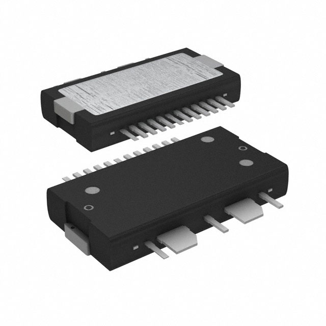
TO--270WB--17
PLASTIC
AFIC31025N
Features
On--chip matching (50 ohm input, DC blocked)
Integrated quiescent current temperature compensation with
enable/disable function (1)
Qualified up to a maximum of 32 VDD operation
Integrated ESD protection
TO--270WBG--17
PLASTIC
AFIC31025GN
Typical Applications
Civil S--Band radar
Weather radar
Maritime radar
Industrial heating
Data links
Plasma generation
VDS1A
VBWA
RFinA
VGS1A
VGS2A
VGS1B
VGS2B
RFout1/VDS2A
Quiescent Current
Temperature Compensation (1)
Quiescent Current
Temperature Compensation (1)
RFinB
RFout2/VDS2B
VDS1B
VBWB
Figure 1. Functional Block Diagram
VDS1A
VGS2A
VGS1A
RFinA
N.C.
GND
GND
N.C.
RFinB
VGS1B
VGS2B
VDS1B
1
2
3
4
5
6
7
8
9
10
11
12
Carrier
17
16
15
14
13
Peaking
VBWA
RFout1/VDS2A
GND
RFout2/VDS2B
VBWB
(Top View)
Note: Exposed backside of the package is
the source terminal for the transistor.
Figure 2. Pin Connections
1. Refer to AN1977, Quiescent Current Thermal Tracking Circuit in the RF Integrated Circuit Family, and to AN1987, Quiescent Current Control
for the RF Integrated Circuit Device Family. Go to http://www.nxp.com/RF and search for AN1977 or AN1987.
2017 NXP B.V.
RF Device Data
NXP Semiconductors
AFIC31025N AFIC31025GN
1
�Table 1. Maximum Ratings
Rating
Symbol
Value
Unit
Drain--Source Voltage
VDSS
–0.5, +65
Vdc
Gate--Source Voltage
VGS
–0.5, +10
Vdc
Operating Voltage
VDD
32, +0
Vdc
Storage Temperature Range
Tstg
–65 to +150
C
Case Operating Temperature Range
TC
–40 to +150
C
Operating Junction Temperature Range (1)
TJ
–40 to +225
C
Input Power
Pin
20
dBm
Symbol
Value (2)
Unit
Table 2. Thermal Characteristics
Characteristic
Thermal Resistance, Junction to Case
Case Temperature 81C, DC, Total PD = 29.3 W
Stage 1, 28 Vdc, PD = 3.8 W
Stage 2, 28 Vdc, PD = 25.5 W
RJC
C/W
5.85
1.92
Table 3. ESD Protection Characteristics
Test Methodology
Class
Human Body Model (per JESD22--A114)
1B
Charge Device Model (per JESD22--C101)
II
Table 4. Moisture Sensitivity Level
Test Methodology
Per JESD22--A113, IPC/JEDEC J--STD--020
Rating
Package Peak Temperature
Unit
3
260
C
Table 5. Electrical Characteristics (TA = 25C unless otherwise noted)
Symbol
Min
Typ
Max
Unit
Zero Gate Voltage Drain Leakage Current
(VDS = 65 Vdc, VGS = 0 Vdc)
IDSS
—
—
10
Adc
Zero Gate Voltage Drain Leakage Current
(VDS = 32 Vdc, VGS = 0 Vdc)
IDSS
—
—
1
Adc
Gate--Source Leakage Current
(VGS = 1.0 Vdc, VDS = 0 Vdc)
IGSS
—
—
1
Adc
Gate Threshold Voltage (3)
(VDS = 10 Vdc, ID = 2.5 Adc)
VGS(th)
0.8
1.2
1.6
Vdc
Gate Quiescent Voltage
(VDS = 28 Vdc, IDQ1(A+B) = 59 mAdc)
VGS(Q)
—
2.0
—
Vdc
Fixture Gate Quiescent Voltage
(VDD = 28 Vdc, IDQ1(A+B) = 59 mAdc, Measured in Functional Test)
VGG(Q)
4.6
5.3
6.1
Vdc
Characteristic
Stage 1 -- Off Characteristics
(3)
Stage 1 -- On Characteristics
1. Continuous use at maximum temperature will affect MTTF.
2. Refer to AN1955, Thermal Measurement Methodology of RF Power Amplifiers. Go to http://www.nxp.com/RF and search for AN1955.
3. Each side of device measured separately.
(continued)
AFIC31025N AFIC31025GN
2
RF Device Data
NXP Semiconductors
�Table 5. Electrical Characteristics (TA = 25C unless otherwise noted) (continued)
Characteristic
Symbol
Min
Typ
Max
Unit
Zero Gate Voltage Drain Leakage Current
(VDS = 65 Vdc, VGS = 0 Vdc)
IDSS
—
—
10
Adc
Zero Gate Voltage Drain Leakage Current
(VDS = 32 Vdc, VGS = 0 Vdc)
IDSS
—
—
1
Adc
Gate--Source Leakage Current
(VGS = 1.0 Vdc, VDS = 0 Vdc)
IGSS
—
—
1
Adc
Gate Threshold Voltage (1)
(VDS = 10 Vdc, ID = 16 Adc)
VGS(th)
0.8
1.2
1.6
Vdc
Gate Quiescent Voltage
(VDS = 28 Vdc, IDQ2(A+B) = 157 mAdc)
VGS(Q)
—
1.9
—
Vdc
Fixture Gate Quiescent Voltage
(VDD = 28 Vdc, IDQ2(A+B) = 157 mAdc, Measured in Functional Test)
VGG(Q)
4.3
5.0
5.8
Vdc
Drain--Source On--Voltage (1)
(VGS = 10 Vdc, ID = 200 mAdc)
VDS(on)
0.1
0.22
1.5
Vdc
Stage 2 -- Off Characteristics (1)
Stage 2 -- On Characteristics
1. Each side of device measured separately.
(continued)
AFIC31025N AFIC31025GN
RF Device Data
NXP Semiconductors
3
�Table 5. Electrical Characteristics (TA = 25C unless otherwise noted) (continued)
Characteristic
Symbol
Min
Typ
Max
Unit
Functional Tests (1,2) (In NXP Production Test Fixture, 50 ohm system) VDD = 28 Vdc, IDQ1(A+B) = 59 mA, IDQ2(A+B) = 157 mA,
Pout = 3.2 W Avg., f = 2690 MHz, Single--Carrier W--CDMA, IQ Magnitude Clipping, Input Signal PAR = 9.9 dB @ 0.01% Probability on
CCDF. ACPR measured in 3.84 MHz Channel Bandwidth @ 5 MHz Offset.
Power Gain
Gps
30.5
31.9
34.5
dB
Power Added Efficiency
PAE
18.0
19.7
—
%
Load Mismatch (In NXP Production Test Fixture, 50 ohm system) IDQ1(A+B) = 59 mA, IDQ2(A+B) = 157 mA, f = 2600 MHz
VSWR 10:1 at 32 Vdc, 36 W CW Output Power
(3 dB Input Overdrive from 25 W CW Rated Power)
No Device Degradation
Table 6. Ordering Information
Device
AFIC31025NR1
AFIC31025GNR1
Tape and Reel Information
R1 Suffix = 500 Units, 44 mm Tape Width, 13--Reel
Package
TO--270WB--17
TO--270WBG--17
1. Part internally input and output matched.
2. Measurements made with device in straight lead configuration before any lead forming operation is applied. Lead forming is used for
gull wing (GN) parts.
AFIC31025N AFIC31025GN
4
RF Device Data
NXP Semiconductors
�PACKAGE DIMENSIONS
AFIC31025N AFIC31025GN
RF Device Data
NXP Semiconductors
5
�AFIC31025N AFIC31025GN
6
RF Device Data
NXP Semiconductors
�AFIC31025N AFIC31025GN
RF Device Data
NXP Semiconductors
7
�AFIC31025N AFIC31025GN
8
RF Device Data
NXP Semiconductors
�AFIC31025N AFIC31025GN
RF Device Data
NXP Semiconductors
9
�AFIC31025N AFIC31025GN
10
RF Device Data
NXP Semiconductors
�PRODUCT DOCUMENTATION
Refer to the following resources to aid your design process.
Application Notes
AN1907: Solder Reflow Attach Method for High Power RF Devices in Plastic Packages
AN1955: Thermal Measurement Methodology of RF Power Amplifiers
AN1977: Quiescent Current Thermal Tracking Circuit in the RF Integrated Circuit Family
AN1987: Quiescent Current Control for the RF Integrated Circuit Device Family
Engineering Bulletins
EB212: Using Data Sheet Impedances for RF LDMOS Devices
To Download Resources Specific to a Given Part Number:
1. Go to http://www.nxp.com/RF
2. Search by part number
3. Click part number link
4. Choose the desired resource from the drop down menu
REVISION HISTORY
The following table summarizes revisions to this document.
Revision
Date
0
Oct. 2017
Description
Initial release of data sheet
AFIC31025N AFIC31025GN
RF Device Data
NXP Semiconductors
11
�How to Reach Us:
Home Page:
nxp.com
Web Support:
nxp.com/support
Information in this document is provided solely to enable system and software
implementers to use NXP products. There are no express or implied copyright licenses
granted hereunder to design or fabricate any integrated circuits based on the information
in this document. NXP reserves the right to make changes without further notice to any
products herein.
NXP makes no warranty, representation, or guarantee regarding the suitability of its
products for any particular purpose, nor does NXP assume any liability arising out of the
application or use of any product or circuit, and specifically disclaims any and all liability,
including without limitation consequential or incidental damages. “Typical” parameters
that may be provided in NXP data sheets and/or specifications can and do vary in
different applications, and actual performance may vary over time. All operating
parameters, including “typicals,” must be validated for each customer application by
customer’s technical experts. NXP does not convey any license under its patent rights
nor the rights of others. NXP sells products pursuant to standard terms and conditions of
sale, which can be found at the following address: nxp.com/SalesTermsandConditions.
NXP, the NXP logo, and Airfast are trademarks of NXP B.V. All other product or service
names are the property of their respective owners.
E 2017 NXP B.V.
AFIC31025N AFIC31025GN
Document Number: AFIC31025N
Rev. 0, 10/2017
12
RF Device Data
NXP Semiconductors
�