NXP Semiconductors
Technical Data
Document Number: AFV10700H
Rev. 2, 08/2019
RF Power LDMOS Transistors
N--Channel Enhancement--Mode Lateral MOSFETs
These RF power transistors are designed for pulse applications operating at
960 to 1215 MH z . T hes e dev ic es are s uitable f or us e in defens e and
commercial pulse applications with large duty cycles and long pulses, such as
IFF, secondary surveillance radars, ADS--B transponders, DME and other
complex pulse chains.
Typical Performance: In 1030–1090 MHz reference circuit, IDQ(A+B) = 100 mA
Frequency
(MHz) (1)
1030
Signal Type
Pulse
(128 sec,
10% Duty Cycle)
1090
1030
VDD
(V)
Pout
(W)
Gps
(dB)
D
(%)
50
800 Peak
17.5
52.1
700 Peak
19.0
56.1
850 Peak
17.5
51.7
770 Peak
19.2
56.1
52
1090
Typical Performance: In 960–1215 MHz reference circuit, IDQ(A+B) = 100 mA
Frequency
(MHz)
960
Signal Type
Pulse
(128 sec,
4% Duty Cycle)
1030
1090
VDD
(V)
Pout
(W)
Gps
(dB)
D
(%)
50
747 Peak
16.7
50.8
713 Peak
16.5
49.7
700 Peak
16.5
47.1
704 Peak
16.5
54.5
1215
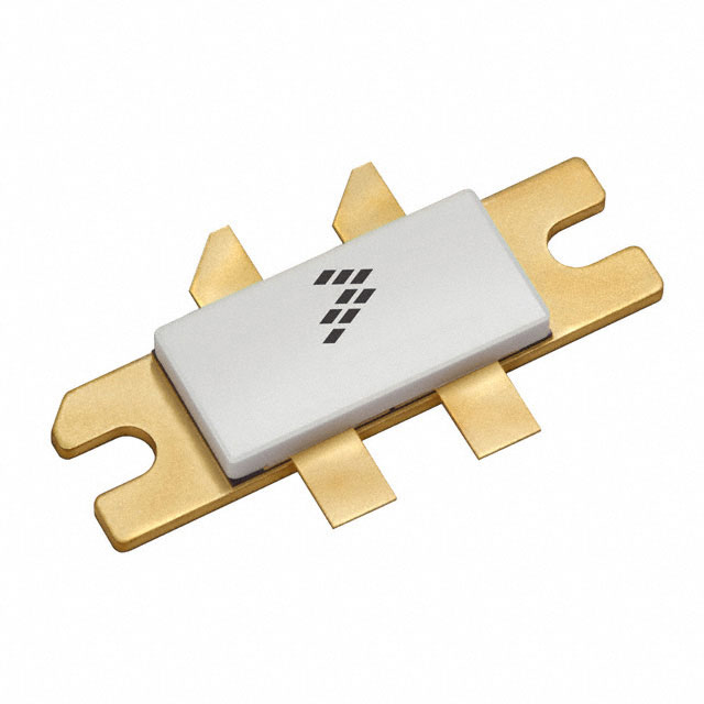
AFV10700H
AFV10700HS
AFV10700GS
960–1215 MHz, 700 W PEAK, 52 V
AIRFAST RF POWER LDMOS
TRANSISTORS
NI--780H--4L
AFV10700H
NI--780S--4L
AFV10700HS
Typical Performance: In 1030 MHz narrowband production test fixture,
IDQ(A+B) = 100 mA
Frequency
(MHz)
1030 (2)
Signal Type
Pulse
(128 sec,
10% Duty Cycle)
VDD
(V)
Pout
(W)
Gps
(dB)
D
(%)
50
730 Peak
19.2
58.5
NI--780GS--4L
AFV10700GS
Narrowband Load Mismatch/Ruggedness
Frequency
(MHz)
1030
(2)
Signal Type
VSWR
Pin
(W)
Test
Voltage
Pulse
(128 sec,
10% Duty Cycle)
> 20:1 at
All Phase
Angles
17.2 Peak
(3 dB
Overdrive)
50
Result
No Device
Degradation
1. Measured in 1030–1090 MHz reference circuit (page 5).
2. Measured in 1030 MHz narrowband production test fixture (page 9).
Features
Internally input and output matched for broadband operation and ease of use
Device can be used in a single--ended, push--pull or quadrature configuration
Qualified up to a maximum of 55 VDD operation
High ruggedness, handles > 20:1 VSWR
Gate A 3
1 Drain A
Gate B 4
2 Drain B
(Top View)
Note: The backside of the package is the
source terminal for the transistor.
Figure 1. Pin Connections
Integrated ESD protection with greater negative gate--source voltage range
for improved Class C operation and gate voltage pulsing
Recommended drivers: MRFE6VS25N (25 W) or MRF6V10010N (10 W)
Included in NXP product longevity program with assured supply for a
minimum of 15 years after launch
2017–2019 NXP B.V.
RF Device Data
NXP Semiconductors
AFV10700H AFV10700HS AFV10700GS
1
�Table 1. Maximum Ratings
Symbol
Value
Unit
Drain--Source Voltage
Rating
VDSS
–0.5, +105
Vdc
Gate--Source Voltage
VGS
–6.0, +10
Vdc
Operating Voltage
VDD
55, +0
Vdc
Storage Temperature Range
Tstg
– 65 to +150
C
TC
–55 to +150
C
Case Operating Temperature Range
Operating Junction Temperature Range
(1,2)
Total Device Dissipation @ TC = 25C
Derate above 25C
TJ
–55 to +225
C
PD
526
2.63
W
W/C
Symbol
Value (2,3)
Unit
ZJC
0.030
C/W
Table 2. Thermal Characteristics
Characteristic
Thermal Impedance, Junction to Case
Pulse: Case Temperature 75C, 730 W Peak, 128 sec Pulse Width,
10% Duty Cycle, 50 Vdc, IDQ(A+B) = 100 mA, 1030 MHz
Table 3. ESD Protection Characteristics
Test Methodology
Class
Human Body Model (per JESD22--A114)
2, passes 2000 V
Charge Device Model (per JESD22--C101)
C3, passes 2000 V
Table 4. Electrical Characteristics (TA = 25C unless otherwise noted)
Characteristic
Off Characteristics
Symbol
Min
Typ
Max
Unit
IGSS
—
—
1
Adc
105
—
—
Vdc
(4)
Gate--Source Leakage Current
(VGS = 5 Vdc, VDS = 0 Vdc)
Drain--Source Breakdown Voltage
(VGS = 0 Vdc, ID = 10 A)
V(BR)DSS
Zero Gate Voltage Drain Leakage Current
(VDS = 50 Vdc, VGS = 0 Vdc)
IDSS
—
—
1
Adc
Zero Gate Voltage Drain Leakage Current
(VDS = 105 Vdc, VGS = 0 Vdc)
IDSS
—
—
10
Adc
Gate Threshold Voltage (4)
(VDS = 10 Vdc, ID = 260 Adc)
VGS(th)
1.3
1.8
2.3
Vdc
Gate Quiescent Voltage
(VDD = 50 Vdc, IDQ(A+B) = 100 mAdc, Measured in Functional Test)
VGS(Q)
1.6
2.1
2.6
Vdc
Drain--Source On--Voltage (4)
(VGS = 10 Vdc, ID = 2.6 Adc)
VDS(on)
—
0.28
—
Vdc
Crss
—
1.16
—
pF
On Characteristics
Dynamic Characteristics (4,5)
Reverse Transfer Capacitance
(VDS = 50 Vdc 30 mV(rms)ac @ 1 MHz, VGS = 0 Vdc)
1.
2.
3.
4.
5.
Continuous use at maximum temperature will affect MTTF.
MTTF calculator available at http://www.nxp.com.
Refer to AN1955, Thermal Measurement Methodology of RF Power Amplifiers. Go to http://www.nxp.com/RF and search for AN1955.
Each side of device measured separately.
Part internally matched both on input and output.
(continued)
AFV10700H AFV10700HS AFV10700GS
2
RF Device Data
NXP Semiconductors
�Table 4. Electrical Characteristics (TA = 25C unless otherwise noted) (continued)
Characteristic
Symbol
Min
Typ
Max
Unit
Functional Tests (In NXP Narrowband Production Test Fixture, 50 ohm system) VDD = 50 Vdc, IDQ(A+B) = 100 mA, Pout = 730 W Peak
(73 W Avg.), f = 1030 MHz, 128 sec Pulse Width, 10% Duty Cycle
Power Gain
Gps
18.0
19.2
21.0
dB
Drain Efficiency
D
54.5
58.5
—
%
Input Return Loss
IRL
—
–15
–9
dB
Load Mismatch/Ruggedness (In NXP Narrowband Production Test Fixture, 50 ohm system) IDQ(A+B) = 100 mA
Frequency
(MHz)
Signal
Type
1030
Pulse
(128 sec,
10% Duty Cycle)
VSWR
> 20:1 at All Phase Angles
Pin
(W)
17.2 Peak
(3 dB Overdrive)
Test Voltage, VDD
Result
50
No Device Degradation
Table 5. Ordering Information
Device
AFV10700HR5
AFV10700HSR5
AFV10700GSR5
Tape and Reel Information
R5 Suffix = 50 Units, 56 mm Tape Width, 13--inch Reel
R5 Suffix = 50 Units, 32 mm Tape Width, 13--inch Reel
Package
NI--780H--4L
NI--780S--4L
NI--780GS--4L
AFV10700H AFV10700HS AFV10700GS
RF Device Data
NXP Semiconductors
3
�TYPICAL CHARACTERISTICS
1.11
Measured with 30 mV (rms) ac @ 1 MHz
VGS = 0 Vdc
10
VDD = 50 Vdc
1.08
NORMALIZED VGS(Q)
C, CAPACITANCE (pF)
100
Crss
1.05
IDQ(A+B) = 100 mA
500 mA
1.02
1000 mA
0.99
0.96
0.93
1
0
10
20
30
40
0.90
–75
50
–50
–25
VDS, DRAIN--SOURCE VOLTAGE (VOLTS)
0
25
50
75
100
TC, CASE TEMPERATURE (C)
Note: Each side of device measured separately.
IDQ (mA)
Figure 2. Capacitance versus Drain--Source Voltage
Slope (mV/C)
100
–2.73
500
–2.39
1500
–2.09
Figure 3. Normalized VGS versus Quiescent
Current and Case Temperature
109
VDD = 50 Vdc
ID = 19.67 Amps
MTTF (HOURS)
108
107
24.39 Amps
106
28.40 Amps
105
104
90
110
130
150
170
190
210
230
250
TJ, JUNCTION TEMPERATURE (C)
Note: MTTF value represents the total cumulative operating time
under indicated test conditions.
MTTF calculator available at http://www.nxp.com.
Figure 4. MTTF versus Junction Temperature – Pulse
AFV10700H AFV10700HS AFV10700GS
4
RF Device Data
NXP Semiconductors
�1030–1090 MHz REFERENCE CIRCUIT – 2.0 3.0 (5.1 cm 7.6 cm)
Table 6. 1030–1090 MHz Performance (In NXP Reference Circuit, 50 ohm system) IDQ(A+B) = 100 mA
Frequency
(MHz)
1030
1090
Signal Type
Pulse
(128 sec, 10% Duty Cycle)
1030
VDD
(V)
Pout
(W)
Gps
(dB)
D
(%)
50
800 Peak
17.5
52.1
700 Peak
19.0
56.1
850 Peak
17.5
51.7
770 Peak
19.2
56.1
52
1090
NOTE: Size of the matching area: 1.3 2.6 (3.3 cm 6.6 cm)
AFV10700H AFV10700HS AFV10700GS
RF Device Data
NXP Semiconductors
5
�1030–1090 MHz REFERENCE CIRCUIT – 2.0 3.0 (5.1 cm 7.6 cm)
C12*
C17
C5
C8*
C18
C13
C6* C7*
C14* C15
C16*
C2*
R1
Q1
C1*
C11*
C3*
C4*
C9* C10*
D85937
*C1, C2, C3, C4, C6, C7, C8, C9, C10, C11, C12, C14 and C16 are mounted vertically.
Figure 5. AFV10700H Reference Circuit Component Layout – 1030–1090 MHz
Table 7. AFV10700H Reference Circuit Component Designations and Values – 1030–1090 MHz
Part
Description
Part Number
Manufacturer
C1
1.5 pF Chip Capacitor
ATC800B1R5BT500XT
ATC
C2, C8, C14
39 pF Chip Capacitor
ATC800B390JT500XT
ATC
C3, C4
4.3 pF Chip Capacitor
ATC800B4R3CT500XT
ATC
C5, C15
2.2 F Chip Capacitor
C3225X7R2A225K230AB
TDK
C6, C12
1000 pF Chip Capacitor
ATC800B102JT50XT
ATC
C7
100 pF Chip Capacitor
ATC800B101JT500XT
ATC
C9
4.7 pF Chip Capacitor
ATC800B4R7CT500XT
ATC
C10, C11
3.3 pF Chip Capacitor
ATC800B3R3CT500XT
ATC
C13
1.0 F Chip Capacitor
GRM31CR72A105KA01L
Murata
C16
270 pF Chip Capacitor
ATC800B271JT200XT
ATC
C17, C18
470 F, 63 V Electrolytic Capacitor
MCGPR63V477M13X26--RH
Multicomp
Q1
RF High Power LDMOS Transistor
AFV10700H
NXP
R1
22 , 1/8 W Chip Resistor
RK73H2ATTD22R0F
KAO Speer
PCB
Rogers RO3010 0.025, r = 11.2
D85937
MTL
AFV10700H AFV10700HS AFV10700GS
6
RF Device Data
NXP Semiconductors
�TYPICAL CHARACTERISTICS – 1030–1090 MHz
REFERENCE CIRCUIT
21
70
Gps
60
D
19
50
1030 MHz
1030 MHz
18
40
17
30
16
20
VDD = 50 Vdc, IDQ(A+B) = 100 mA
Pulse Width = 128 sec, Duty Cycle = 10%
15
0
100
200
300
400
500
600
700
800
D DRAIN EFFICIENCY (%)
Gps, POWER GAIN (dB)
1090 MHz
1090 MHz
20
10
900 1000
Pout, OUTPUT POWER (WATTS) PEAK
Figure 6. Power Gain and Drain Efficiency versus
Output Power – 50 V
70
21
Gps, POWER GAIN (dB)
1090 MHz
Gps
60
D
1030 MHz
19
50
1030 MHz
18
40
30
17
16
20
VDD = 52 Vdc, IDQ(A+B) = 100 mA
Pulse Width = 128 sec, Duty Cycle = 10%
15
0
200
400
600
800
1000
D DRAIN EFFICIENCY (%)
1090 MHz
20
10
1200
Pout, OUTPUT POWER (WATTS) PEAK
Figure 7. Power Gain and Drain Efficiency versus
Output Power – 52 V
AFV10700H AFV10700HS AFV10700GS
RF Device Data
NXP Semiconductors
7
�1030–1090 MHz REFERENCE CIRCUIT
Zo = 5
f = 1090 MHz
Zload
f = 1030 MHz
f = 1030 MHz
Zsource
f = 1090 MHz
f
MHz
Zsource
Zload
1030
2.3 – j1.7
0.91 – j0.76
1090
2.0 – j1.9
0.88 – j0.47
Zsource = Test circuit impedance as measured from
gate to ground.
Zload
50
= Test circuit impedance as measured
from drain to ground.
Output
Matching
Network
Device
Under
Test
Input
Matching
Network
Zsource
50
Zload
Figure 8. Series Equivalent Source and Load Impedance – 1030–1090 MHz
AFV10700H AFV10700HS AFV10700GS
8
RF Device Data
NXP Semiconductors
�1030 MHz NARROWBAND PRODUCTION TEST FIXTURE – 4.0 5.0 (10.2 cm 12.7 cm)
C1
C3
C25
B1
AFV10700H
Rev. 0
C5
C7
D89532
C17
C12
R1
Coax1
C27
Coax3
L1
C14*
C9
C11
C16
C22*
C23*
C24*
CUT OUT AREA
C10
Coax2
C19*
C20*
C21*
C15*
L2
R2
Coax4
C13
C2
B2
C4
C8
C6
C18
C26
C28
*C14, C15, C19, C20, C21, C22, C23 and C24 are mounted vertically.
Figure 9. AFV10700H Narrowband Test Circuit Component Layout – 1030 MHz
Table 8. AFV10700H Narrowband Test Circuit Component Designations and Values – 1030 MHz
Part
Description
Part Number
Manufacturer
B1, B2
Short RF Bead
2743019447
Fair--Rite
C1, C2
22 F, 35 V Tantalum Capacitor
T491X226K035AT
Kemet
C3, C4
2.2 F Chip Capacitor
C1825C225J5RAC
Kemet
C5, C6
0.1 F Chip Capacitor
CDR33BX104AKWS
AVX
C7, C8, C19, C20, C21, C22, C23, C24
43 pF Chip Capacitor
ATC100B430JT500XT
ATC
C9, C10
3.3 pF Chip Capacitor
ATC100B3R3CT500XT
ATC
C11
0.7 pF Chip Capacitor
ATC100B0R7BT500XT
ATC
C12, C13
36 pF Chip Capacitor
ATC100B360JT500XT
ATC
C14, C15
5.1 pF Chip Capacitor
ATC100B5R1CT500XT
ATC
C16
5.6 pF Chip Capacitor
ATC100B5R6CT500XT
ATC
C17, C18
0.01 F Chip Capacitor
C1825C103K1GACTU
Kemet
C25, C26, C27, C28
470 F, 63 V Electrolytic Capacitor
MCGPR63V477M13X26--RH
Multicomp
Coax1, Coax2, Coax3, Coax4
35 Semi Rigid Coax 1.98 Shield Length
HSF--141--35--C
Hongsen Cable
L1, L2
12 nH Inductor, 3 Turns
GA3094--ALC
Coilcraft
R1, R2
5.6 1/4 W Chip Resistor
CRCW12065R60FKEA
Vishay
PCB
Arlon, AD255A, 0.03, r = 2.55
D89532
MTL
AFV10700H AFV10700HS AFV10700GS
RF Device Data
NXP Semiconductors
9
�TYPICAL CHARACTERISTICS – 1030 MHz, TC = 25_C
PRODUCTION TEST FIXTURE
70
19.5
60
Gps
50
D
18.5
40
18.0
30
17.5
20
17.0
50
24
Gps, POWER GAIN (dB)
22
100
300
200
20
500 mA
19
100 mA
17
50
500
100
1000
Pout, OUTPUT POWER (WATTS) PEAK
Pout, OUTPUT POWER (WATTS) PEAK
Figure 10. Power Gain and Drain Efficiency
versus Output Power
Figure 11. Power Gain versus Output Power and
Quiescent Drain Current
1200
IDQ(A+B) = 100 mA, f = 1030 MHz
Pulse Width = 128 sec, Duty Cycle = 10%
20
18
50 V
16
45 V
14
35 V
12
10
50
IDQ(A+B) = 1000 mA
18
10
1000
700
500
21
Gps, POWER GAIN (dB)
20.0
19.0
VDD = 50 Vdc, f = 1030 MHz
Pulse Width = 128 sec, Duty Cycle = 10%
80
40 V
VDD = 30 V
100
500
200
Pout, OUTPUT POWER (WATTS) PEAK
Gps, POWER GAIN (dB)
20.5
22
90
VDD = 50 Vdc, IDQ(A+B) = 100 mA, f = 1030 MHz
Pulse Width = 128 sec, Duty Cycle = 10%
D, DRAIN EFFICIENCY (%)
21.0
VDD = 50 Vdc, IDQ(A+B) = 100 mA, f = 1030 MHz
Pulse Width = 128 sec, Duty Cycle = 10%
1000
TC = –55_C
85_C
600
400
200
0
28
1000
25_C
800
32
30
34
36
38
40
42
44
Pin, INPUT POWER (dBm) PEAK
Pout, OUTPUT POWER (WATTS) PEAK
Figure 12. Power Gain versus Output Power
and Drain Voltage
f
(MHz)
P1dB
(W)
P3dB
(W)
1030
740
883
Figure 13. Output Power versus Input Power
24
Gps, POWER GAIN (dB)
80
VDD = 50 Vdc, IDQ(A+B) = 100 mA, f = 1030 MHz
Pulse Width = 128 sec, Duty Cycle = 10%
22
70
TC = 25_C
D
85_C
20
50
TC = –55_C
18
Gps
16
25_C
0
200
400
600
800
40
30
85_C
14
12
60
–55_C
D, DRAIN EFFICIENCY (%)
26
20
1000
10
1200
Pout, OUTPUT POWER (WATTS) PEAK
Figure 14. Power Gain and Drain Efficiency versus
Output Power
AFV10700H AFV10700HS AFV10700GS
10
RF Device Data
NXP Semiconductors
�1030 MHz NARROWBAND PRODUCTION TEST FIXTURE
f
MHz
Zsource
Zload
1030
4.0 – j6.9
3.9 – j1.4
Zsource = Test circuit impedance as measured from
gate to gate, balanced configuration.
Zload
50
Input
Matching
Network
= Test circuit impedance as measured
from drain to drain, balanced configuration.
+
Device
Under
Test
--
--
+
Zsource
Zload
Output
Matching
Network
50
Figure 15. Series Equivalent Source and Load Impedance – 1030 MHz
AFV10700H AFV10700HS AFV10700GS
RF Device Data
NXP Semiconductors
11
�PACKAGE DIMENSIONS
AFV10700H AFV10700HS AFV10700GS
12
RF Device Data
NXP Semiconductors
�AFV10700H AFV10700HS AFV10700GS
RF Device Data
NXP Semiconductors
13
�AFV10700H AFV10700HS AFV10700GS
14
RF Device Data
NXP Semiconductors
�AFV10700H AFV10700HS AFV10700GS
RF Device Data
NXP Semiconductors
15
�AFV10700H AFV10700HS AFV10700GS
16
RF Device Data
NXP Semiconductors
�AFV10700H AFV10700HS AFV10700GS
RF Device Data
NXP Semiconductors
17
�PRODUCT DOCUMENTATION, SOFTWARE AND TOOLS
Refer to the following resources to aid your design process.
Application Notes
AN1908: Solder Reflow Attach Method for High Power RF Devices in Air Cavity Packages
AN1955: Thermal Measurement Methodology of RF Power Amplifiers
Engineering Bulletins
EB212: Using Data Sheet Impedances for RF LDMOS Devices
Software
Electromigration MTTF Calculator
RF High Power Model
.s2p File
Development Tools
Printed Circuit Boards
REVISION HISTORY
The following table summarizes revisions to this document.
Revision
Date
Description
0
May 2017
Initial release of data sheet
1
Jan. 2018
Added part number AFV10700GS, p. 1
Production test fixture, Typical Characteristic graphs: clarified temperature condition, p. 10
Added NI--780GS--4L package isometric, p. 1, and Mechanical Outline, pp. 16–17
2
Aug. 2019
Overview copy and device description: updated to reflect frequency band operation from 960–1215 MHz,
p. 1
Typical Performance table: added 960–1215 MHz performance data, p. 1
Table 6, 1030–1090 Component Layout Parts List: updated the part number and description for C16 and
R1, p. 6
AFV10700H AFV10700HS AFV10700GS
18
RF Device Data
NXP Semiconductors
�How to Reach Us:
Home Page:
nxp.com
Web Support:
nxp.com/support
Information in this document is provided solely to enable system and software
implementers to use NXP products. There are no express or implied copyright licenses
granted hereunder to design or fabricate any integrated circuits based on the information
in this document. NXP reserves the right to make changes without further notice to any
products herein.
NXP makes no warranty, representation, or guarantee regarding the suitability of its
products for any particular purpose, nor does NXP assume any liability arising out of the
application or use of any product or circuit, and specifically disclaims any and all liability,
including without limitation consequential or incidental damages. “Typical” parameters
that may be provided in NXP data sheets and/or specifications can and do vary in
different applications, and actual performance may vary over time. All operating
parameters, including “typicals,” must be validated for each customer application by
customer’s technical experts. NXP does not convey any license under its patent rights
nor the rights of others. NXP sells products pursuant to standard terms and conditions of
sale, which can be found at the following address: nxp.com/SalesTermsandConditions.
NXP, the NXP logo and Airfast are trademarks of NXP B.V. All other product or service
names are the property of their respective owners.
E 2017–2019 NXP B.V.
AFV10700H AFV10700HS AFV10700GS
Document
Number:
RF
Device
Data AFV10700H
Rev. 2,Semiconductors
08/2019
NXP
19
�