Freescale Semiconductor
Technical Data
Document Number: MC06XS3517
Rev. 5.0, 4/2014
Smart High-side Switch Module
(Triple 6.0 mOhm and Dual
17 mOhm)
06XS3517
The 06XS3517 device is a five channel 12 V high-side switch module with
integrated control and a high number of protective and diagnostic
functions. It is designed for automotive lighting and industrial applications.
The low RDS(on) channels (three 6.0 mOhm, two 17 mOhm) can control
different types of lighting applications; bulbs, Xenon-HID lights, and LEDs.
Control, device configuration, and diagnostics are performed through a
16-bit SPI interface (3.3 V or 5.0 V). When communication with the
external microcontroller or VDD is lost, the device enters a fail-safe
operation mode, but remains operational, controllable, and protected.
The channels are controlled by an external clock signal and allow
staggered switch-on delay, to improve EMC performances. Programmable
output voltage slew rates (individually programmable) further help improve
EMC performance. To avoid shutting off the device upon inrush current
while still being able to closely track the load current, a dynamic
overcurrent threshold profile is featured. Load current in each channel can
be sensed. The duty cycle of the channels can be controlled independently
and the switching frequency of each of them can be doubled. The
06XS3517 is housed in a non-leaded Power QFN package with an
exposed pad. This device is powered using SMARTMOS technology.
Features
•
•
•
•
•
•
•
•
•
•
Three 6.0 mOhm and two 17 mOhm protected high-side switches
Optional sixth channel with an external smart MOSFET
16-bit SPI communication interface with daisy chain capability
Accurate temperature and current sensing
Fail-safe mode including autorestart
PWM module with programmable switch-on delay and frequency
prescaler
Overvoltage, undervoltage, overcurrent, overtemperature, and reverse
battery protections
Dedicated bulb overcurrent protection with inrush current handling
Sleep mode with low current consumption
Normal operating range 7.0 V to 20 V, extended operating range 6.0 V
- 28 V
12 V
5.0 V
FK SUFFIX
98ART10511D
24-PIN PQFN
Applications
• Low-voltage automotive lighting
• Halogen bulbs
• Light-emitting diodes (LEDs)
• High beam
• Low beam
• Flashers
• Low-voltage industrial lighting
12 V
VBAT
LIMP
CP
FLASHER
IGN
OUT1
RSTB
OUT2
CLOCK
MCU
Bottom View
06XS3517
VCC
Watchdog
High-side Switch
OUT3
CSB
FOG
OUT4
SO
OUT5
SI
FETIN
SCLK
CSNS
GND
FETOUT
Smart
Switch
Figure 1. 06XS3517 Simplified Application Diagram
© Freescale Semiconductor, Inc., 2012 - 2014. All rights reserved.
�ORDERABLE PARTS
ORDERABLE PARTS
Table 1. Orderable Part Variations
Part Number
Temperature (TA)
Package
MC06XS3517AFK(1)
-40°C to 125 °C
24 PQFN
Notes
1. To order parts in Tape & Reel, add the R2 suffix to the part number.
MC06XS3517
2
Analog Integrated Circuit Device Data
Freescale Semiconductor
�INTERNAL BLOCK DIAGRAM
INTERNAL BLOCK DIAGRAM
VCC
VBAT
Vcc failure
detection
RUP
Internal
Regulator
CP
OV/UV/POR
detections
Charge
Pump
CSB
SO
SI
SCLK
Gate Drive
drain/gate clamp
Logic
LED Control
RDWN
OUT1
(* Park)
Overcurrent
Detection
CLOCK
LIMP
FOG
Open Load
Detection
FLASHER
IGN
RSTB
Overtemperature
Detection
OUT1
RDWN
Overtemperature
Prewarning
OUT2
OUT2
(* LBeam)
OUT3
OUT3
(* HBeam)
OUT4
OUT4
(* Fog)
OUT5
OUT5
(* Flash)
Shared Output Current
sensing pin (Analog MUX)
CSNS
Temperature
Feedback
FETIN
(* Sense In)
Current Recopy
Synchronization
VCC
Driver for an External
SMART MOSFET
GND
FETOUT
(* Logic Level)
* See 06XS3517 Typical Application
Figure 2. 06XS3517 Simplified Internal Block Diagram
MC06XS3517
Analog Integrated Circuit Device Data
Freescale Semiconductor
3
�PIN CONNECTIONS
CSB
FOG
LIMP
CLOCK
FLASHER
RSTB
IGN
FETIN
9
8
7
6
5
4
3
2
1
CP
16
GND
17
OUT5
18
VCC
SCLK
Transparent
Top View
SO
13 12 11 10
FETOUT
SI
PIN CONNECTIONS
14
GND
24
CSNS
23
GND
22
OUT1
15
VBAT
19
20
21
OUT4
OUT3
OUT2
Figure 3. 06XS3517 Pin Connections
Table 2. 06XS3517 Pin Definitions
A functional description of each pin can be found in the Functional Pin Description section beginning on page 20.
Pin
Number
Pin Name
Pin Function
Formal Name
1
FETIN
Input
External FET Input
2
IGN
Input
Ignition Input
(Active High)
This input wakes the device. It also controls the Outputs 1 and 2 in case of Fail
mode activation. This pin has an internal pull-down resistor.
3
RSTB
Input
Reset
This input wakes the device. It is also used to initialize the device configuration
and fault registers through the SPI. This digital pin has a passive internal pulldown.
4
FLASHER
Input
Flasher Input
(Active High)
This input wakes the device and allows control over channel 5. (FLASHER) This
pin has an internal pull-down resistor.
5
CLOCK
Input/Output
Clock Input
Definition
This pin receives the current sense signal of the external smart MOSFET.
This pin state depends on RSTB logic level.
As long as RSTB input pin is set to logic [0], this pin is pulled up to report wake
events. Otherwise, the PWM frequency and timing are generated from this
digital clock input by the PWM module.
This pin has a passive internal pull-down.
6
LIMP
Input
Limp Home Input
(Active High)
The Fail mode can be activated by this digital input. This pin has a passive
internal pull-down.
7
FOG
Input
FOG Input (Active
high)
This input wakes the device. This pin has a passive internal pull-down.
8
CSB
Input
Chip Select
(Active Low)
When this digital signal is high, SPI signals are ignored. Asserting this pin low
starts a SPI transaction. The transaction is signaled as completed when this
signal returns high. This pin has a passive internal pull-up resistance.
MC06XS3517
4
Analog Integrated Circuit Device Data
Freescale Semiconductor
�PIN CONNECTIONS
Table 2. 06XS3517 Pin Definitions (continued)
A functional description of each pin can be found in the Functional Pin Description section beginning on page 20.
Pin
Number
Pin Name
Pin Function
Formal Name
Definition
9
SCLK
Input
SPI Clock Input
This digital input pin is connected to the master microcontroller providing the
required bit shift clock for SPI communication. This pin has a passive internal
pull-down resistance.
10
SI
Input
Master-Out SlaveIn
11
VCC
Power
Logic Supply
12
SO
Output
Master-In SlaveOut
SPI data is sent to the MCU by this pin. This data output changes on the
negative edge of SCLK and when CSB is high, this pin is high-impedance.
13
FETOUT
Output
External FET Gate
This pin outputs a logic level that can be used to control an external smart
MOSFET. This output is also called OUT6.
This data input is sampled on the positive edge of the SCLK. This pin has a
passive internal pull-down resistance.
SPI logic power supply.
If OUT6 is not used in the application, this output pin is set to logic high when
the current sense output becomes valid when CSNS sync SPI bit is set to logic
[1].
This pin is the ground for the logic and analog circuitry of the device.
14,17,23
GND
Ground
Ground
15
VBAT
Power
Battery Input
Power supply pin.
16
CP
Output
Charge Pump
This pin is the connection for an external tank capacitor (for internal use only).
22
18
OUT1
OUT5
Output
Output 1
Output 5
Protected 17 mOhm high-side switch output terminals.
21
20
19
OUT2
OUT3
OUT4
Output
Output 2
Output 3
Output 4
Protected 6.0 mOhm high-side switch output terminals.
24
CSNS
Output
Current Sense
Output
This pin is outputs the current sense signal of OUT1:OUT5, FET IN current, and
it is used externally to generate a ground-referenced voltage for the
microcontroller to monitor output current. If desired, this pin can also report a
voltage proportional to the temperature on the GND flag.
OUT1:OUT5, FET in current sensing and temperature sensing are activated
through the SPI interface.
Notes
1. The pins 14, 17, and 23 must be shorted on the board.
MC06XS3517
Analog Integrated Circuit Device Data
Freescale Semiconductor
5
�ELECTRICAL CHARACTERISTICS
MAXIMUM RATINGS
ELECTRICAL CHARACTERISTICS
MAXIMUM RATINGS
Table 3. Maximum Ratings
All voltages are with respect to ground, unless mentioned otherwise. Exceeding these ratings may cause malfunction or
permanent device damage.
Parameter
Symbol
Value
Unit
ELECTRICAL RATINGS
Overvoltage Test Range (all OUT[1:5] ON with nominal DC current)
VBAT
V
Maximum operating voltage
28
Load dump (400 ms) @ 25 °C
40
Reverse Polarity Voltage Range (all OUT[1:5] ON with nominal DC current)
VBAT
2.0 Min @ 25°C
V
- 18
VCC Supply Voltage
VCC
OUT[1:5] Voltage
VOUT
-0.3 to 5.5
V
Positive
40
Negative (ground disconnected)
-16
Digital Current in Clamping Mode (SI, SCLK, CSB, RSTB, IGN, FLASHER, LIMP,
and FOG)
FETIN Input Current
IIN
IFETIN
V
±1.0
mA
+10
mA
-1.0
SO, FETOUT, CLOCK, and CSNS Outputs Voltage
VSO
- 0.3 to VCC + 0.3
E1,5
30
E2,3,4
100
Outputs Clamp Energy Using Single Pulse Method (L = 2.0 mH; R = 0.0 Ohm;
VBAT = 14 V @150 °C initial)
OUT[1,5]
OUT[2:4]
ESD
Voltage(2)
V
mJ
VESD
V
Human Body Model (HBM)
±2000
Human Body Model (HBM) OUT [1:5], VPWR, and GND
±8000
Charge Device Model (CDM)
Corner Pins (1, 13, 19, 21)
All Other Pins (2-12, 14-18, 20, 22-24)
±750
±500
Notes
2. ESD testing is performed in accordance with the Human Body Model (HBM) (CZAP = 100 pF, RZAP = 1500 Ω) and the Charge Device
Model.
MC06XS3517
6
Analog Integrated Circuit Device Data
Freescale Semiconductor
�ELECTRICAL CHARACTERISTICS
MAXIMUM RATINGS
Table 3. Maximum Ratings (continued)
All voltages are with respect to ground, unless mentioned otherwise. Exceeding these ratings may cause malfunction or
permanent device damage.
Parameter
Symbol
Value
Unit
Ambient
TA
- 40 to 125
Junction
TJ
- 40 to 150
Peak Package Reflow Temperature During Reflow(3)
TPPRT
260
°C
Storage Temperature
TSTG
- 55 to 150
°C
RθJC
1.0
°K/W
THERMAL RATINGS
Operating Temperature
°C
THERMAL RESISTANCE
Thermal Resistance, Junction to Case(4)
Notes
3. Pin soldering temperature limit is for 40 seconds maximum duration. Not designed for immersion soldering. Exceeding these limits may
cause malfunction or permanent damage to the device.
4. Typical value guaranteed per design.
MC06XS3517
Analog Integrated Circuit Device Data
Freescale Semiconductor
7
�ELECTRICAL CHARACTERISTICS
STATIC ELECTRICAL CHARACTERISTICS
STATIC ELECTRICAL CHARACTERISTICS
Table 4. Static Electrical Characteristics
Characteristics noted under conditions 3.0 V ≤ VCC ≤ 5.5 V, 7.0 V ≤ VBAT ≤ 20 V, - 40 °C ≤ TA ≤ 125 °C, GND = 0 V, unless
otherwise noted. Typical values noted reflect the approximate parameter means at TA = 25 °C under nominal conditions, unless
otherwise noted.
Characteristic
Symbol
Min
Typ
Max
Full performance and short-circuit
7.0
–
20.0
Extended voltage range(5)
6.0
–
28.0
Unit
POWER INPUTS (VBAT, VCC)
Battery Supply Voltage Range
VBAT
V
Battery Supply Undervoltage (UV flag is set ON)
VBATUV
5.0
5.5
6.0
V
Battery Supply Overvoltage (OV flag is set ON)
VBATOV
27.5
30
32.5
V
(6)
VBATCLAMP
40
–
48
V
Battery Voltage Clamp
Battery Supply Power on Reset
V
If VBAT < 5.5 V, VBAT = VCC
VBATPOR1
2.0
–
3.0
If VBAT < 5.5 V, VCC = 0
VBATPOR2
2.0
–
4.0
Sleep state current, outputs opened
IBATSLEEP1
–
0.5
5.0
μA
Sleep state current, outputs grounded
IBATSLEEP2
–
0.5
5.0
μA
IBAT
–
10.0
20.0
mA
VCC
3.0
–
5.5
V
VCCUV
2.2
2.5
2.8
V
–
0.2
5.0
No SPI
–
–
2.6
3.0 MHz SPI communication
–
–
5.0
VBAT Supply Current @ 25 °C and VBAT = 12 V and VCC = 5.0 V
Normal mode, IGN = 5.0 V, RSTB = 5.0 V, outputs open
Digital Supply Voltage Range, Full Performance
Digital Supply Undervoltage (VCC Failure)
Sleep Current Consumption on VCC @ 25 °C and VBAT = 12 V
μA
ICCSLEEP
Output OFF
Supply Current Consumption on VCC and VBAT = 12 V
ICC
mA
LOGIC INPUT/OUTPUT (IGN, CS, CSNS, SI, SCLK, CLOCK, SO, FLASHER, RST, LIMP, FOG)
Input High Logic Level(7)
VIH
2.0
–
–
V
Input Low Logic Level(7)
VIL
–
–
0.8
V
VIGNTH
1.0
–
2.2
V
7.5
–
13
- 2.0
–
-0.3
RUP
100
250
500
kOhm
RDWN
100
250
500
kOhm
Voltage Threshold for Wake-up (IGN, FLASHER, FOG, RST)
Input Clamp Voltage (IGN, FLASHER, LIMP, FOG, CS, SCLK, SI, RST)
VCL_POS
I = 1.0 mA
Input Forward Voltage (IGN, FLASHER, LIMP, FOG, CS, SCLK, SI, RST)
VCL_NEG
I = -1.0 mA
Input Passive Pull-up Resistance on CS Input(8)
Input Passive Pull-down Resistance on SI, SCLK, FLASHER, IGN, FOG,
CLOCK, LIMP, RST pins(8)
V
V
Notes
5. In extended mode, the functionality is guaranteed but not the electrical parameters.
6. Outputs shorted to ground, IOUT = + 500 mA and IOUT = OCHI (guaranteed by design).
7.
8.
Valid for RST, SI, SCLK, CS, CLOCK, IGN, FLASHER, FOG, and LIMP pins.
Valid for the following input voltage range: -0.3 V to VCC +0.3 V.
MC06XS3517
8
Analog Integrated Circuit Device Data
Freescale Semiconductor
�ELECTRICAL CHARACTERISTICS
STATIC ELECTRICAL CHARACTERISTICS
Table 4. Static Electrical Characteristics (continued)
Characteristics noted under conditions 3.0 V ≤ VCC ≤ 5.5 V, 7.0 V ≤ VBAT ≤ 20 V, - 40 °C ≤ TA ≤ 125 °C, GND = 0 V, unless
otherwise noted. Typical values noted reflect the approximate parameter means at TA = 25 °C under nominal conditions, unless
otherwise noted.
Characteristic
Symbol
Min
Typ
Max
Unit
LOGIC INPUT/OUTPUT (IGN, CS, CSNS, SI, SCLK, CLOCK, SO, FLASHER, RST, LIMP, FOG) (CONTINUED)
SO High-state Output Voltage
VSOH
IOH = 1.0 mA
SO Low-state Output Voltage
VCC
0.8
0.95
–
VSOL
IOL = -1.6 mA
V
–
0.2
0.4
CLOCK Output Voltage Reporting Wake-up Event (ICLOCK=1.0mA)
VCLOCKH
0.8
0.95
–
VCC
SO and CSNS Tri-state Leakage Current
ISOLEAK
- 1.0
0.0
1.0
μA
Current Sense Output Clamp Voltage
VCSNS
5.0
6.0
7.0
- 22.0
–
-16.0
Sleep mode, outputs grounded, TA = 25 °C
–
0.0
2.0
Sleep mode, outputs grounded, TA = 125 °C
–
0.0
3.0
Normal mode, outputs grounded
–
20
25
CSNS open and IOUT[1:5] = IFSR
V
OUTPUTS (OUT 1-5)
Output Negative Clamp Voltage
VOUT
IOUT = - 500 mA, Outputs OFF
Output Leakage Current in OFF State
Current Sense Error(9) over the Full Voltage and Temperature Range
V
ILEAK(off)
µA
ΔICS / ICS
%
%Full Scale Range (FSR), LED Control bit = 0, Channels 1,5 (17 mOhm)
point @ 0.75 FSR
-14
0.0
14
point @ 0.50 FSR
-15
0.0
15
point @ 0.25 FSR
-17
0.0
17
point @ 0.1 FS
-25
0.0
25
point @ 0.05FSR
-40
0.0
40
-14
0.0
14
-15
0.0
15
-17
0.0
17
-34
0.0
34
Current Sense error with one calibration point (50% FSR, VBAT = 13.5 at
25 °C(10)
-6.0
–
6.0
%
Current Sense error with one calibration point (50% FSRLED, VBAT = 13.5 at
25 °C(10)
-6.0
–
6.0
%
–
±280
± 400
155
175
195
% Full-Scale Range (FSR), LED Control bit =0, Channels 2,3,4
(6.0 mOhm)
point @ 0.75 FSR
point @ 0.50 FSR
point @ 0.25 FSR
point @ 0.1 FSR
Temperature Drift of Current Sense Output(11)
Δ ICS /ΔT
VBAT = 13.5 V, IOUT1,5 = 2.8 A, IOUT2-4 = 5.5 A, reference taken at
TA=25 °C
Overtemperature Shutdown
TOTS
ppm/°C
°C
MC06XS3517
Analog Integrated Circuit Device Data
Freescale Semiconductor
9
�ELECTRICAL CHARACTERISTICS
STATIC ELECTRICAL CHARACTERISTICS
Table 4. Static Electrical Characteristics (continued)
Characteristics noted under conditions 3.0 V ≤ VCC ≤ 5.5 V, 7.0 V ≤ VBAT ≤ 20 V, - 40 °C ≤ TA ≤ 125 °C, GND = 0 V, unless
otherwise noted. Typical values noted reflect the approximate parameter means at TA = 25 °C under nominal conditions, unless
otherwise noted.
Characteristic
Symbol
Min
Typ
Max
Unit
Notes
9. 10 V < VBAT < 16 V. ΔICS / ICS = (measured ICS - targeted ICS)/ targeted ICS with targeted ICS = 5.0 mA. Test conditions of accuracy
measurement of point I(HS[1]) @ 0.05*FSR: I(HS[5]) = 0, I(HS[2]) = I(HS[3]) = I(HS[4]) =8.0 A
10. Based on statistical analysis covering 99.74% of parts, except 10% of FSR. Refer to Current Sense section for more details.
11. Based on statistical data. Not production tested. Δ ICS /ΔT=[(measured ICS at T1 - measured ICS at T2) / measured ICS at room] / (T1 -T2)
OUTPUTS (OUT 1-5) (CONTINUED)
Thermal Prewarning(12)
TOTSWARN
110
125
140
°C
VOUT_TH
0.475
0.5
0.525
VBAT
VBAT = 13.5 V
–
–
17
VBAT = 7.0 V
–
–
26.7
–
–
28.9
–
–
34
Output Voltage Threshold
CHANNEL 1 - PARKING LIGHT (17 mOhm CHANNEL)
Output Drain-to-Source ON Resistance (IOUT = 2.8 A, TA = 25 °C)
Output Drain-to-Source ON Resistance (IOUT = 2.8 A, VBAT = 13.5 V,
TA = 150 °C)(12)
Reverse Output ON Resistance (IOUT = -2.8 A, TA = 25 °C)(13)
RDS(on)25
mOhm
RDS(on)150
mOhm
RSD(on)
VBAT = -12 V
mOhm
High Overcurrent Shutdown Threshold 1, VBAT = 16 V
IOCHI1
48
56.2
72
A
High Overcurrent Shutdown Threshold 2
IOCHI2
21.0
25.8
30.5
A
Low Overcurrent Shutdown Threshold
IOCLO
9.0
11.5
14
A
IOL
0.08
0.3
0.77
A
4.0
10.0
20.0
ICS FSR
–
9.5
–
A
RSC1(OUT1)
225
–
–
mOhm
Open Load-current Threshold in ON State(14)
Open Load-current Threshold in ON State with LED(15)
IOLLED
VOUT = VBAT - 0.8 V
Current Sense Full-scale Range(16)
Severe Short-circuit Impedance Range
(17)
mA
CHANNEL 2 - LOW BEAM (6.0 mOhm CHANNEL)
Output Drain-to-Source ON Resistance (IOUT = 5.5 A, TA = 25 °C)
RDS(on)25
mOhm
VBAT = 13.5 V
–
–
6.0
VBAT = 7.0 V
–
–
9.0
–
–
10.2
–
–
12.0
Output Drain-to-Source ON Resistance (IOUT = 5.5 A, VBAT = 13.5 V,
RDS(on)150
TA = 150 °C)(17)
Reverse Source-to-Drain ON Resistance (IOUT = -5.5 A, TA = 25 °C)(18)
mOhm
RSD(on)
VBAT = -12 V
mOhm
High Overcurrent Shutdown Threshold 1, VBAT = 16 V
IOCHI1
96
123
150
A
High Overcurrent Shutdown Threshold 2
IOCHI2
40
50.5
61
A
MC06XS3517
10
Analog Integrated Circuit Device Data
Freescale Semiconductor
�ELECTRICAL CHARACTERISTICS
STATIC ELECTRICAL CHARACTERISTICS
Table 4. Static Electrical Characteristics (continued)
Characteristics noted under conditions 3.0 V ≤ VCC ≤ 5.5 V, 7.0 V ≤ VBAT ≤ 20 V, - 40 °C ≤ TA ≤ 125 °C, GND = 0 V, unless
otherwise noted. Typical values noted reflect the approximate parameter means at TA = 25 °C under nominal conditions, unless
otherwise noted.
Characteristic
Symbol
Min
Typ
Max
Unit
Notes
12. Parameter guaranteed by design, however, it is not production tested.
13. Source-to-Drain ON Resistance (Reverse Drain-to-Source ON Resistance) with negative polarity VBAT.
14.
15.
16.
OLLED1, bit D0 in SI data is set to [0].
OLLED1, bit D0 in SI data is set to [1].
For typical value of ICS FSR, ICSNS = 5.0 mA.
17.
18.
Parameter guaranteed by design; however, it is not production tested.
Source-to-Drain ON resistance (Reverse Drain-to-Source ON Resistance) with negative polarity VBAT.
MC06XS3517
Analog Integrated Circuit Device Data
Freescale Semiconductor
11
�ELECTRICAL CHARACTERISTICS
STATIC ELECTRICAL CHARACTERISTICS
Table 4. Static Electrical Characteristics (continued)
Characteristics noted under conditions 3.0 V ≤ VCC ≤ 5.5 V, 7.0 V ≤ VBAT ≤ 20 V, - 40 °C ≤ TA ≤ 125 °C, GND = 0 V, unless
otherwise noted. Typical values noted reflect the approximate parameter means at TA = 25 °C under nominal conditions, unless
otherwise noted.
Characteristic
Symbol
Min
Typ
Max
28
35
42
17
22.5
28
0.15
0.62
1.55
Unit
CHANNEL 2 - LOW BEAM (6.0 mOhm CHANNEL) (CONTINUED)
Low Overcurrent Shutdown Threshold
IOCLO
Optional Xenon lamp
Optional H7 bulb
Open Load Current Threshold in ON State
(19)
Open Load Current Threshold in ON State with
IOL
LED(20)
A
IOLLED
VOL = VBAT - 0.8 V
mA
4.0
10.0
20.0
–
30
–
–
19
–
65
–
–
VBAT = 13.5 V
–
–
6.0
VBAT = 7.0 V
–
–
9.0
Current Sense Full-scale Range
(21)
ICS FSR
Optional Xenon bulb
Optional H7 bulb
Severe Short-circuit Impedance Range
RSC1(OUT2)
(22)
A
A
mOhm
CHANNEL 3- HIGH BEAM (6.0 mOhm CHANNEL)
Output Drain-to-Source ON Resistance (IOUT = 5.5 A, TA = 25 °C)
Output Drain-to-Source ON Resistance (IOUT = 5.5 A, VBAT = 13.5 V,
RDS(on)25
RDS(on)150
(22)
TA = 150 °C)
Reverse Source-to-Drain ON Resistance (IOUT = -5.5 A, TA = 25
°C)(23)
mOhm
mOhm
–
–
10.2
–
–
12
RSD(on)25
VBAT = -12 V
mOhm
High Overcurrent Shutdown Threshold 1, VBAT = 16 V
IOCHI1
96
123
150
A
High Overcurrent Shutdown Threshold 2
IOCHI2
40
50.5
61
A
Low Overcurrent Shutdown Threshold
IOCLO
17
22.5
28
0.15
0.62
1.55
4.0
10.0
20.0
ICS FSR
–
19
–
A
RSC1(OUT3)
65
–
–
mOhm
H7 Bulb
Open Load Current Threshold in ON State(24)
Open Load Current Threshold in ON State with LED(25)
IOL
IOLLED
VOL = VBAT - 0.8 V
Current Sense Full-scale Range (21)
Severe Short-circuit Impedance Range(22)
A
A
mA
Notes
19. OLLED2, bit D1 in SI data is set to [0].
20. OLLED2, bit D1 in SI data is set to [1].
21. For typical value of ICS FSR, ICSNS = 5.0mA.
22.
23.
Parameter guaranteed by design; however, it is not production tested.
Source-to-Drain ON Resistance (Reverse Drain-to-Source ON Resistance) with negative polarity VBAT.
24.
25.
OLLED3, bit D2 in SI data is set to [0].
OLLED3, bit D2 in SI data is set to [1].
MC06XS3517
12
Analog Integrated Circuit Device Data
Freescale Semiconductor
�ELECTRICAL CHARACTERISTICS
STATIC ELECTRICAL CHARACTERISTICS
Table 4. Static Electrical Characteristics (continued)
Characteristics noted under conditions 3.0 V ≤ VCC ≤ 5.5 V, 7.0 V ≤ VBAT ≤ 20 V, - 40 °C ≤ TA ≤ 125 °C, GND = 0 V, unless
otherwise noted. Typical values noted reflect the approximate parameter means at TA = 25 °C under nominal conditions, unless
otherwise noted.
Characteristic
Symbol
Min
Typ
Max
VBAT = 13.5 V
–
–
6.0
VBAT = 7.0 V
–
–
9.0
–
–
10.2
–
–
12
Unit
CHANNEL 4 - FOG LIGHT(6.0 mOhm CHANNEL)
Output Drain-to-Source ON Resistance (IOUT = 5.5 A, TA = 25 °C)
Output Drain-to-Source ON Resistance (IOUT = 5.5 A, VBAT = 13.5 V,
RDS(on)25
RDS(on)150
(26)
TA = 150 °C)
Reverse Source-to-Drain ON Resistance (IOUT = -5.5 A, TA = 25 °C)(27)
mOhm
mOhm
RSD(on)25
VBAT = -12 V
mOhm
High Overcurrent Shutdown Threshold 1, VBAT = 16 V
IOCHI1
96
123
150
A
High Overcurrent Shutdown Threshold 2
IOCHI2
40
50.5
61
A
Low Overcurrent Shutdown Threshold
IOCLO
H7 Bulb
A
17
22.5
28
0.15
0.62
1.5
4.0
10.0
20.0
ICS FSR
–
19
–
A
RSC1(OUT4)
65
–
–
mOhm
VBAT = 13.5 V
–
–
17
VBAT = 7.0 V
–
–
26.7
–
–
18.9
–
–
34
Open Load Current Threshold in ON
State(28)
Open Load Current Threshold in ON State with LED(29)
IOL
IOLLED
VOL = VBAT - 0.8 V
Current Sense Full Scale Range(30)
Severe Short-circuit Impedance Range(26)
A
mA
CHANNEL 5 - FLASHER (17 mOhm CHANNEL)
Output Drain-to-Source ON Resistance (IOUT = 2.8 A, TA = 25 °C)
Output Drain-to-Source ON Resistance (IOUT = 2.8 A, VBAT = 13.5 V,
RDS(on)25
RDS(on)150
TA = 150 °C)(31)
Reverse Source-to-Drain ON Resistance (IOUT = -2.8A, TJ = 25°C)(32)
mΩ
mOhm
RSD(on)25
VBAT = -12V
mOhm
High Overcurrent Shutdown Threshold 1,
IOCHI1
48
56.2
72
A
High Overcurrent Shutdown Threshold 2
IOCHI2
21.0
25.8
30.5
A
Low Overcurrent Shutdown Threshold
IOCLO
9.0
11.5
14
A
Notes
26. Parameter guaranteed by design; however, it is not production tested.
27. Source-to-Drain ON Resistance (Reverse Drain-to-Source ON Resistance) with negative polarity VBAT.
28.
29.
30.
OLLED4, bit D3 in SI data is set to [0].
OLLED4, bit D3 in SI data is set to [1].
For typical value of ICS FSR, ICSNS = 5.0 mA.
31.
32.
Parameter guaranteed by design; however, it is not production tested.
Source-to-Drain ON Resistance (Reverse Drain-to-Source ON Resistance) with negative polarity VBAT.
MC06XS3517
Analog Integrated Circuit Device Data
Freescale Semiconductor
13
�ELECTRICAL CHARACTERISTICS
STATIC ELECTRICAL CHARACTERISTICS
Table 4. Static Electrical Characteristics (continued)
Characteristics noted under conditions 3.0 V ≤ VCC ≤ 5.5 V, 7.0 V ≤ VBAT ≤ 20 V, - 40 °C ≤ TA ≤ 125 °C, GND = 0 V, unless
otherwise noted. Typical values noted reflect the approximate parameter means at TA = 25 °C under nominal conditions, unless
otherwise noted.
Characteristic
Symbol
Min
Typ
Max
Unit
IOL
0.08
0.3
0.77
A
4.0
10.0
20.0
ICS FSR
–
8.8
–
A
RSC1(OUT5)
225
–
–
mOhm
FETOUT Output High Level @ I = 1.0 mA
VH MAX
0.8
–
–
VCC
FETOUT Output Low Level @ I = -1.0 mA
VH MIN
–
0.2
0.4
V
FETIN Input Full Scale Range Current
IFET IN
–
5.0
–
mA
FETIN Input Clamp Voltage
VCLIN
5.3
–
13
CHANNEL 5 - FLASHER (17 mOhm CHANNEL) (CONTINUED)
Open Load Current Threshold in ON State(33)
Open Load Current Threshold in ON State with LED(34)
IOLLED
VOL = VBAT - 0.8 V
Current Sense Full Scale Range(35)
Severe Short-circuit Impedance Range(36)
mA
SPARE FETOUT(OUT6) / FETIN (OUT1)
IFET IN = 5.0 mA, CSNS open
Drop Voltage on FETIN (FETIN - CSNS)
V
VDRIN
IFET IN = 5.0 mA, 5.5 V > CSNS > 3.0 V
V
0.0
–
0.4
- 1.0
–
6.0
TFEED_RANGE
-40
–
150
°C
Analog Temperature Feedback at TA = 25 °C with 5.0 kΩ > RCSNS > 500 Ω
VT_FEED
925
1000
1075
mV
Analog Temperature Feedback Derating with 5.0 kΩ > RCSNS > 500 Ω (36)
VDT_FEED
10.9
11.3
11.7
mV/°C
Analog Temperature Feedback Precision (36)
VDT_ACC
-15
–
15
°C
VDT_ACC_CAL
-5.0
–
5.0
°C
FETIN Leakage Current When External Current Switch Sense Is Enabled
μA
IFETINLEAK
5.5 V > VFET IN > 0.0 V, CSNS open
TEMPERATURE OF GND FLAG
Analog Temperature Feedback Range
Analog Temperature Feedback Precision with calibration point at 25 °C (36)
Notes
33. OLLED5, bit D4 in SI data is set to [0].
34. OLLED5, bit D4 in SI data is set to [1].
35. For typical value of ICS FSR, ICSNS = 5.0 mA.
36.
Parameter guaranteed by design; however, it is not production tested.
MC06XS3517
14
Analog Integrated Circuit Device Data
Freescale Semiconductor
�ELECTRICAL CHARACTERISTICS
DYNAMIC ELECTRICAL CHARACTERISTICS
DYNAMIC ELECTRICAL CHARACTERISTICS
Table 5. Dynamic Electrical Characteristics
Characteristics noted under conditions 3.0 V ≤ VCC ≤ 5.5 V, 7.0 V ≤ VBAT ≤ 20 V, - 40 °C ≤ TA ≤ 125 °C, GND = 0 V, unless
otherwise noted. Typical values noted reflect the approximate parameter means at TA = 25 °C under nominal conditions, unless
otherwise noted.
Characteristic
Symbol
Min
Typ
Max
0
90
180
0
45
90
–
10
30
SR bit = 0
0
100
200
SR bit = 1
0
50
100
Unit
POWER OUTPUTS TIMING (OUT1 TO OUT5)
Current Sense Valid Time (valid for resistive loads only),(37)
SR bit = 0
SR bit = 1
Current Sense Settling Time on Resistive Load Only
(37)
Current Sense Synchronization signal - typical validation time
Driver Output Positive Slew Rate (30% to 70% @ VBAT = 14 V)
SR bit = 0
μs
t CSNS(VAL)
t CSNS(SET)
μs
t SYNC(val)
SRR
V/μs
IOUT = 2.8 A for OUT1 and OUT5
0.14
0.4
0.8
IOUT = 5.5 A for OUT2, OUT3, and OUT4
0.2
0.4
0.8
IOUT = 0.7 A for OUT1 and OUT5
0.28
0.8
1.6
IOUT = 1.4 A for OUT2, OUT3, and OUT4
0.4
0.8
1.6
SR bit = 1
Driver Output Negative Slew Rate (70% to 30% @ VBAT = 14 V)
SR bit = 0
SRF
V/μs
IOUT = 2.8 A for OUT1 and OUT5
0.14
0.4
0.8
IOUT = 5.5 A for OUT2, OUT3, and OUT4
0.2
0.4
0.8
IOUT = 0.7 A for OUT1 and OUT5
0.28
0.8
1.6
IOUT = 1.4 A for OUT2, OUT3, and OUT4
0.4
0.8
1.6
SR bit = 0: IOUT = 2.8 A for OUT1 and OUT5 and IOUT = 5.5 A for OUT2/3/4
0.8
1.0
1.2
SR bit = 1: IOUT = 0.7 A for OUT1 and OUT5 and IOUT = 1.4 A for OUT2/3/4
0.8
1.0
1.2
SR bit = 1
Driver Output Matching Slew Rate (SRR /SRF) (70% to 30% @ VBAT = 14 V
@25 °C)
Driver Output Turn-ON Delay (SPI ON Command [No PWM, CS Positive
Edge] to Output = 50% VBAT @ VBAT = 14 V) (see Figure 6)
Δ SR
μs
t DLYON
SR bit = 0: IOUT = 2.8 A for OUT1 and OUT5 and IOUT = 5.5 A for OUT2/3/4
65
–
300
SR bit = 1: IOUT = 0.7 A for OUT1 and OUT5 and IOUT = 1.4 A for OUT2/3/4
35
–
120
Driver Output Turn-OFF Delay (SPI OFF command [CS Positive Edge] to
Output = 50% VBAT @ VBAT = 14 V) (see Figure 6)
μs
t DLYOFF
SR bit = 0: IOUT = 2.8 A for OUT1 and OUT5 and IOUT = 5.5 A for OUT2/3/4
40
–
110
SR bit = 1: IOUT = 0.7 A for OUT1 and OUT5 and IOUT = 1.4 A for OUT2/3/4
15
–
80
Notes
37. Not production tested. See Figure 7, Current Sensing Time Delays.
MC06XS3517
Analog Integrated Circuit Device Data
Freescale Semiconductor
15
�ELECTRICAL CHARACTERISTICS
DYNAMIC ELECTRICAL CHARACTERISTICS
Table 5. Dynamic Electrical Characteristics
Characteristics noted under conditions 3.0 V ≤ VCC ≤ 5.5 V, 7.0 V ≤ VBAT ≤ 20 V, - 40 °C ≤ TA ≤ 125 °C, GND = 0 V, unless
otherwise noted. Typical values noted reflect the approximate parameter means at TA = 25 °C under nominal conditions, unless
otherwise noted.
Characteristic
Symbol
Min
Typ
Max
Unit
POWER OUTPUTS TIMING (OUT1 TO OUT5) (CONTINUED)
Driver Output Matching Time (t DLY(on) - t DLY(off)) @ Output = 50% VBAT with
VBAT = 14 V, f PWM = 240 Hz, δPWM = 50%, @25 °C
μs
Δ t RF
SR bit = 0: IOUT = 2.8 A for OUT1 and OUT5 and IOUT = 5.5 A for OUT2/3/4
SR bit = 1: IOUT = 0.7 A for OUT1 and OUT5 and IOUT = 1.4 A for OUT2/3/4
10
–
200
5.0
–
70
PWM MODULE
PWM Frequency Range
f PWM
60.0
–
400
Hz
Clock Input Frequency Range
f CLK
7.68
–
51.2
kHz
PWM_MAX
4.0
–
96
%
PWM_LIN
5.5
–
96
%
t WDTO
50
75
100
ms
–
7.0
30
for OUT1 and OUT5
7.0
10
13.5
for OUT2, OUT3, and OUT4
14
20
26
for OUT1 and OUT5
52.5
75
97.5
for OUT2, OUT3, and OUT4
105
150
195
for OUT1 and OUT5
52.5
75
97.5
for OUT2, OUT3, and OUT4
105
150
195
for OUT1 and OUT5
3.5
5.0
6.5
for OUT2, OUT3, and OUT4
7.0
10.0
13.0
t LIMP
7.0
10.0
13.0
ms
t OLLED
105
150
195
ms
t FLASHER
1.4
2.3
3.0
s
t FOG
1.4
2.3
3.0
s
Output PWM Duty Cycle maximum range for 11 V < VBAT < 18 V(38), (39)
Output PWM Duty Cycle linear range for 11 V < VBAT < 18 V(40)
WATCHDOG TIMING
Watchdog Timeout (SPI Failure)
I/O PLAUSIBILITY CHECK TIMING
Fault Shutdown Delay Time (from Overtemperature or OCHI1 or OCHI2 or
OCLO or UV Fault Detection to Output = 50% VBAT without round shaping
μs
t SD
feature for turn off)
High Overcurrent Threshold Time 1
High Overcurrent Threshold Time 2
Autorestart Period
Autorestart Overcurrent Shutdown Delay Time
Limp Home Input pin Deglicher Time
Cyclic Open Load Detection Timing with LED(41)
Flasher Toggle Timeout
Fog Toggle Timeout
t1
ms
t2
ms
tAUTORST
ms
t OCHI_AUTO
ms
Notes
38. Not production tested. See Figure 7, Current Sensing Time Delays.
39. The PWM ratio is measured at VOUT = 50% of VBAT in nominal range of PWM frequency (from 60 Hz to 400 Hz). It is possible to put the
device fully on (PWM duty cycle = 100%) and fully off (PWM duty cycle = 0%). Between 4% - 96%, OCHI1,2, OCLO and open load are
available in ON state. See Figure 6, Output Slew Rate and Time Delays.
40. Linear range is defined by output duty cycle to SPI duty cycle configuration. For values outside linear duty cycle range, a calibration
curve is available.
41. IOLLEDn bit (where “n” corresponds to respective outputs 1 through 5) in SI data is set to logic [1]. Refer to Table 9, Serial Input Address
and Configuration Bit Map, page 27.
MC06XS3517
16
Analog Integrated Circuit Device Data
Freescale Semiconductor
�ELECTRICAL CHARACTERISTICS
DYNAMIC ELECTRICAL CHARACTERISTICS
Table 5. Dynamic Electrical Characteristics
Characteristics noted under conditions 3.0 V ≤ VCC ≤ 5.5 V, 7.0 V ≤ VBAT ≤ 20 V, - 40 °C ≤ TA ≤ 125 °C, GND = 0 V, unless
otherwise noted. Typical values noted reflect the approximate parameter means at TA = 25 °C under nominal conditions, unless
otherwise noted.
Characteristic
Symbol
Min
Typ
Max
Unit
Ignition Toggle Timeout
t IGNITION
1.4
2.3
3.0
s
Clock Input Low Frequency Detection Range
f LCLK DET
1.0
2.0
4.0
kHz
Clock Input High Frequency Detection Range
f HCLK DET
100
200
400
kHz
Maximum Frequency of SPI Operation
f SPI
–
–
3.0
MHz
Rising Edge of CSB to Falling Edge of CSB (Required Setup Time)(42)
t CSB
–
–
1.0
us
Falling Edge of CSB to Rising Edge of SCLK (Required Setup Time)(42)
I/O PLAUSIBILITY CHECK TIMING (CONTINUED)
SPI INTERFACE CHARACTERISTICS
t LEAD
–
–
500
ns
Required High State Duration of SCLK (Required Setup Time)(42)
t WSCLKH
–
–
167
ns
Required Low State Duration of SCLK (Required Setup Time)(42)
t WSCLKL
–
–
167
ns
Falling Edge of SCLK to Rising Edge of CSB (Required Setup Time)(42)
t LAG
–
50
167
ns
SI to Falling Edge of SCLK (Required Setup Time)(43)
t SI(SU
–
25
83
ns
Falling Edge of SCLK to SI (Required Setup Time)(43)
t SI HOLD
–
25
83
ns
–
25
50
–
25
50
SO Rise Time
t RSO
CL = 80 pF
SO Fall Time
ns
t FSO
CL = 80 pF
ns
SI, CSB, SCLK Incoming Signal Rise Time(43)
t RSI
–
–
50
ns
SI, CSB, SCLK Incoming Signal Fall Time(43)
t FSI
–
–
50
ns
Time from Falling Edge of SCLK to SO Low-impedance(44)
t SO(EN)
–
–
145
ns
Time from Rising Edge of SCLK to SO High-impedance(45)
t SO(DIS)
–
65
145
ns
Notes
42.
43.
44.
45.
Maximum setup time required for the 06XS3517 is the minimum guaranteed time needed from the microcontroller.
Rise and Fall time of incoming SI, CS, and SCLK signals suggested for design consideration to prevent the occurrence of double pulsing.
Time required for output status data to be available for use at SO. 1.0 kOhm on pull-up on CSB.
Time required for output status data to be terminated at SO. 1.0 kOhm on pull-up on CSB.
MC06XS3517
Analog Integrated Circuit Device Data
Freescale Semiconductor
17
�ELECTRICAL CHARACTERISTICS
TIMING DIAGRAMS
TIMING DIAGRAMS
TwRSTB
t ENBL
tTCSB
CSB
VIL
VIL
TENBL
VIH
VIH
90%
VCC
0.7VDD
CSB
CSB
10%
VCC
0.7VDD
t WSCLKH
TwSCLKh
tTlead
LEAD
VIL
VIL
t RSI
TrSI
t LAG Tlag
90%
VCC
0.7VDD
SCLK
SCLKB
VIH
VIH
10% VCC
0.2VDD
t TSIsu
SI(SU)
VIL
VIL
t WSCLKL
TwSCLKl
tTfSI
FSI
t SI(HOLD)
TSI(hold)
SI
SIB
90%
VCC
0.7 VDD
0.2VDD
10% VCC
Don’t Care
Don’t Care
Valid
Valid
Don’t Care
VIH
VIH
VIL
VIL
Figure 4. Input Timing Switching Characteristics
t FSI
t RSI
TrSI
TfSI
VOH
VOH
3.5V
2.0 V
50%
SCLK
SCLKB
1.0VV
0.8
VOL
VOL
t SO(EN)
TdlyLH
SO
SOB
VOH
VOH
90%
VCC
0.7 VDD
0.210%
VDDVCC
VOL
VOL
Low-to-High
Low
to High
TrSO
t RSO
VALID
tTVALID
SO
TfSO
t FSO
SOB
VOH
VOH
VCC
VDD
High to Low 0.790%
High-to-Low
0.2VDD
10% VCC
TdlyHL
VOL
VOL
tSO(DIS)
Figure 5. SCLK Waveform and Valid SO Data Delay Time
MC06XS3517
18
Analog Integrated Circuit Device Data
Freescale Semiconductor
�ELECTRICAL CHARACTERISTICS
TIMING DIAGRAMS
CSB
High logic level
Low logic level
Time
VOUT[1:5]
VPWR
RPWM
50% VPWR
Time
t DLY(on)
VOUT[1:5]
70% VPWR
t DLY(off)
SR F
SR R
30% VPWR
Time
Figure 6. Output Slew Rate and Time Delays
CSB
High logic level
Low logic level
Time
IOUT[1:5]
IMAX
Time
t DLY(on)
ICSNS
t CSNS(SET)
t DLY(off)
t CSNS(VAL)
Time
VFETOUT
tSYNC(VAL)
High logic level
only available with CSNS sync bit = 1
Low logic level
Time
Figure 7. Current Sensing Time Delays
MC06XS3517
Analog Integrated Circuit Device Data
Freescale Semiconductor
19
�FUNCTIONAL DESCRIPTION
INTRODUCTION
FUNCTIONAL DESCRIPTION
INTRODUCTION
The 06XS3517 is designed for low-voltage automotive and
industrial lighting applications. Its five low RDS(on) MOSFETs
(three 6.0 mOhm and two 16 mOhm) can control the high-
sides of five separate resistive loads (bulbs). Programming,
control, and diagnostics are accomplished using a 16-bit SPI
interface.
FUNCTIONAL PIN DESCRIPTION
SUPPLY VOLTAGE (VBAT)
The VBAT pin of the 06XS3517 is the power supply of the
device. In addition to its supply function, this tab contributes
to the thermal behavior of the device by conducting the heat
from the switching MOSFETs to the printed circuit board.
SUPPLY VOLTAGE (VCC)
The timing includes four programmable PWM switching
phases (0°, 90°, 180°, and 270°) to improve overall EMC
behavior of the light module.
As an example: When the load currents have equal
amplitude, the amplitude of the input current is divided by
four, while the ripple frequency is 4 times the original. The two
following pictures illustrate this behavior.
This is an external voltage input pin used to supply the
digital portion of the circuit and the gate driver of the external
smart MOSFET.
GROUND (GND)
This pin is the ground of the device.
CLOCK INPUT / WAKE-UP OUTPUT (CLOCK)
When the part is in Normal mode (RST=1), the PWM
frequency and timing are generated from the rising edge of
clock input by the PWM module. The clock input frequency is
the selectable factor 27 = 128 or 28 = 256 of the PWM
frequency per output, depending PR bit value.
The OUT1:6 can be controlled in the range of 4% to 96%
with a resolution of 7 bits of the duty cycle (bits D[6:0]).
Figure 6 describes the PWM resolution.
Table 6. PWM Resolution
On/Off
(Bit D7)
Duty cycle (7 bits
resolution)
Output state
0
X
OFF
1
0000000
PWM (1/128 duty cycle)
1
0000001
PWM (2/128 duty cycle)
1
0000010
PWM (3/128 duty cycle)
1
1111111
fully ON
• With the following SPI configuration: D7:D0=FF.
• In case of clock input signal failure (out of f PWM), the
outputs state depends of D7 bit value (D7 = 1 = ON) in
Normal mode.
In Fail mode, the ouputs state depend on IGN, FLASHER,
and FOG pins.
The synchronization of the switching phases between
different IC is provided by a SPI command in combination
with the CSB input. The bit in the SPI is called PWM sync
(initialization register).
In Normal mode, no PWM feature (100% duty cycle) is
provided in the following instances:
If RSTB = 0, this pin reports the wake-up event for wake=1
when VBAT and VCC are in operational voltage range.
LIMP HOME INPUT (LIMP)
The Fail mode of the component can be activated by this
digital input port. The signal is “high active”, meaning the Fail
mode can be activated by a logic high signal at the input.
MC06XS3517
20
Analog Integrated Circuit Device Data
Freescale Semiconductor
�FUNCTIONAL DESCRIPTION
FUNCTIONAL PIN DESCRIPTION
IGNITION INPUT (IGN)
FET OUT OUTPUT (FETOUT)
The ignition input wakes the device. It also controls the Fail
mode activation. The signal is “high active”, meaning the
component is active in case of a logic high at the input.
This output pin can be used to control an external smart
MOSFET (OUT6) at a logic level (1 = ON, 0 = OFF).
The high level of the FETOUT Output is VCC, if VBAT and
VCC are available, in case FETOUT is a controlled ON.
FETOUT is not protected if there is a short-circuit or
undervoltage on VBAT.
In case of a reverse battery, OUT6 is OFF.
FLASHER INPUT (FLASHER)
The flasher input wakes the device. It also controls the Fail
Mode activation. The signal is “high active”, meaning the
component is active in case of a logic high at the input.
FOG INPUT (FOG)
The fog input wakes the device. It also controls the Fail
Mode activation. The signal is “high active”, meaning the
component is active in case of a logic high at the input.
RESET INPUT (RSTB)
This input wakes the device when the RSTB pin is at
logic [1]. It is also used to initialize the device configuration
and the SPI faults registers when the signal is low. All SI/SO
registers described Table 9 and Table 12 are reset. The fault
management is not affected by RSTB (see Figure 2).
CURRENT SENSE OUTPUT (CSNS)
The current sense output pin is an analog current output or
a voltage proportional to the temperature on the GND flag.
The routing to the external resistor is SPI programmable.
This current sense monitoring may be synchronized in
case of the OUT6 is not used. The CSNS output is valid after
a rising edge on the FETOUT pin (after tsync(val) s.) if the
CSNS sync SPI bit was set to logic [0] and remains valid till a
falling edge is generated. Connection of the FETOUT pin to
a MCU input pin allows the MCU to sample the CSNS pin
during a valid time slot. Since this falling edge is generated at
the end of this time slot, upon a switch-off command, this
feature may be used to implement maximum current control.
CHARGE PUMP (CP)
An external capacitor must be connected between the CP
and the VBAT pin. It is used as a tank for the internal charge
pump. Its value is 100 nF ± 20%, 25 V maximum.
FET IN INPUT (FETIN)
This input pin receives the current recopy from an external
smart MOSFET. It can be routed on CSNS output by a SPI
command.
SPI PROTOCOL DESCRIPTION
The SPI interface has a full-duplex, three-wire,
synchronous data transfer with four I/O lines associated with
it: Serial Clock (SCLK), Serial Input (SI), Serial Output (SO),
and Chip Select (CSB).
The SI/SO pins of the 06XS3517 device follow a first-in,
first-out (D15 to D0) protocol, with both input and output
words transferring the most significant bit (MSB) first. All
inputs are compatible with 3.3 V and 5.0 V CMOS logic
levels, supplied by VCC.
The SPI lines perform the following functions:
SERIAL CLOCK (SCLK)
The SCLK pin clocks the internal shift registers of the
06XS3517 device. The SI pin accepts data into the input shift
register on the falling edge of the SCLK signal, while the SO
pin shifts data information out of the SO line driver on the
rising edge of the SCLK signal. It is important that the SCLK
pin be in a logic low state whenever CSB makes any
transition. For this reason, it is recommended the SCLK pin
be in a logic [0] whenever the device is not accessed (CSB
logic [1] state). SCLK has a passive pull-down, RDWN. When
CSB is logic [1], signals at the SCLK and SI pins are ignored,
and SO is tri-stated (high-impedance) (see Figure 8).
MC06XS3517
Analog Integrated Circuit Device Data
Freescale Semiconductor
21
�FUNCTIONAL DESCRIPTION
FUNCTIONAL PIN DESCRIPTION
CSB
CS
CS
SCLK
SI
SO
D15
D14
D13
D12
D11
D10
D9
OD15 OD14 OD13 OD12 OD11 OD10 OD9
NOTES: 1.
2.
3.
D8
OD8
D7
OD7
D6
OD6
D5
OD5
D4
D3
OD4
OD3
D2
OD2
D1
D0
OD1 OD0
Notes
RSTB
is in a logic H state during the above operation.
1....D15
most
recent
ordered
entry ofdata
data
the IC
device.
device.
DO, D1, D2,
, and: D0
D15 relate
relate toto
thethe
most
recent
ordered
entry of program
intointo
the LUX
OD15
: OD0
relate
thefirst
first
of ordered
and
data
out
device.
OD0, OD1,2.
OD2,
..., and
OD15
relate to
to the
16 16
bitsbits
of ordered
fault andfault
status
datastatus
out of the
LUX
IC of the device.
Figure 8. Single 16-Bit Word SPI Communication
SERIAL INPUT (SI)
CHIP SELECT (CS)
The SI pin is a serial interface command data input pin.
Each SI bit is read on the falling edge of SCLK. A 16-bit
stream of serial data is required on the SI pin, starting with
D15 to D0. SI has a passive pull-down, RDOWN.
The CSB pin enables communication with the master
device. When this pin is in a logic [0] state, the device is
capable of transferring information to, and receiving
information from, the master device. The 06XS3517 device
latches in data from the Input Shift registers to the addressed
registers on the rising edge of CSB. The device transfers
status information from the power output to the Shift register
on the falling edge of CSB. The SO output driver is enabled
when CSB is logic [0]. CSB should transition from a logic [1]
to a logic [0] state only when SCLK is a logic [0]. CSB has a
passive pull-up, RUP.
SERIAL OUTPUT (SO)
The SO data pin is a tri-stateable output from the shift
register. The SO pin remains in a high-impedance state until
the CSB pin is put into a logic [0] state. The SO data is
capable of reporting the status of the output, the device
configuration, and the state of the key inputs. The SO pin
changes state on the rising edge of SCLK and reads out on
the falling edge of SCLK.
MC06XS3517
22
Analog Integrated Circuit Device Data
Freescale Semiconductor
�FUNCTIONAL DEVICE OPERATION
OPERATION MODES
FUNCTIONAL DEVICE OPERATION
OPERATION MODES
SLEEP MODE
The Sleep mode is the default mode of the 06XS3517.
This is the state of the device after first applying battery
voltage (VBAT) and prior to any I/O transitions. This is also the
state of the device when IGN, FOG, FLASHER, and RSTB
are logic [0] (wake = 0). In the Sleep mode, the outputs and
all internal circuitry are OFF to minimize current draw. In
addition, all SPI-configurable features of the device are reset.
The 06XS3517 will transit to two modes (Normal and Fail)
depending on wake and fail signals (see Fig13).
The transition to the other modes is according following
signals:
• Wake = IGN or IGN_ON or FLASHER or
FLASHER_ON or RSTB or FOG or FOG_ON
• Fail = VCC fail or SPI fail or External limp
NORMAL MODE
The 06XS3517 is in Normal mode when:
• Wake = 1
• Fail = 0
In Normal operating mode the power outputs are under full
control of the SPI as follows:
• The outputs 1 to 6, including multiphase timing and
selectable slew-rate, are controlled by the
programmable PWM module.
• The outputs 1 to 5 are switched OFF in case of an
undervoltage on VBAT.
• The outputs 1 to 5 are protected by the selectable
overcurrent double window and overtemperature
shutdown circuit.
• The digital diagnosis feature transfers status of the
smart outputs via the SPI.
• The analog current sense output (current recopy
feature) can be routed by the SPI.
• The outputs 1 and 5 can be configured to control LED
loads.
• The SPI reports NM = 1 in this mode.
The figure below describes the PWM, outputs and
overcurrent behavior in Normal mode.
D7 bit
D0-D6 bits
Output
Overcurrent
FAIL MODE
The 06XS3517 is in Fail mode when:
• Wake = 1
• Fail = 1
In Fail mode:
• The outputs are under control of external pins (see
Table 7)
• The outputs are fully protected in case of an overload,
overtemperature and undervoltage (on VBAT or on
VCC).
• The SPI reports continuously the content of address 11
(Initialization register), regardless previously requested
output data word.
• Analog current sense is not available.
• Output 2 is configured in Xenon mode.
• In case of an overload (OCHI2 or OCLO) conditions or
undervoltage on VBAT, the outputs are under control of
autorestart feature.
• In case of serious overload condition (OCHI1 or OT) the
corresponding output is latched OFF until a new wakeup event (wake = 0 then 1).
IGN_ON
1.4 sec min
IGN (external)
OUT[1,2]
Overcurrent
Table 7. Output States During Limp Home
Output 1
Parking Light
Output 2
Low Beam
Output 3
High Beam
Output 4
Fog Light
Output 5
Flasher
External Switch
Spare
IGN Pin
IGN Pin
OFF
FOG Pin
FLASHER Pin
OFF
MC06XS3517
Analog Integrated Circuit Device Data
Freescale Semiconductor
23
�FUNCTIONAL DEVICE OPERATION
OPERATION MODES
AUTORESTART STRATEGY
The Autorestart is not limited in time.
The autorestart circuitry is used to supervise the outputs
and reactivate high-side switches in cases of overload or
undervoltage failure conditions, to provide a high availability
of the outputs.
Autorestart feature is available in Fail mode (after loss of
SPI communication). Autorestart is activated in case of
overload condition (OCHI2 or OCLO) or undervoltage
condition on VBAT (see Figure 12).
The autorestart periodically switches ON the outputs.
During ON state of the switch OCHI1 window is enabled for
tochi_Auto, then after the output is protected by OCLO.
Output current
OCHI1
OCLO or UV fault
Auto period
To leave Fail mode, the fail condition must be removed
(fail =0). The microcontroller has to toggle the SPI D10 bit (0
to 1) to reset the watchdog bit (WD); the other bits are not
considered. The previous latched faults are reset by the
transition into Normal mode.
TRANSITION NORMAL TO FAIL MODE
To leave the Normal mode, a fail condition must occur (fail
= 1). The previous latched faults are reset by the transition
into Fail mode.
If the SI is shorted to VDD, the device transmits to Fail
Safe mode until the WD bit toggles through the SPI (from [0]
to [1]).
All settings are according to predefined values (all bits set
to logic [0]).
START-UP SEQUENCE
OCLO
tochi_auto
TRANSITION FAIL TO NORMAL MODE
time
Figure 9. Overcurrent window in case of Autorestart
In case of OCHI1 or OT, the channel is latched OFF until
wake-up (wake = 0 then 1).
In case of OCLO or undervoltage, the output is switched
OFF and turned On again automatically after the autorestart
period (150 ms for 6.0 mOhm channels or 75 ms for
17 mOhm channels).
In case of an undervoltage in Fail mode, the outputs 1 to 5
will be latched off. The corresponding output is switched on
only after the autorestart period (tAUTORST-T1 or tAUTORST-T2).
The 06XS3517 enters in Normal mode after start-up if
following sequence is provided:
• VBAT and VCC power supplies must be above their
undervoltage thresholds (Sleep mode).
• generate wake up event (wake = 1) from 0 to 1 on RSTB.
The device switches to Normal mode.
• apply PWM clock after maximum 200 μs (min 50 μs).
• send SPI command to the Device status register to clear
the clock fail flag to enable the PWM module to start.
Figure 10 describes the wake-up block diagram.
POWER OFF MODE
The 06XS3517 is in Power OFF mode when the battery
voltage is below VBATPOR[1,2] thresholds. For more details,
refer to Loss of VBAT.
MC06XS3517
24
Analog Integrated Circuit Device Data
Freescale Semiconductor
�FUNCTIONAL DEVICE OPERATION
OPERATION MODES
Sleep
(wake = 0)
(fail = 0) and (wake = 1)
(wake = 1) and (fail = 1) *
(wake = 0)
VBAT > VBATPOR[1,2]
VBAT < VBATPOR[1,2]
VBAT < VBATPOR[1,2]
Power OFF
VBAT < VBATPOR[1,2]
Normal
Fail
(fail = 0) and (wake = 1)
(fail = 1) and (wake = 1)
Notes:
* only available in case of a Vcc fail condition
wake = (RSTB = 1) OR (IGN_ON = 1) OR (Flasher_ON = 1) OR (FOG_ON = 1)
fail = (VCC_fail = 1) OR (SPI_fail = 1) OR (ext_limp = 1)
Figure 10. Operating Modes State Machine
MC06XS3517
Analog Integrated Circuit Device Data
Freescale Semiconductor
25
�FUNCTIONAL DEVICE OPERATION
OPERATION MODES
VBAT
wake
Wake-up bar
IGN
Watchdog
VCC
VBAT
Internal
regulator
IGN_ON
Dig2.5V
FLASHER
FOG
Flasher_ON
Oscillator
Watchdog
Fault
management
Fog_ON
Watchdog
PWM freq
detector
SPI registers
VCC fail
SPI fail
External
Limp
RSTB
PWM module
OR
Fail
reset
VCC
OR
UVF
1.4 sec min
CLOCK
external
external_ON
external: IGN, FLASHER, FOG
external_ON: IGN_ON, FLASHER_ON, FOG_ON
Figure 11. Wake-up Block Diagram
MC06XS3517
26
Analog Integrated Circuit Device Data
Freescale Semiconductor
�FUNCTIONAL DEVICE OPERATION
LOGIC COMMANDS AND REGISTERS
LOGIC COMMANDS AND REGISTERS
SERIAL INPUT COMMUNICATION
SPI communication compliant to 3.3 V and 5.0 V is
accomplished using 16-bit messages. A message is
transmitted by the master starting with the MSB, D15, and
ending with the LSB, D0. Each incoming command message
on the SI pin can be interpreted using the bit assignment
described in Table 8. The 5 bits D15 : D11, called register
address bits, are used to select the command register. Bit
D10 is the watchdog bit. The remaining 10 bits, D9 : D0, are
used to configure and control the output and its protection
features. Multiple messages can be transmitted in
succession to accommodate those applications where daisy
chaining is desirable or to confirm transmitted data as long as
the messages are all multiples of 16 bits. Any attempt made
to latch in a message that is not 16 bits will be ignored.
All SPI registers are reset (all bit equal 0) in case of RSTB
equal 0 or fail mode (Fail=1).
Table 8. SI Message Bit Assignment
Bit Sig
SI Msg Bit
Message Bit Description
MSB
D15 : D11
Register address bits.
Watchdog in: toggled to satisfy watchdog
requirements.
D10
LSB
Used to configure inputs, outputs, device
protection features, and SO status content.
D9 : D0
DEVICE REGISTER ADDRESSING
The register addresses (D15 : D11) and the impact of the
serial input registers on device operation are described in this
section. Table 9 summarizes the SI registers.
Table 9. Serial Input Address and Configuration Bit Map
SI Address
SI Register
SI Data
D1 D1 D1 D1 D1
D10
5
4
3
2
1
D9
D8
D7
D6
D5
D4
D3
D2
D1
D0
MUX2
MUX1
MUX0
SOA1
SOA0
0
0
0
0
0
WD
0
0
FOGen
PWM
sync
Xenon
Config OL
0
0
0
0
1
WD
05
0
0
0
0
Config
Prescaler
0
0
0
1
0
WD
0
PR1
PR2
PR3
0
0
0
PR4
PR5
PR6
Config SR
0
0
0
1
0
WD
1
SR1
SR2
SR3
0
0
0
SR4
SR5
0
0
0
0
1
1
WD
CSNS
0
0
0
0
Initialization
Config CSNS
sync
OLLED5 OLLED4 OLLED3 OLLED2 OLLED1
NO_OC NO_OC NO_OC NO_OC NO_OC
HI5
HI4
HI3
HI2
HI1
Control
OUT1
0
1
0
0
1
WD Phase2
Phase1
ONoff
PWM6
PWM5
PWM4
PWM3
PWM2
PWM1
PWM0
Control
OUT2
0
1
0
1
0
WD Phase2
Phase1
ONoff
PWM6
PWM5
PWM4
PWM3
PWM2
PWM1
PWM0
Control
OUT3
0
1
0
1
1
WD Phase2
Phase1
ONoff
PWM6
PWM5
PWM4
PWM3
PWM2
PWM1
PWM0
Control
OUT4
0
1
1
0
0
WD Phase2
Phase1
ONoff
PWM6
PWM5
PWM4
PWM3
PWM2
PWM1
PWM0
Control
OUT5
0
1
1
0
1
WD Phase2
Phase1
ONoff
PWM6
PWM5
PWM4
PWM3
PWM2
PWM1
PWM0
Control
External
Switch
0
1
1
1
0
WD Phase2
Phase1
ONoff
PWM6
PWM5
PWM4
PWM3
PWM2
PWM1
PWM0
RESET
X
X
X
X
X
0
0
0
0
0
0
0
0
0
0
0
Note: testmode address used only by FSL is D[15:11]=01111 with RSTB pin voltage higher than 8.0 V typ.
X = Don’t care and 0 = need to rewrite logic “0”
MC06XS3517
Analog Integrated Circuit Device Data
Freescale Semiconductor
27
�FUNCTIONAL DEVICE OPERATION
LOGIC COMMANDS AND REGISTERS
ADDRESS 00000 — INITIALIZATION
The Initialization register is used to read the various
statuses, choose one of the six outputs current recopy, load
the H7 bulbs profile for OUT2 only, enable the FOG pin and
synchronize the switching phases between different devices.
The register bits D1 and D0 determine the content of the 16
bits of the next SO data. (Refer Serial Output Communication
(Device Status Return Data)) Table describes the register of
initialization.
The watchdog timeout is specified by t WDTO parameter. As
long as the WD bit (D10) of an incoming SPI message is
toggled within the minimum watchdog timeout period
(WDTO), the device will operate normally. If an internal
watchdog timeout occurs before the WD bit is toggled, the
device will revert to Fail mode. All registers are cleared. To
exit the Fail mode, send valid SPI communication with
WD bit = 1.
Table 10. Initialization Register
SI Address
SI Data
D15
D14
D13
D12
D11
D10
D9
D8
D7
D6
D5
D4
D3
D2
D1
D0
0
0
0
0
0
WD
0
0
FOGen
PWM
sync
Xenon
MUX2
MUX1
MUX0
SOA1
SOA0
D6 (PWM sync) = 0, No synchronization
D4, D3, D2 (MUX2, MUX1, MUX0) = 000, No current sense
D6 (PWM sync) = 1, Synchronization on CSB positive edge
D4, D3, D2 (MUX2, MUX1, MUX0) = 001, OUT1 current sense
D5 (Xenon) = 0, Xenon
D4, D3, D2 (MUX2, MUX1, MUX0) = 010, OUT2 current sense
D5 (Xenon) = 1, H7 Bulb
D4, D3, D2 (MUX2, MUX1, MUX0) = 011, OUT3 current sense
D7 (FOGen) = 0, FOG pin does not control the output 4
D4, D3, D2 (MUX2, MUX1, MUX0) = 100, OUT4 current sense
D7 (FOGen) = 1, FOG input controls the output 4
D4, D3, D2 (MUX2, MUX1, MUX0) = 101, OUT5 current sense
D4, D3, D2 (MUX2, MUX1, MUX0) = 110, External Switch current
sense
D4, D3, D2 (MUX2, MUX1, MUX0) = 111, Temperature analog feedback
ADDRESS 00001 — CONFIGURATION OL
ADDRESS 00011 — CONFIGURATION CSNS
The Configuration OL register is used to enable the open
load detection for LEDs in Normal mode (OLLEDn in Table 9)
and to active the LED Control.
When bit D0 is set to logic [1], the open load detection
circuit for LED is activated for output 1. When bit D0 is set to
logic [0], open load detection circuit for standard bulbs is
activated for output 1.
When bit D5 is set to logic [1], the LED Control is activated
for output 1.
The Configuration Current Sense register is used to
disable the high overcurrent shutdown phase (OCHI1 and
OCHI2 dynamic levels) in order to activate immediately the
current sense analog feedback.
When bit D9 is set to logic [1], the current sense
synchronization signal is reported on FETOUT output pin.
When the corresponding NO_OCHI bit is set to logic [1],
the output is only protected with OCLO level. The current
sense is immediately available if it is selected through the
SPI, as described in Figures 13. The NO_OCHI bit per output
is automatically reset at each corresponding ON/OFF bit
transition from logic [1] to [0], and in case of overtemperature
or overcurrent fault. All NO_OCHI bits are also reset in case
of undervoltage fault detection.
ADDRESS 00010 — CONFIGURATION PRESCALER
AND SR
Two configuration registers are available at this address.
The Configuration Prescaler when D9 bit is set to logic [0] and
Configuration SR when D9 bit is set to logic [1].
The Configuration Prescaler register is used to enable the
PWM clock prescaler per output. When the corresponding
PR bit is set to logic [1], the clock prescaler (reference clock
divided by 2) is activated for the dedicated output.
The SR Prescaler register is used to increase the output
slew rate by a factor of 2. When the corresponding SR bit is
set to logic [1], the output switching time is divided by 2 for the
dedicated output.
ADDRESS 01001 — CONTROL OUT1
Bits D9 and D8 control the switching phases as shown in
Table 11.
Table 11. Switching Phases
D9 : D8
PWM Phase
00
0°
01
90°
10
180°
11
270°
MC06XS3517
28
Analog Integrated Circuit Device Data
Freescale Semiconductor
�FUNCTIONAL DEVICE OPERATION
LOGIC COMMANDS AND REGISTERS
Bit D7 at logic [1] turns ON OUT1. OUT1 is turned OFF
with bit D7 at logic [0]. This register allows the master to
control the duty cycle and the switching phases of OUT1. The
duty cycle resolution is given by bits D6 : D0.
D7 = 0, D6 : D0 = XX output OFF.
D7 = 1, D6 : D0 = 00 output ON during 1/128.
D7 = 1, D6 : D0 = 1A output ON during 27/128 on PWM
period.
D7 = 1, D6 : D0 = 7F output continuous ON (no PWM).
ADDRESS 01010 — CONTROL OUT2
Same description as OUT1.
ADDRESS 01011 — CONTROL OUT3
Same description as OUT1.
ADDRESS 01100 — CONTROL OUT4
Same description as OUT1.
ADDRESS 01101 — CONTROL OUT5
Same description as OUT1.
ADDRESS 01110 — CONTROL EXTERNAL SWITCH
new message data is clocked into the SI pin. The first 16 bits
of data clocking out of the SO, and following a CSB transition,
is dependant upon the previously written SPI word (SOA1
and SOA0 defined in the last SPI initialization word).
Any bits clocked out of the SO pin after the first 16 will be
representative of the initial message bits clocked into the SI
pin since the CSB pin first transitioned to a logic [0]. This
feature is useful for daisy chaining devices.
A valid message length is determined following a CSB
transition of logic [0] to logic [1]. If the message length is
valid, the data is latched into the appropriate registers. A valid
message length is a multiple of 16 bits. At this time, the SO
pin is tri-stated and the fault status register is now able to
accept new fault status information.
The output status register correctly reflects the status of
the Initialization-selected register data at the time that the
CSB is pulled to a logic [0] during SPI communication and / or
for the period of time since the last valid SPI communication,
with the following exceptions:
• The previous SPI communication was determined to be
invalid. In this case, the status will be reported as though
the invalid SPI communication never occurred.
• Battery transients below 6.0 V, resulting in an
undervoltage shutdown of the outputs, may result in
incorrect data loaded into the status register.
Same description as OUT1.
SERIAL OUTPUT BIT ASSIGNMENT
ADDRESS 01111 — TEST MODE
The contents of bits OD15 : OD0 depend on bits D1: D0
from the most recent initialization command SOA[1:0] (refer
to Table 9), and as explained in the paragraphs that follow.
The register bits are reset by a read operation and also if
the fault is removed.
Table 12 summarizes the SO register content. Bit OD10
reflects Normal mode (NM).
This register is reserved for test and is not available with
the SPI during normal operation.
SERIAL OUTPUT COMMUNICATION (DEVICE
STATUS RETURN
DATA)
When the CSB pin is pulled low, the output register is
loaded. Meanwhile, the data is clocked out MSB first as the
Table 12. Serial Output Bit Map Description
Status /
Mode
Previous
SI Data
SO Data
SO
A1
SO
A0
OD1 OD1
OD1
OD13 OD12 OD11
5
4
0
Fault
Status
0
0
0
0
UVF
OTW
OTS
Overloa
d Status
0
1
0
1
UVF
OTW
Device
Status
1
0
1
0
UVF
Output
Status
1
1
1
1
Reset
X
X
0
0
OD9
OD8
OD7
OD6
OD5
OD4
OD3
OD2
OD1
OD0
NM
OL5
OVL5
OL4
OVL4 OL3
OVL
3
OL2
OVL2
OL1
OVL1
OTS
NM
OC5
OTS5
OC4 OTS4 OC3
OTS
3
OC2
OTS2
OC1 OTS1
OTW
OTS
NM
0
OV
X
X
X
RC
FOG
pin
FLASHE
R pin
IGN CLOCK
pin
fail
UVF
OTW
OTS
NM
0
0
0
0
0
OUT3
OUT OUT1
2
0
0
0
0
1
0
0
0
0
OUT OUT4
5
0
0
0
0
0
X = Don’t care
MC06XS3517
Analog Integrated Circuit Device Data
Freescale Semiconductor
29
�FUNCTIONAL DEVICE OPERATION
LOGIC COMMANDS AND REGISTERS
PREVIOUS ADDRESS SOA[1:0] = 00
If the previous two LSBs are 00, bits OD15 : OD0 reflect the
fault status (Table 12).
Table 13. Fault Status
OD15
OD14
OD13
OD12
OD11
OD10
OD9
OD8
OD7
OD6
OD5
OD4
OD3
OD2
OD1
OD0
0
0
UVF
OTW
OTS
NM
OL5
OVL5
OL4
OVL4
OL3
OVL3
OL2
OVL2
OL1
OVL1
OD13 (UVF) = Undervoltage Flag on VBAT
OD9, OD7, OD5, OD3, OD1 (OL5, OL4, OL3, OL2, OL1) = Open Load
Flag at Outputs 5 through 1, respectively.
OD12 (OTW) = Overtemperature Prewarning Flag
OD8, OD6, OD4, OD2, OD0 (OVL5, OVL4, OVL3, OVL2, OVL1) =
Overload Flag for Outputs 5 through 1, respectively.This corresponds
to OCHI or OCLO faults.
OD11 (OTS) = Overtemperature Flag for all outputs
OD10 (NM) = Normal mode
Note
A logic [1] at bits OD9:OD0 indicates a fault. If there is no fault, bits OD9:OD0 are logic [0].
OVL=OCHI1+OCHI2+OCLO
PREVIOUS ADDRESS SOA[1:0] = 01
If the previous two LSBs are 01, bits OD15 :O D0 reflect the temperature status (Table 14).
Table 14. Overload Status
OD15
OD14
OD13
OD12
OD11
OD10
OD9
OD8
0
1
UVF
OTW
OTS
NM
OC5
OTS5
OD13 (UVF) = Undervoltage Flag on VBAT
OD7
OD6
OD5
OD4
OD3
OD2
OD1
OD0
OC4
OTS4
OC3
OTS3
OC2
OTS2
OC1
OTS1
OD9, OD7, OD5, OD3, OD1 (OC5, OC4, OC3, OC2, OC1) = High
Overcurrent Shutdown Flag for Outputs 5 through 1, respectively
OD12 (OTW) = Overtemperature Prewarning Flag
OD8, OD6, OD4, OD2, OD0 (OTS5, OTS4, OTS3, OTS2, OTS1) =
Overtemperature Flag for Outputs 5 through 1, respectively
OD11 (OTS) = Overtemperature Flag for all outputs
OD10 (NM) = Normal mode
Note
A logic [1] at bits OD9:OD0 indicates a fault. If there is no fault, bits OD9:OD0 are logic [0].
OC=OCHI1+OCHI2
PREVIOUS ADDRESS SOA[1:0] = 10
If the previous two LSBs are 10, bits OD15 : OD0 reflect the status of the 06XS3517 (Table 15).
Table 15. Device Status
OD15
OD14
OD13
OD12
OD11
OD10
OD9
OD8
OD7
OD6
OD5
OD4
OD3
1
0
UVF
OTW
OTS
NM
0
0V
X
X
X
RC
FOG
pin
OD13 (UVF) = Undervoltage Flag on VBAT
OD2
OD1
OD0
FLASHER IGN pin CLOCK
pin
fail
OD12 (OTW) = Overtemperature Prewarning Flag
OD4 (RC) = Logic [0] indicates a Front Penta Device. Logic [1] indicates
a Rear Penta Device
OD11 (OTS) = Overtemperature Flag for all outputs
OD3 (FOG pin) = indicates the FOG pin state
OD10 (NM) = Normal mode
OD2 (FLASHER pin) = Indicates the FLASHER pin state in real time
OD8 (Overvoltage) = Overvoltage Flag on VBAT in real time
OD1 (IGN pin) = Indicates the IGN pin state in real time
OD0 (CLOCK fail) = Logic [1], which indicates a clock failure. The
content of this bit is reset by read operation.
MC06XS3517
30
Analog Integrated Circuit Device Data
Freescale Semiconductor
�FUNCTIONAL DEVICE OPERATION
PROTECTION AND DIAGNOSIS FEATURES
PREVIOUS ADDRESS SOA[1:0] = 11
If the previous two LSBs are 11, bits OD15 : OD0 reflect the
status of the 06XS3517 (Table 15).
Table 16. Output Status
OD15
OD14
OD13
OD12
OD11
OD10
OD9
OD8
OD7
OD6
OD5
OD4
OD3
OD2
OD1
OD0
1
0
UVF
OTW
OTS
NM
0
0
0
0
0
OUT5
OUT4
OUT3
OUT2
OUT1
OD13 (UVF) = Undervoltage Flag on VBAT
OD12 (OTW) = Overtemperature Prewarning Flag
OD11 (OTS) = Overtemperature Flag for all outputs
OD10 (NM) = Normal mode
OD4 (OUT5) = Logic [0] indicates the OUT5 voltage is lower than
VOUT_TH. Logic [1] indicates the OUT5 voltage is higher than
VOUT_TH
OD3 (OUT4) = Logic [0] indicates the OUT4 voltage is lower than
VOUT_TH. Logic [1] indicates the OUT4 voltage is higher than VOUT_TH
OD2 (OUT3) = Logic [0] indicates the OUT3 voltage is lower than
VOUT_TH. Logic [1] indicates the OUT3 voltage is higher than VOUT_TH
OD1 (OUT2) = Logic [0] indicates the OUT2 voltage is lower than
VOUT_TH. Logic [1] indicates the OUT2 voltage is higher than VOUT_TH
OD0 (OUT1) = Logic [0] indicates the OUT5 voltage is lower than
VOUT_TH. Logic [1] indicates the OUT1 voltage is higher than VOUT_TH
PROTECTION AND DIAGNOSIS FEATURES
OUTPUT PROTECTION FEATURES
The 06XS3517 provides the following protection features:
• Protection against transients on VBAT supply line (per
ISO 7637)
• Active clamp, including protection against negative
transients on output line
• Overtemperature
• Severe and resistive overcurrent
• Open Load during ON state
These protections are provided for each output (OUT1:5).
Output current
OCHI1
OCHI2
OCLO
Overtemperature Detection
The 06XS3517 provides overtemperature shutdown for
each output (OUT1:OUT5 ). It can occur when the output pin
is in the ON or OFF state. An overtemperature fault condition
results in turning OFF the corresponding output. The fault is
latched and reported via the SPI. To delatch the fault and be
able to turn ON again the outputs, the failure condition must
be removed (T< 175 °C, typically) and:
• if the device was in Normal mode, the output
corresponding register (bit D7) must be rewritten.
Application of complete OCHI window (OCHI1+OCHI2
during t2) depends on toggling or not toggling the D7 bit.
• if the device was in Fail mode, the corresponding output is
locked until restart of the device: wake-up from Sleep
mode or VBATPOR1.
The corresponding SPI fault report (OTS bit) is removed
after a read operation.
Overcurrent Detections
The 06XS3517 provides a dynamic overcurrent shutdown
protection (see Figure 12) in order to protect the internal
power transistors and the harness in the event of overload
(fuse characteristic).
t1
t2
time
Figure 12. Two-segment Overcurrent Window in Normal
Mode
OCHI (IOCHI1 and then IOCHI2) is only activated after
toggling D7 bit of the corresponding Control Out registers in
Normal Mode. During switch-on, a severe short-circuit
condition at the output is reported as an OCHI fault. In Fail
Mode, the control of OCHI window is provided by the toggles:
IGN_ON, Flasher_ON, and FOG_ON. The current thresholds
(IOCHI1, IOCHI2 and IOCLO) and the time (t1 and t2) are fixed
numbers for each channel. After t2, the OCLO current
threshold is activated to protect in steady state. t1 and t2 times
are compared to “on” state duration (tON) of the output. In
case of the output is controlled in PWM mode during the
inrush period, the tON corresponds to the sum of each “ON”
state duration in order to only account for times the channel
was actually in the ON state.
OUT2 is default loaded with the Xenon profile. The use of
H7 bulbs at this output requires SPI programming (Xenon
bit).
In case of overload (OCHI1 or OCHI2 or OCLO detection),
the corresponding output is disabled immediately. The fault is
MC06XS3517
Analog Integrated Circuit Device Data
Freescale Semiconductor
31
�FUNCTIONAL DEVICE OPERATION
PROTECTION AND DIAGNOSIS FEATURES
latched and the status is reported via the SPI. To delatch the
fault, the failure condition must be removed and:
For OCHI1:
• if the device was in Normal mode: the channel’s
associated on/off bit (bit D7) must be rewritten D7=1.
Application of complete OCHI window depends on
toggling or not toggling D7 bit.
• if the device was in Fail mode, the failure is locked until
restart of the device: wake-up from Sleep mode or
VBATPOR1.
For OCHI2 and OCLO:
• if the device was in Normal mode: channel’s associated
on/off bit (bit D7) must be rewritten D7=1. Application of
complete OCHI window depends on toggling or not
toggling D7 bit.
• if the device was in Fail mode, Autorestart is activated. The
device Autorestart feature opens a fixed window width and
restarts at a fixed period with OCHI1 window. Autorestart
feature resets OCHI2 or OCLO fault after corresponding
Autorestart period.
The SPI fault reports are removed together after a read
operation:
- OC bit=(OCHI1) or (OCHI2) fault
- OVL bit=(OCHI1) or (OCHI2) or (OCLO) fault
Overvoltage detection and active clamp
The 06XS3517 possesses an active gate clamp circuit in
order to limit the maximum drain to source voltage.
In case of overload on an output the corresponding switch
(OUT[1 to 5]) is turned off which leads to high-voltage at
VBAT with an inductive VBAT line. The maximum VBAT
voltage is limited at VBATCLAMP by automatically turning on
the channel. In case of open load condition, the positive
transient pulses (ISO 7637 pulse 2 and inductive battery line)
shall also be handled by the application.
Figures 13 and 14 describe the faults management in
Normal mode and Fail mode.
Note: t1 and t2 refer to Figure 12.
(OCHI2 = 1) or (OT = 1) or (UV = 1) or (D7 = 0)
t1 < tON < t2 and (NO_OCHI = 0) without fault
(OCHI1 = 1) or (OT = 1) or (UV = 1) or (D7 = 0)
D7 = 0 then 1 without fault
and (NO_OCHI = 0)
tON = t1 without fault
OCHI2
OFF
(rewrite D7 = 1) and (tON <
t1) without fault and
(NO_OCHI = 0)
tON = t2 without fault
(NO_OCHI = 1) without fault
OCHI1
(NO_OCHI = 1) without fault
tON < t1 and (NO_OCHI = 0) without fault
OCLO
tON > t1 without fault and (rewrite D7 = 1) and (NO_OCHI = 0)
(tON > t2) and (rewrite D7 = 1 ) without fault
D7 = 0 then 1 without fault and (NO_OCHI = 1)
(OCLO = 1) or (OT = 1) or (UV = 1) or (D7 = 0)
Figure 13. Faults Management in Normal Mode (for OUT[1:5] Only)
MC06XS3517
32
Analog Integrated Circuit Device Data
Freescale Semiconductor
�FUNCTIONAL DEVICE OPERATION
PROTECTION AND DIAGNOSIS FEATURES
(OT=1) or
(OCHI1=1)
(external_ON=0)
OFF-latched State
(OT = 1)
(external_ON = 0)
(OT = 1)
(external_ON = 1)
OFF
out: OFF
autorestart = 0
(t > tOCHI2) and (autorestart = 0)
(t > tOCHI1) and (autorestart = 0)
OCHI2
out: external
OCHI1
out: external
(UV = 1) and
(external_on = 1)
(UV = 1)
OCLO
out: external
(t > tOCHI1_AUTO) and (autorestart = 1)
(t>tAUTORESTART)
and (UV* = 0)
(external_ON = 0)
(UV = 1) or (OCHI2 = 1)
OFF Autorestart
out: OFF
autorestart=1
(OCLO = 1) or
(UV = 1)
(external_ON = 0)
1.4 sec min
external
external_ON
external: IGN, FLASHER, FOG
external_ON: IGN_ON, Flasher_ON, FOG_ON
Note: * See Autorestart strategy chapter.
Figure 14. Faults Management in Fail Mode (for OUT[1:5] Only)
DIAGNOSTIC Functions
Open Load
The 06XS3517 provides open load detection for each
output (OUT1:OUT5 ) when the output pin is in the ON state.
Open load detection levels can be chosen by the SPI to
detect a standard bulb, a Xenon bulb for OUT2 only, or LEDs
(OLLED bit). Open load for LEDs only is detected during each
regular switch-off state or periodically each t OLLED (fully-on,
D[6:0] = 7F). To detect OLLED in fully on state, the output
must be on at least t OLLED. When an open load has been
detected, the output stays ON.
To delatch the fault bit, the condition should be removed
and the SPI read operation is needed (OL bit). In case of a
Power on Reset on VBAT, the fault will be reset.
Current Sense
The 06XS3517 diagnosis for load current (OUT1:6) is
done using the current sense (CSNS) pin connected to an
external resistor. The CSNS resistance value is defined in
function to VCC voltage value. It is recommended to use
resistor 500 Ohm < RCSNS < 5.0 kOhm. Typical value is
1.0 kOhm for 5.0 V application. The channel the current of
which is sensed is addressed through bits MUX[4,2] bits of
the Initialization register.
The current recopy feature for OUT1:5 is disabled during
a high overcurrent shutdown phase (t2) and is only enabled
during low overcurrent shutdown thresholds. The current
recopy output delivers current only during ON time of the
output switch without overshoot (aperiodic settling).
The current recopy is not active in Fail mode.
With a calibration strategy, the output current sensing
precision can be improved significantly. One calibration point
at 25 °C for 50% of FSR allows removing part to part
contribution. So, the calibrated part precision goes down to
±6.0% over [20% - 75%] output current FSR, overvoltage
range (10 V to 16 V) and temperature range (-40 to 125 °C).
MC06XS3517
Analog Integrated Circuit Device Data
Freescale Semiconductor
33
�FUNCTIONAL DEVICE OPERATION
PROTECTION AND DIAGNOSIS FEATURES
Board Temperature Feedback
TEMPERATURE PREWARNING
The 06XS3517 provides a voltage proportional to the
temperature on the GND flag, often representative for the
temperature of the underlaying PCB land. This voltage is
available at the CSNS output pin when the associated
UX[2,0] bits are set to “111”. Figure 15 shows the output
voltage over temperature.
The 06XS3517 provides a temperature prewarning
reported via the SPI (OTW bit) in Normal mode. The
information is latched. To delatch, a read SPI command is
needed. In case of a Power on Reset, the fault will be reset.
.
The 06XS3517 provides the status of the FLASHER, FOG,
and IGN pins via the SPI in real time and in Normal mode.
typ
2.5
FAILURE HANDLING STRATEGY
min
max
A highly sophisticated fault handling strategy allows
guaranteeing the various lighting functions even in case of
failures inside the component or the light module.
Components are protected against:
• Reverse Polarity
• Loss of Supply Lines
• Fatal Mistreatment of Logic I/O Pins
CSNS feedback (V)
2
1.5
1
0.5
0
-40
EXTERNAL PIN STATUS
-20
0
20
40
60
80
100
Board tem perature (°C)
120
140
160
180
Figure 15. Temperature sensing voltage
The board temperature feedback is not active in Fail
mode.
With a calibration strategy, the temperature monitoring
precision can be improved. So, one calibration point at 25 °C
allows removing part to part contribution, as presented in
Figure 16.
typ
2.5
min
max
REVERSE POLARITY PROTECTION ON VBAT
In case of a permanently reverse voltage operation, the
channels are turned ON (RSD Ohm) in order to prevent
thermal overloads. No protections are available.
An external diode on VCC is necessary in order to protect
the 06XS3517 in cases from reverse polarity.
In case of negative transients on the VBAT line (per
ISO 7637), the VCC supplied functions are still available
operating, while the VBAT line is negative. Without loads on
OUT1:5 pin, an external clamp between VBAT and GND is
mandatory to avoid exceeding maximum ratings. The
maximum external clamp voltage shall be between the
reverse battery condition and -20 V.
Therefore, the device is protected against latch-up with or
without load on OUT outputs.
CSNS feedback (V)
2
LOSS OF SUPPLY LINES
1.5
The 06XS3517 is protected against the loss of any supply
line. The detection of the supply line failure is provided inside
the device itself.
1
0.5
0
-40
LOSS OF VBAT
-20
0
20
40
60
80
100
Board tem perature (°C)
120
140
160
180
Figure 16. Analog Temperature Precision with
Calibration Strategy
Output Voltage Status
The 06XS3517 provides the state of OUT1:OUT5 outputs
in real time through the SPI. The OUT bit is set to logic [1]
when the corresponding output voltage is higher or equal
then half of the supply voltage. This bit allows synchronizing
current sense and diagnosing short-circuit between OUT and
VBAT terminals.
During an undervoltage of VBAT
(VBATPOR1 < VBAT < VBATUV), the outputs [1 - 5] are switched
off immediately. No current path from VBAT to VCC exists.
The external MOSFET (OUT6) can be controlled in Normal
mode by the SPI if VCC is above VCCUV. The fault is reported
to the UVF bit (OD13). To delatch the fault, the undervoltage
condition should be removed and:
• To turn-on the output, the corresponding D7 bit must be
rewritten to logic [1] in Normal mode. Application of the
OCHI window depends on toggling or not toggling the
D7 bit.
• If the device was in Fail mode, the fault will be delatched
by the Autorestart feature periodically.
MC06XS3517
34
Analog Integrated Circuit Device Data
Freescale Semiconductor
�FUNCTIONAL DEVICE OPERATION
PROTECTION AND DIAGNOSIS FEATURES
In case of VBAT < VBATPOR1 (Power OFF mode), the
behavior depends on VCC:
• all latched faults are reset if VCC < VCCUV,
• all latched faults are maintained under VCC in nominal
conditions. In case VBAT is disconnected, OUT[1:5]
outputs are OFF. OUT6 output state depends on the
previous SPI configuration. The SPI configuration,
reporting, and daisy-chain features are provided for
RST is set to logic [1]. The SPI pull-up and pull-down
current resistors are available. This fault condition can
be diagnosed with UVF fault in OD13 reporting bit. The
previous device configuration is maintained. No current
is conducted from VCC to VBAT.
LOSS OF VCC (DIGITAL LOGIC SUPPLY LINE)
LOSS OF GROUND (GND)
During loss of ground, the 06XS3517 cannot drive the
loads (the outputs (1:5) are switched OFF), but is not
destroyed by the operating condition. Current limit resistors in
the digital input lines protect the digital supply against
excessive current (1.0 kOhm typical). The state of the
external smart power switch controlled by FETOUT is not
guaranteed, and the state of external smart MOS is defined
with an external termination resistor.
FATAL MISTREATMENT OF LOGIC I / O PINS
The digital I / Os are protected against fatal mistreatment
by signal plausibility check according to Table 17.
Table 17. Logic I / O Plausibility Check
During loss of VCC (VCC < VCCUV ) and with wake = 1, the
06XS3517 is switched automatically into Fail mode. The
external smart MOSFET is turned OFF. All SPI registers are
reset and must be reprogrammed when VCC goes above
VCCUV. The device will transit in OFF mode if VBAT <
VBATPOR2.
LOSS OF VCC AND VBAT
If the external VBAT and VCC supplies are disconnected (or
not within specification: (VCC and VBAT) < VBATPOR1), all SPI
register contents are reset with default values corresponding
to all SPI bits are set to logic [0] and all latched faults are also
reset.
WD Bit D10
Input / Output
Signal Check Strategy
LIMP
Debounce for 10 ms
(PWM) CLOCK
Frequency range (bandpass filter)
SPI (MOSI, SCLK, CS)
WD, D10 bit internal toggle
In case the LIMP input is set to logic [1] for a delay longer
than 10 ms typical, the 06XS3517 is switched into Fail mode.
In case of a (PWM) Clock failure, no PWM feature is provided
and the bit D7 defines the outputs state. In case of SPI failure,
the 06XS3517 is switched into Fail mode (see Figure 17)
1
0
0
timeout
D10 is toggled after
the window watchdog
75 ms window watchdog
75 ms window watchdog
Fail Mode activation
Figure 17. Watchdog window
MC06XS3517
Analog Integrated Circuit Device Data
Freescale Semiconductor
35
�TYPICAL APPLICATIONS
TYPICAL APPLICATIONS
Figure 18 gives the architecture of a vehicle lighting
system, including fog lights, battery redundancy concept,
light substitution mode, and Fail mode.
Sp
ar
e
Li
H
g
h
ig
h t
Lo Be
w am
Fl Be
as a m
Pa her
rk
in
g
Li
gh
t
Fo
g
ng
ki
e
ar
t
Sp
gh
Li
g
Fo eam
B
h
ig am
H Be
er
w
Lo lash
F ht
g
Li
r
Pa
MOSI, MISO, SCLK
CP
100nF
06XS3517
VBAT
CornerLight
Switch
(Front Left)
VCC
CP
CS
CLOCK
CS
CLOCK
RST
RST
IGN
IGN
06XS3517
FOG
CSNS
VBAT
CornerLight
Switch
(Front Right)
LIMP
FLASHER
LIMP
FLASHER
100nF
VCC
FOG
CSNS
R
R
ea
rF
ea
og
rD
Li
Li
r
gh
ce iv
t
n e
St se Lig
op L
h
t
i
g
Fl Lig ht
as h t
Ta her
il
Li
gh
t
t
gh
t
Li
gh
og
Li
t
e
rF
riv igh
ea
R
rD eL t
h
ea s
R cen Lig
Li op er
St sh
a
Fl h t
g
Li
il
Ta
100nF
100nF
CP
35XS3500
VBAT
CornerLight
Switch
(Rear Left)
VCC
CS
CS
CLOCK
CLOCK
RST
IGN
CP
35XS3500
RST
IGN
LIMP
FLASHER
LIMP
FLASHER
STOP
STOP
CSNS
CSNS
Microcontroller
Watchdog
VCC
(5.0V)
WD
(5.0V)
VBAT
Ignition
Stop Light
VBAT
CornerLight
Switch
(Rear Right)
VCC
Flasher
VBAT
Figure 18. 06XS3517 Typical Application
EMC PERFORMANCES
The 06XS3517 will be compliant to CISPR25 Class5 in the
Standby mode with 22 nF decoupling capacitor on OUT[1:5].
MC06XS3517
36
Analog Integrated Circuit Device Data
Freescale Semiconductor
�PACKAGING
PACKAGING DIMENSIONS
PACKAGING
PACKAGING DIMENSIONS
For the most current package revision, visit www.freescale.com and perform a keyword search using the “98A” listed below.
FK SUFFIX
24-PIN PQFN
98ART10511D
ISSUE 0
MC06XS3517
Analog Integrated Circuit Device Data
Freescale Semiconductor
37
�PACKAGING
PACKAGING DIMENSIONS
FK SUFFIX
24-PIN PQFN
98ART10511D
ISSUE 0
MC06XS3517
38
Analog Integrated Circuit Device Data
Freescale Semiconductor
�PACKAGING
PACKAGING DIMENSIONS
FK SUFFIX
24-PIN PQFN
98ART10511D
ISSUE 0
MC06XS3517
Analog Integrated Circuit Device Data
Freescale Semiconductor
39
�REVISION HISTORY
REVISION HISTORY
REVISION
DATE
DESCRIPTION OF CHANGES
2/2012
•
Initial release
2.0
2/2012
•
•
Corrected ordering information from MC06XS3517FK to MC06XS3517AFK
Updated 98A package drawing
3.0
9/2012
•
Changed Input Passive Pull-down Resistance on SI, SCLK, FLASHER, IGN, FOG, CLOCK, LIMP,
RST pins(8) maximum fro 400 to 500 k
4.0
2/2013
•
Changed note (40) to read Linear range is defined by output duty cycle to SPI duty cycle
configuration. For values outside linear duty cycle range, a calibration curve is available.
Corrected limits for Current Sense Valid Time (valid for resistive loads only),(37) and Current Sense
Synchronization signal - typical validation time. Numbers were swapped.
1.0
•
5.0
4/2014
•
No technical changes. Revised back page. Updated document properties. Added SMARTMOS
sentence to last paragraph on page one.
MC06XS3517
40
Analog Integrated Circuit Device Data
Freescale Semiconductor
�How to Reach Us:
Information in this document is provided solely to enable system and software implementers to use Freescale products.
Home Page:
freescale.com
There are no express or implied copyright licenses granted hereunder to design or fabricate any integrated circuits based
Web Support:
freescale.com/support
Freescale reserves the right to make changes without further notice to any products herein. Freescale makes no
on the information in this document.
warranty, representation, or guarantee regarding the suitability of its products for any particular purpose, nor does
Freescale assume any liability arising out of the application or use of any product or circuit, and specifically disclaims any
and all liability, including without limitation consequential or incidental damages. “Typical” parameters that may be
provided in Freescale data sheets and/or specifications can and do vary in different applications, and actual performance
may vary over time. All operating parameters, including “typicals,” must be validated for each customer application by
customer’s technical experts. Freescale does not convey any license under its patent rights nor the rights of others.
Freescale sells products pursuant to standard terms and conditions of sale, which can be found at the following address:
freescale.com/SalesTermsandConditions.
Freescale and the Freescale logo are trademarks of Freescale Semiconductor, Inc., Reg. U.S. Pat. & Tm. Off.
SMARTMOS is a trademark of Freescale Semiconductor, Inc. All other product or service names are the property of their
respective owners.
© 2014 Freescale Semiconductor, Inc.
Document Number: MC06XS3517
Rev. 5.0
4/2014
�
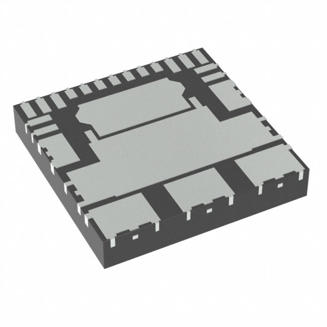


 工商网监
湘ICP备2023018690号
工商网监
湘ICP备2023018690号
