Freescale Semiconductor, Inc.
MOTOROLA
Order Number: MC100ES6254/D
Rev. 3, 05/2004
SEMICONDUCTOR TECHNICAL DATA
Freescale Semiconductor, Inc...
2.5/3.3V Differential LVPECL
2x2 Clock Switch and
Fanout Buffer
The Motorola MC100ES6254 is a bipolar monolithic differential 2x2 clock
switch and fanout buffer. Designed for most demanding clock distribution systems, the MC100ES6254 supports various applications that require to drive precisely aligned clock signals. The device is capable of driving and switching differential LVPECL signals. Using SiGe technology and a fully differential architecture, the device offers superior digital signal characteristics and very low
clock skew error. Target applications for this clock driver are high performance
clock/data switching, clock distribution or data loopback in computing, networking and telecommunication systems.
MC100ES6254
2.5/3.3 V DIFFERENTIAL
LVPECL 2x2
CLOCK SWITCH
AND FANOUT BUFFER
Features:
• Fully differential architecture from input to all outputs
• SiGe technology supports near-zero output skew
•
•
•
•
Supports DC to 3GHz operation1 of clock or data signals
LVPECL compatible differential clock inputs and outputs
LVCMOS compatible control inputs
Single 3.3 V or 2.5 V supply
• 50 ps maximum device skew1
• Synchronous output enable eliminating output runt pulse generation and
metastability
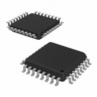
• Standard 32 lead LQFP package
• Industrial temperature range
FA SUFFIX
32-LEAD LQFP PACKAGE
CASE 873A
Functional Description
MC100ES6254 is designed for very skew critical differential clock distribution systems and supports clock frequencies from DC
up to 3.0 GHz. Typical applications for the MC100ES6254 are primary clock distribution, switching and loopback systems of
high-performance computer, networking and telecommunication systems, as well as on-board clocking of OC-3, OC-12 and OC-48
speed communication systems. Primary purpose of the MC100ES6254 is high-speed clock switching applications. In addition, the
MC100ES6254 can be configured as single 1:6 or dual 1:3 LVPECL fanout buffer for clock signals, or as loopback device in highspeed data applications.
The MC100ES6254 can be operated from a 3.3 V or 2.5 V positive supply without the requirement of a negative supply line.
1
The device is functional up to 3 GHz and characterized up to 2.7 GHz.
REV 3
© Motorola, Inc. 2004
For More Information On This Product,
Go to: www.freescale.com
�Freescale Semiconductor, Inc.
MC100ES6254/D
VCC
Bank A
CLK0
CLK0
0
QA1
QA1
QA2
QA2
1
VCC
Bank B
CLK1
CLK1
0
1
Freescale Semiconductor, Inc...
SEL0
SEL1
OEA
OEB
QA0
QA0
QB0
QB0
QB1
QB1
QB2
QB2
Sync
VCC
GND
OEA
CLK0
CLK0
SEL0
GND
VCC
Figure 1. MC100ES6254 Logic Diagram
24
23
22
21
20
19
18
17
QA2
25
16
QB2
QA2
26
15
QB2
VCC
27
14
VCC
QA1
28
13
QB1
MC100ES6254
QA0
31
10
QB0
QA0
32
9
QB0
1
2
3
4
5
6
7
8
VCC
VCC
GND
11
OEB
30
CLK1
VCC
CLK1
QB1
SEL1
12
GND
29
VCC
QA1
Figure 2. 32-Lead Package Pinout (Top View)
2
For More Information On This Product,
Go to: www.freescale.com
TIMING SOLUTIONS
�Freescale Semiconductor, Inc.
MC100ES6254/D
Table 1. PIN CONFIGURATION
Freescale Semiconductor, Inc...
Pin
I/O
CLK0, CLK0
Input
Type
Function
LVPECL
Differential reference clock signal input 0
CLK1, CLK1
Input
LVPECL
Differential reference clock signal input 1
OEA, OEB
Input
LVCMOS
Output enable
SEL0, SEL1
Input
LVCMOS
Clock switch select
QA[0-2], QA[0-2]
QB[0-2], QB[0-2]
Output
LVPECL
Differential clock outputs (banks A and B)
GND
Supply
GND
Negative power supply
VCC
Supply
VCC
Positive power supply. All VCC pins must be connected to the positive power supply for correct
DC and AC operation
Table 2. FUNCTION TABLE
Control
Default
0
1
OEA
0
QA[0-2], Qx[0-2] are active. Deassertion of OE can be QA[0-2] = L, QA[0-2] = H (outputs disabled). Assertion
asynchronous to the reference clock without generation of OE can be asynchronous to the reference clock
of output runt pulses
without generation of output runt pulses
OEB
0
QA[0-2], Qx[0-2] are active. Deassertion of OE can be QA[0-2] = L, QA[0-2] = H (outputs disabled). Assertion
asynchronous to the reference clock without generation of OE can be asynchronous to the reference clock
of output runt pulses
without generation of output runt pulses
00
Refer to Table 3
SEL0, SEL1
Table 3. CLOCK SELECT CONTROL
SEL0
SEL1
CLK0 routed to
CLK1 routed to
Application Mode
0
0
QA[0:2] and QB[0:2]
---
1:6 fanout of CLK0
0
1
---
QA[0:2] and QB[0:2]
1:6 fanout of CLK1
1
0
QA[0:2]
QB[0:2]
Dual 1:3 buffer
1
1
QB[0:2]
QA[0:2]
Dual 1:3 buffer (crossed)
Table 4. ABSOLUTE MAXIMUM RATINGSa
Symbol
Min
Max
Unit
-0.3
3.6
V
-0.3
VCC+0.3
V
-0.3
VCC+0.3
V
DC Input Current
±20
mA
DC Output Current
±50
mA
125
°C
Supply Voltage
VIN
DC Input Voltage
DC Output Voltage
VOUT
IIN
IOUT
TS
a.
Characteristics
VCC
Storage temperature
-65
Condition
Absolute maximum continuous ratings are those maximum values beyond which damage to the device may occur. Exposure to these conditions
or conditions beyond those indicated may adversely affect device reliability. Functional operation at absolute-maximum-rated conditions is not
implied.
TIMING SOLUTIONS
For More Information On This Product,
Go to: www.freescale.com
3
�Freescale Semiconductor, Inc.
MC100ES6254/D
Table 5. GENERAL SPECIFICATIONS
Symbol
VTT
Characteristics
Min
Typ
Unit
MM
ESD Protection (Machine model)
200
V
ESD Protection (Human body model)
2000
V
ESD Protection (Charged device model)
1500
V
Latch-up immunity
200
mA
LU
CIN
θJA
4.0
Thermal resistance junction to ambient
JESD 51-3, single layer test board
JESD 51-6, 2S2P multilayer test board
θJC
Thermal resistance junction to case
Functional temperature range
pF
Inputs
83.1
73.3
68.9
63.8
57.4
86.0
75.4
70.9
65.3
59.6
°C/W
°C/W
°C/W
°C/W
°C/W
Natural convection
100 ft/min
200 ft/min
400 ft/min
800 ft/min
59.0
54.4
52.5
50.4
47.8
60.6
55.7
53.8
51.5
48.8
°C/W
°C/W
°C/W
°C/W
°C/W
Natural convection
100 ft/min
200 ft/min
400 ft/min
800 ft/min
23.0
26.3
°C/W
MIL-SPEC 883E
110
°C
TJ=+110
°C
Operating junction temperatureb
(continuous operation)
MTBF = 9.1 years
TFunc
Condition
V
HBM
CDM
Freescale Semiconductor, Inc...
Max
VCC - 2a
Output termination voltage
TA=-40
Method 1012.1
a.
Output termination voltage VTT=0 V for VCC=2.5 V operation is supported but the power consumption of the device will increase.
b.
Operating junction temperature impacts device life time. Maximum continuous operating junction temperature should be selected according to
the application life time requirements (See application note AN1545 and the application section in this data sheet for more information). The
device AC and DC parameters are specified up to 110°C junction temperature allowing the MC100ES6254 to be used in applications requiring
industrial temperature range. It is recommended that users of the MC100ES6254 employ thermal modeling analysis to assist in applying the
junction temperature specifications to their particular application.
Table 6. DC CHARACTERISTICS (VCC = 3.3 V ± 5% or 2.5 V ± 5%, TJ = 0° to +110°C)
Symbol
Characteristics
Min
Typ
Max
Unit
Condition
0.8
V
±100
µA
VIN=VCC or VIN=GND
LVCMOS control inputs (OEA, OEB, SEL0, SEL1)
VIL
Input voltage low
VIH
Input voltage high
IIN
Input Currenta
2.0
V
LVPECL clock inputs (CLK0, CLK0, CLK1, CLK1)
VPP
VCMR
AC differential input voltageb
0.1
1.3
V
Differential operation
Differential cross point voltagec
1.0
VCC-0.3
V
Differential operation
LVPECL clock outputs (QA0-2, QA0-2, QB0-2, QB0-2)
a.
VOH
Output High Voltage
VOL
Output Low Voltage
IGND
Maximum Quiescent Supply Current
without output termination current
VCC=3.3 V ±5%
VCC=2.5 V ±5%
VCC-1.2
VCC-1.005
VCC-0.7
V
IOH = -30 mAd
VCC-1.9
VCC-1.9
VCC-1.705
VCC-1.705
VCC-1.5
VCC-1.3
V
IOL = -5 mAe
52
85
mA
GND pin
Input have internal pullup/pulldown resistors that affect the input current.
b.
VPP is the minimum differential input voltage swing required to maintain AC characteristic.
c.
VCMR (DC) is the crosspoint of the differential input signal. Functional operation is obtained when the crosspoint is within the VCMR (DC) range
and the input swing lies within the VPP (DC) specification.
d.
Equivalent to a termination 50 Ω to VTT.
e.
ICC calculation:
4
ICC = (number of differential output pairs used) * (IOH + IOL) + IGND
ICC = (number of differential output pairs used) * (VOH-VTT)÷Rload +(VOL-VTT)÷Rload) + IGND
For More Information On This Product,
Go to: www.freescale.com
TIMING SOLUTIONS
�Freescale Semiconductor, Inc.
MC100ES6254/D
Table 7. AC CHARACTERISTICS (VCC = 3.3 V ± 5% or 2.5 V ± 5%, TJ = 0° to +110°C)a
Symbol
VPP
VCMR
Freescale Semiconductor, Inc...
VO(P-P)
Characteristics
Min
Differential input voltageb (peak-to-peak)
0.3
Differential input crosspoint voltagec
1.2
Differential output voltage (peak-to-peak)
fO < 1.1 GHz
fO < 2.5 GHz
fO < 3.0 GHz
fCLK
Input Frequency
tPD
Propagation delay CLK, 1 to QA[] or QB[]
Typ
Max
Unit
1.3
V
VCC-0.3
0
485
3000d
MHz
610
ps
Differential
tsk(O)
Output-to-output skew
50
ps
Differential
tsk(PP)
Output-to-output skew(part-to-part)
250
ps
Differential
tSK(P)
Output pulse skewe
60
ps
DCO
Output duty cycle
tREF < 100 MHz
tREF < 800 MHz
49.4
45.2
50.6
54.8
%
%
DCfref = 50%
DCfref = 50%
Output cycle-to-cycle jitter
RMS (1 σ)
1
ps
SEL0 ≠ SEL1
0.05
300
ps
20% to 80%
tJIT(CC)
360
V
V
V
V
0.7
0.55
0.35
0.45
0.35
0.20
Condition
tr , tf
Output Rise/Fall Time
tPDLf
Output disable time
2.5⋅T + tPD
3.5⋅T + tPD
ns
T = CLK period
tPLDg
Output enable time
3⋅T + tPD
4⋅T + tPD
ns
T = CLK period
a.
AC characteristics apply for parallel output termination of 50 Ω to VTT.
b.
VPP is the minimum differential input voltage swing required to maintain AC characteristics including tpd and device-to-device skew.
c.
VCMR (AC) is the crosspoint of the differential input signal. Normal AC operation is obtained when the crosspoint is within the VCMR (AC) range
and the input swing lies within the VPP (AC) specification. Violation of VCMR (AC) or VPP (AC) impacts the device propagation delay, device and
part-to-part skew.
d.
The MC100ES6254 is fully operational up to 3.0 GHz and is characterized up to 2.7 GHz.
e.
Output pulse skew is the absolute difference of the propagation delay times: | tPLH - tPHL |.
f.
Propagation delay OE deassertion to differential output disabled (differential low: true output low, complementary output high).
g.
Propagation delay OE assertion to output enabled (active).
CLKX
CLKX
50%
OEX
tPDL (OEX to Qx[])
tPLD (OEX to Qx[])
Qx[]
Outputs disabled
Qx[]
Figure 3. MC100ES6254 output disable/enable timing
Differential
Pulse Generator
Z = 50 Ω
ZO = 50 Ω
RT = 50 Ω
ZO = 50 Ω
DUT
MC100ES62
RT = 50 Ω
VTT
VTT
Figure 4. MC100ES6254 AC test reference
TIMING SOLUTIONS
For More Information On This Product,
Go to: www.freescale.com
5
�Freescale Semiconductor, Inc.
MC100ES6254/D
APPLICATIONS INFORMATION
Example Configurations
2x2 clock switch
System A
CLK0
CLK1
3
SEL0
SEL1
System B
3
MC100ES6254
Freescale Semiconductor, Inc...
SEL0 SEL1
Switch configuration
0
0
CLK0 clocks system A and system B
0
1
CLK1 clocks system A and system B
1
0
1
1
CLK0 clocks system A and CLK1 clocks system B
CLK1 clocks system B and CLK1 clocks system A
1:6 Clock Fanout Buffer
CLK0
CLK1
0
0
SEL0
SEL1
MC100ES6254
Understanding the junction temperature range of the
MC100ES6254
To make the optimum use of high clock frequency and low
skew capabilities of the MC100ES6254, the MC100ES6254 is
specified, characterized and tested for the junction temperature
range of TJ=0°C to +110°C. Because the exact thermal performance depends on the PCB type, design, thermal management
and natural or forced air convection, the junction temperature
provides an exact way to correlate the application specific conditions to the published performance data of this data sheet.
The correlation of the junction temperature range to the application ambient temperature range and vice versa can be done
by calculation:
TJ = TA + Rthja ⋅ Ptot
Assuming a thermal resistance (junction to ambient) of
54.4°C/W (2s2p board, 200 ft/min airflow, refer to table 4) and
a typical power consumption of 467 mW (all outputs terminated
50 Ω to VTT, VCC=3.3 V, frequency independent), the junction
temperature of the MC100ES6254 is approximately
TA + 24.5°C, and the minimum ambient temperature in this example case calculates to -24.5°C (the maximum ambient temperature is 85.5°C. Refer to Table 8). Exceeding the minimum
junction temperature specification of the MC100ES6254 does
not have a significant impact on the device functionality. However, the continuous use the MC100ES6254 at high ambient
temperatures requires thermal management to not exceed the
specified maximum junction temperature. Refer to the Application Note AN1545 for a power consumption calculation guideline.
Table 8. Ambient temperature ranges (Ptot = 467 mW)
Loopback device
Rthja (2s2p board)
System-Tx
CLK0
QA[]
Transmitter
SEL0
SEL1
System-Rx
QB[]
CLK1
Receiver
MC100ES6254
6
a.
SEL0
SEL1
Switch configuration
0
0
System loopback
0
1
Line loopback
1
0
Transmit / Receive operation
1
1
System and line loopback
TA, mina
TA, max
-28°C
82°C
Natural convection
59.0°C/W
100 ft/min
54.4°C/W
-25°C
85°C
200 ft/min
52.5°C/W
-24.5°C
85.5°C
400 ft/min
50.4°C/W
-23.5°C
86.5°C
800 ft/min
47.8°C/W
-22°C
88°C
The MC100ES6254 device function is guaranteed from TA=-40°C
to TJ=110°C
Maintaining Lowest Device Skew
The MC100ES6254 guarantees low output-to-output bank
skew of 50 ps and a part-to-part skew of maximum 250 ps. To
ensure low skew clock signals in the application, both outputs
of any differential output pair need to be terminated identically,
even if only one output is used. When fewer than all nine output
pairs are used, identical termination of all output pairs within the
output bank is recommended. If an entire output bank is not
used, it is recommended to leave all of these outputs open and
unterminated. This will reduce the device power consumption
while maintaining minimum output skew.
For More Information On This Product,
Go to: www.freescale.com
TIMING SOLUTIONS
�Freescale Semiconductor, Inc.
MC100ES6254/D
VCC
VCC
33...100 nF
0.1 nF
MC100ES6254
Figure 5. VCC Power Supply Bypass
Freescale Semiconductor, Inc...
Power Supply Bypassing
The MC100ES6254 is a mixed analog/digital product. The
differential architecture of the MC100ES6254 supports low
noise signal operation at high frequencies. In order to maintain
its superior signal quality, all VCC pins should be bypassed by
high-frequency ceramic capacitors connected to GND. If the
spectral frequencies of the internally generated switching noise
on the supply pins cross the series resonant point of an individual bypass capacitor, its overall impedance begins to look inductive and thus increases with increasing frequency. The parallel capacitor combination shown ensures that a low impedance path to ground exists for frequencies well above the noise
bandwidth.
TIMING SOLUTIONS
For More Information On This Product,
Go to: www.freescale.com
7
�Freescale Semiconductor, Inc.
MC100ES6254/D
OUTLINE DIMENSIONS
4X
0.20 H
6
A-B D
D1
PIN 1 INDEX
3
e/2
D1/2
32
A, B, D
25
1
E1/2 A
F
B
6 E1
E
4
F
DETAIL G
Freescale Semiconductor, Inc...
8
17
9
7
NOTES:
1. DIMENSIONS ARE IN MILLIMETERS.
2. INTERPRET DIMENSIONS AND TOLERANCES PER
ASME Y14.5M, 1994.
3. DATUMS A, B, AND D TO BE DETERMINED AT
DATUM PLANE H.
4. DIMENSIONS D AND E TO BE DETERMINED AT
SEATING PLANE C.
5. DIMENSION b DOES NOT INCLUDE DAMBAR
PROTRUSION. ALLOWABLE DAMBAR PROTRUSION
SHALL NOT CAUSE THE LEAD WIDTH TO EXCEED
THE MAXIMUM b DIMENSION BY MORE THAN
0.08-mm. DAMBAR CANNOT BE LOCATED ON THE
LOWER RADIUS OR THE FOOT. MINIMUM SPACE
BETWEEN PROTRUSION AND ADJACENT LEAD OR
PROTRUSION: 0.07-mm.
6. DIMENSIONS D1 AND E1 DO NOT INCLUDE MOLD
PROTRUSION. ALLOWABLE PROTRUSION IS
0.25-mm PER SIDE. D1 AND E1 ARE MAXIMUM
PLASTIC BODY SIZE DIMENSIONS INCLUDING
MOLD MISMATCH.
7. EXACT SHAPE OF EACH CORNER IS OPTIONAL.
8. THESE DIMENSIONS APPLY TO THE FLAT
SECTION OF THE LEAD BETWEEN 0.1-mm AND
0.25-mm FROM THE LEAD TIP.
4
D
4X
A-B D
H
SEATING
PLANE
DETAIL G
D
D/2
0.20 C
E/2
28X
e
32X
C
0.1 C
DETAIL AD
PLATING
BASE
METAL
b1
c
c1
b
8X
(θ1˚)
0.20
R R2
A2
C A-B D
SECTION F-F
R R1
A
M
5
0.25
GAUGE PLANE
A1
(S)
L
(L1)
θ˚
DETAIL AD
8
DIM
A
A1
A2
b
b1
c
c1
D
D1
e
E
E1
L
L1
q
q1
R1
R2
S
FA SUFFIX
CASE 873A-03
ISSUE
B
LQFP PACKAGE
CASE 873A-02
ISSUE B
8
For More Information On This Product,
Go to: www.freescale.com
MILLIMETERS
MIN
MAX
1.40
1.60
0.05
0.15
1.35
1.45
0.30
0.45
0.30
0.40
0.09
0.20
0.09
0.16
9.00 BSC
7.00 BSC
0.80 BSC
9.00 BSC
7.00 BSC
0.50
0.70
1.00 REF
0˚
7˚
12 REF
0.08
0.20
0.08
--0.20 REF
DATE 03/10/00
TIMING SOLUTIONS
�Freescale Semiconductor, Inc.
MC100ES6254/D
Freescale Semiconductor, Inc...
NOTES
TIMING SOLUTIONS
For More Information On This Product,
Go to: www.freescale.com
9
�Freescale Semiconductor, Inc.
MC100ES6254/D
Freescale Semiconductor, Inc...
NOTES
10
For More Information On This Product,
Go to: www.freescale.com
TIMING SOLUTIONS
�Freescale Semiconductor, Inc.
MC100ES6254/D
Freescale Semiconductor, Inc...
NOTES
TIMING SOLUTIONS
For More Information On This Product,
Go to: www.freescale.com
11
�Freescale Semiconductor, Inc...
Freescale Semiconductor, Inc.
Information in this document is provided solely to enable system and software implementers to use Motorola products. There are no express or implied
copyright licenses granted hereunder to design or fabricate any integrated circuits or integrated circuits based on the information in this document.
Motorola reserves the right to make changes without further notice to any products herein. Motorola makes no warranty, representation or guarantee
regarding the suitability of its products for any particular purpose, nor does Motorola assume any liability arising out of the application or use of any product
or circuit, and specifically disclaims any and all liability, including without limitation consequential or incidental damages. “Typical” parameters which may be
provided in Motorola data sheets and/or specifications can and do vary in different applications and actual performance may vary over time. All operating
parameters, including “Typicals” must be validated for each customer application by customer’s technical experts. Motorola does not convey any license
under its patent rights nor the rights of others. Motorola products are not designed, intended, or authorized for use as components in systems intended for
surgical implant into the body, or other applications intended to support or sustain life, or for any other application in which the failure of the Motorola product
could create a situation where personal injury or death may occur. Should Buyer purchase or use Motorola products for any such unintended or
unauthorized application, Buyer shall indemnify and hold Motorola and its officers, employees, subsidiaries, affiliates, and distributors harmless against all
claims, costs, damages, and expenses, and reasonable attorney fees arising out of, directly or indirectly, any claim of personal injury or death associated
with such unintended or unauthorized use, even if such claim alleges that Motorola was negligent regarding the design or manufacture of the part.
MOTOROLA and the Stylized M Logo are registered in the US Patent and Trademark Office. All other product or service names are the property of their
respective owners.
© Motorola, Inc. 2004
HOW TO REACH US:
USA/EUROPE/LOCATIONS NOT LISTED:
Motorola Literature Distribution
P.O. Box 5405, Denver, Colorado 80217
1-800-521-6274 or 480-768-2130
JAPAN: Motorola Japan Ltd.; SPS, Technical Information Center
3-20-1 Minami-Azabu. Minato-ku, Tokyo 106-8573, Japan
81-3-3440-3569
ASIA/PACIFIC: Motorola Semiconductors H.K. Ltd.; Silicon Harbour Centre
2 Dai King Street, Tai Po Industrial Estate, Tai Po, N.T., Hong Kong
852-26668334
HOME PAGE: http://motorola.com/semiconductors
For More Information On This Product,
Go to: www.freescale.com
MC100ES6254/D
�


 工商网监
湘ICP备2023018690号
工商网监
湘ICP备2023018690号
