Freescale Semiconductor
Advance Information
Document Number: MC34929
Rev. 7.0, 11/2006
Brushless DC 1.0 AMP 28 VOLT
Motor Driver IC
The 34929 Brushless DC (BLDC) Motor Driver IC is a complete
BLDC motor driver system in one chip. It is designed to efficiently drive
three-phase BLDC motors up to 1A and 28V, and has built in protection
features making it ideal for a variety of consumer, portable, and office
applications containing small motors. It incorporates digital I/O, making
it easy to use with an MCU in a closed-loop motor control system. It has
a built-in Hall-effect sensors interface and a Hall sensors voltage
supply, so it can operate BLDC motors as a stand-alone controller/
driver. Its sophisticated analog/mixed-signal state machine
accommodates several modes of operation, including: Forward (CW),
Reverse (CCW), Run/Stop, Braking, Variable Speed (External PWM),
and Torque Limit (maximum-current-limit) modes.
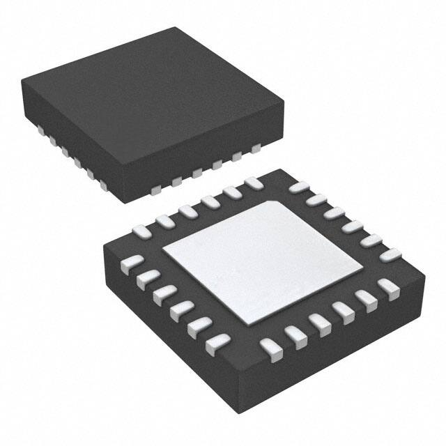
34929
BRUSHLESS DC MOTOR DRIVER
QFN SUFFIX
98ARH99033A
24-PIN QFN (4X4X1)
Features
•
•
•
•
•
•
•
•
•
•
Single-Supply Operation (8V–28V)
Built-in Hall Sensors Controlled-Supply (VH)
3-Phase Hall Sensors Interface
Two Tachometer Outputs (1X and 3X Hall Frequency)
Adjustable Maximum Current Limit (Torque Limiting)
Adjustable Stalled Rotor Detection and Protection
Short Circuit Detection and Protection
Over-Temperature Detection and Thermal Shutdown
Undervoltage Detection and Shutdown
Pb-Free Packaging Designated by Suffix Code EP.
CP
ORDERING INFORMATION
PWM
TACH
-0°C to 85°C
24 QFN
ISENS
PGND
CT
GND
MC34929EP
LSS
DIR
3XTACH
Package
CRES V+
PHC
PHB
PHA
RUN
MCU
Temperature
Range (TA)
V+
34929
CP+ CP-
Device
VH
HAB+
HABHBC+
HBCHCA+
HCA-
Figure 1. 34929 Simplified Application Diagram
* This document contains certain information on a new product.
Specifications and information herein are subject to change without notice.
© Freescale Semiconductor, Inc., 2006. All rights reserved.
BDLC
MOTOR
�INTERNAL BLOCK DIAGRAM
INTERNAL BLOCK DIAGRAM
CP+
CP-
CRES
V+
Charge
Pump
V+
Q1
VGHS
Q3
Q5
High Side
Gate Drive
VDD
V Ref
PHC
PHB
Regs &
V Ref
SC Det
Q2
Q4
Q6
PHA
Low Side
Gate Drive
LSS
ISENS
ILIM
PGND
UVLO
VH
TLIM
V
O
HAB+
HAB
G
HAB-
Control
Logic
V5V
HBC+
HBC
PWM
RUN
V5V
DIR
CT
HBC-
V5V
HCA
VCC
HCA+
HCA-
Input
Protection
Stall
Det
3XTACH
TACH
GND
Figure 2. 34929 Simplified Internal Block Diagram
34929
2
Analog Integrated Circuit Device Data
Freescale Semiconductor
�PIN CONNECTIONS
6
12
VH
5
11
PHC
4
10
PHA
3
V+
9
LSS
2
GND
CP-
8
PHB
1
CT
CP+
7
ISENS
13
HAB+
23
PWM
14
HAB-
22
PGND
15
HBC+
21
DIR
16
HBC-
20
3XTACH
17
HCA+
19
TACH
18
HCA-
RUN
24
PIN CONNECTIONS
CRES
Figure 3. 34929 Pin Connections
Table 1. 34929 Pin Definitions
Pin Number
Pin Name
Pin Function
Formal Name
Definition
1
HCA-
INPUT
HALL CA NEG
RECEIVES NEGATIVE OUTPUT FROM SENSOR LOCATED
BETWEEN ‘C’ AND ‘A’ PHASES
2
HCA+
INPUT
HALL CA POS
RECEIVES POSITIVE OUTPUT FROM SENSOR LOCATED
BETWEEN ‘C’ AND ‘A’ PHASES
3
HBC-
INPUT
HALL BC NEG
RECEIVES NEGATIVE OUTPUT FROM SENSOR LOCATED
BETWEEN ‘B’ AND ‘C’ PHASES
4
HBC+
INPUT
HALL BC POS
RECEIVES POSITIVE OUTPUT FROM SENSOR LOCATED
BETWEEN ‘B’ AND ‘C’ PHASES
5
HAB-
INPUT
HALL AB NEG
RECEIVES NEGATIVE OUTPUT FROM SENSOR LOCATED
BETWEEN ‘A’ AND ‘B’ PHASES
6
HAB+
INPUT
HALL AB POS
RECEIVES POSITIVE OUTPUT FROM SENSOR LOCATED
BETWEEN ‘A’ AND ‘B’ PHASES
7
CRES
COMPONENT
RESERVOIR CAP
EXTERNAL CHARGE PUMP RESEVOIR CAP
8
CP+
COMPONENT
CHARGE PUMP POS
POSITIVE SIDE OF CHARGE PUMPING CAP
9
CP-
COMPONENT
CHARGE PUMP NEG
NEGATIVE SIDE OF CHARGE PUMPING CAP
10
V+
SUPPLY
POSITIVE SUPPLY
MAIN SUPPLY INPUT FOR DEVICE AND MOTOR
23
PGND
RETURN
POWER GROUND
POWER GROUND
12
CT
COMPONENT
TIMING CAP
13
VH
OUTPUT
HALL VOLTAGE
SUPPLY VOLTAGE FOR THE EXTERNAL HALL SENSORS
14
PHC
OUTPUT
PHASE C OUTPUT
HALF BRIDGE OUTPUT FOR PHASE “C” MOTOR WINDING
15
PHA
OUTPUT
PHASE A OUTPUT
HALF BRIDGE OUTPUT FOR PHASE “A” MOTOR WINDING
16
LSS
RETURN
17
PHB
OUTPUT
EXTERNAL CAP FOR STALL DETECT TIMING
LOW SIDE SOURCES COMMON SOURCE PIN FOR LOWER HALF OF BRIDGE
PHASE B OUTPUT
HALF BRIDGE OUTPUT FOR PHASE “B” MOTOR WINDING
34929
Analog Integrated Circuit Device Data
Freescale Semiconductor
3
�PIN CONNECTIONS
Table 1. 34929 Pin Definitions (continued)
Pin Number
Pin Name
Pin Function
Formal Name
Definition
19
RUN
INPUT
RUN
RUN/STOP CONTROL INPUT (ACTIVE LOW = MOTOR RUNNING)
20
TACH
OUTPUT
TACH OUTPUT
21
3XTACH
OUTPUT
3X TACH OUTPUT
OPEN-DRAIN-BUFFERED, EXOR’ED OUTPUT OF ALL THREE
SENSORS
22
DIR
INPUT
DIRECTION
DIRECTION CONTROL INPUT (ACTIVE LOW = CW ROTATION)
11
GND
RETURN
SIGNAL GROUND
SIGNAL GROUND FOR DEVICE
24
PWM
INPUT
PWM OR ENABLE
PWM SIGNAL INPUT (ACTIVE LOW = OUTPUTS ENABLED)
18
ISENS
INPUT
CURRENT SENSE
CURRENT LIMITING SENSE RESISTOR INPUT
OPEN-DRAIN-BUFFERED OUTPUT OF SENSOR ‘AB’
34929
4
Analog Integrated Circuit Device Data
Freescale Semiconductor
�ELECTRICAL CHARACTERISTICS
MAXIMUM RATINGS
ELECTRICAL CHARACTERISTICS
MAXIMUM RATINGS
Table 2. Maximum Ratings
All voltages are with respect to ground. Exceeding these ratings may cause a malfunction or permanent damage to the device.
Ratings
Symbol
Value
Unit
V+TRANS
42
V
VI/O
-0.6 to 5.5
V
TACHOUT
42
V
IO(CONT)
1.0
A
IO(PK)
1.5
A
Bridge Output Voltage
VO
-1.0 to (V+) +1.0
V
Hall Voltage Supply Current
IVH
30
mA
ELECTRICAL RATINGS
Power Supply Transient Voltage
Signal I/O Pins
Open Drain Outputs (TACH and 3XTACH)
Bridge Output Continuous Current
Bridge Output Peak Current
ESD Voltage (1)
V
VESD
Human Body Model (HBM)
2000
Machine Model (MM)
200
THERMAL RATINGS
Operating Ambient Temperature
TA
-0 to 85
°C
Maximum Junction Temperature
TJ-MAX
150
°C
TSTG
-0 to 150
°C
RθJA
9 cm2.
With specified PCB Layout shown in Figure 4 under forced convection airflow condition.
Pin soldering temperature limit is for 10 seconds maximum duration. Not designed for immersion soldering. Exceeding these limits may
cause malfunction or permanent damage to the device.
Freescale’s Package Reflow capability meets Pb-free requirements for JEDEC standard J-STD-020C. For Peak Package Reflow
Temperature and Moisture Sensitivity Levels (MSL),
> Go to www.freescale.com
> Search by part number [e.g. remove prefixes/suffixes and enter the core ID to view all orderable parts. (i.e. MC33xxxD enter 33xxx)]
> Locate your Part Number and in the Details column, select “View”
> Select “Environmental and Compliance Information”
Figure 4. Printed Circuit Board Layout for Maximum Thermal Performance
34929
Analog Integrated Circuit Device Data
Freescale Semiconductor
5
�ELECTRICAL CHARACTERISTICS
STATIC ELECTRICAL CHARACTERISTICS
STATIC ELECTRICAL CHARACTERISTICS
Table 3. Static Electrical Characteristics
Characteristics noted under conditions 8.0 V ≤ VSUP ≤ 28 V, - 0°C ≤ TA ≤ 85°C, GND = 0 V unless otherwise noted. Typical
values noted reflect the approximate parameter means at TA = 25°C under nominal conditions unless otherwise noted.
Characteristic
Symbol
Min
Typ
Max
Unit
V+
8.0
12
28
V
ISA
—
2.0
3.0
mA
IQ
—
4.0
6.0
mA
V+-LV
5.0
5.5
6.0
V
VLV-HYS
—
100
—
mV
VIL
—
—
0.8
V
VIH
2.0
—
—
V
VI-HYS
50
300
—
mV
IIL
—
-50
—
µA
RPULLUP
—
100
—
kΩ
VH-SENS
50
—
—
mV
VH-CMM
0.0
—
3.0
V
VH-HYS
—
15
—
mV
IH
-10
—
10
µA
Charge Pump Output Voltage
VGHS
—
—
(V+) +12
V
Charge Pump Reservoir Capacitor
CCRES
—
0.1
—
µF
CCP
—
0.1
—
µF
VOL
—
—
0.4
V
IOH
—
—
10
µA
VH
—
—
(V+) -1.0
V
Power Supply Voltage Range
Suspend Power Supply Current
(6)
Operation Power Supply Current
(7)
Low V+ Detect Voltage
Low V+ Detect Hysteresis
Logic Inputs Threshold Low
(8)
Logic Inputs Threshold High
(8)
Logic Inputs Hysteresis Voltage
Logic Input Current Low
(8)
(9)
Logic Input Pull-Up Resistance
Hall Inputs Voltage Sensitivity
(10)
(11)
Hall Inputs Common Mode Voltage Range
Hall Inputs Hysteresis Voltage
Hall Input Current
(11)
(11)
(11)
Charge Pump Capacitor
Logic Output Voltage Low
(12)
Logic Output Leakage Current High
Hall Sensors Supply
Notes
6.
7.
8.
9.
10.
11.
12.
(13)
Voltage(14)
With device in suspend mode (RUN command = False).
The current consumed internal to the IC, but not including current output for motor drive.
PWM, RUN, and DIR pins.
PWM, RUN, and DIR pins with R-pullup = 100 kΩ.
Internal Pullup resistance value can vary by 20%.
HCA-, HCA+, HBC-, HBC+, HAB-, HAB+ pins.
TACH and 3XTACH pins @ IOL = 5.0 mA.
13.
TACH and 3XTACH pins @ VOH = 24 V.
14.
VH pin @ Io-hall = 10 mA.
34929
6
Analog Integrated Circuit Device Data
Freescale Semiconductor
�ELECTRICAL CHARACTERISTICS
STATIC ELECTRICAL CHARACTERISTICS
Table 3. Static Electrical Characteristics (continued)
Characteristics noted under conditions 8.0 V ≤ VSUP ≤ 28 V, - 0°C ≤ TA ≤ 85°C, GND = 0 V unless otherwise noted. Typical
values noted reflect the approximate parameter means at TA = 25°C under nominal conditions unless otherwise noted.
Characteristic
Symbol
Min
Typ
Max
Unit
RON-T
—
0.25
0.5
Ω
RON-B
—
0.25
0.5
Ω
RON-T_REF
—
0.3
0.6
Ω
RON-B_REF
—
0.3
0.6
Ω
VF-LD
—
1.2
—
V
IO-LDC
—
128
—
µA
Stall Detection Timer Detection Voltage
V-CTDET
—
2.5
—
V
Current Limit Sense Voltage Threshold
VISENS
0.09
0.1
0.11
V
TSD
150
165
180
°C
TSD-HYS
—
30
—
°C
High Side RDS-ON (15)
Low Side RDS-ON
(15)
High Side RDS-ON (hot)
(16)
Low Side RDS-ON (hot)
(16)
H-bridge MOSFETs’ Body-Diode Forward Voltage Drop
Stall Detection Timer Output Current
(17)
Thermal Shutdown Temperature
TSD Hysteresis
Notes
15. @ TA = 25°C, 14 V =< V+ =< 28 V, IO = 1.0 A.
16.
Typical value (for reference only) @ 85°C =< TJ =< 150°C, 8.0 V =< V+ =< 14 V. Not tested; not guaranteed.
17.
@ IF = 1.0 A for each output MOSFET (measured from source to drain).
34929
Analog Integrated Circuit Device Data
Freescale Semiconductor
7
�ELECTRICAL CHARACTERISTICS
DYNAMIC ELECRTICAL CHARACTERISTICS
DYNAMIC ELECRTICAL CHARACTERISTICS
Table 4. Dynamic Electrical Characteristics
Characteristics noted under conditions 7.0 V ≤ VSUP ≤ 18 V, - 0°C ≤ TA ≤ 85°C, GND = 0 V unless otherwise noted. Typical
values noted reflect the approximate parameter means at TA = 25°C under nominal conditions unless otherwise noted.
Characteristic
Charge Pump Switching Frequency
Symbol
Min
Typ
Max
Unit
FCP
—
250
—
kHz
High-Side Gate-Drive Supply Wake-Up Time
TWAKE
—
1.0
2.0
ms
Controlled Braking Period
TCBRK
—
20
—
ms
Low V+ Detect Suspend Time
TSPND
—
100
—
µs
Power-On Reset Wait Time
TWAIT
—
1.0
—
ms
Maximum PWM Input Frequency
FPWM
—
—
100
kHz
Propagation Delay Time (18)
TDELAY
—
—
(1.0)
µs
Output Low Side Off Time (Rise) (18)
TLS-OFF
—
(25)
—
ns
Output High Side On Time (Rise) (18)
THS-ON
—
(25)
—
ns
Output High Side Off Time (Fall) (18)
THS-OFF
—
(25)
—
ns
Output Low Side On Time (Fall) (18)
TLS-ON
—
(175)
—
ns
TOFF
—
(100)
—
ns
Shoot Through Prevention Time (Output H-bridge High-Z) (18)
Notes
18. Load condition: Star connected 5.6 Ω load resistances (approximates 1.0 A output current at 12V V+).
34929
8
Analog Integrated Circuit Device Data
Freescale Semiconductor
�ELECTRICAL CHARACTERISTICS
TIMING DIAGRAMS
TIMING DIAGRAMS
RUN
TWAKE
90%
VGHS
Figure 5. High-Side Gate-Drive Supply Wake-Up Time “Twake”
VLV-HYS
V+
V+-LV
TSPND
TWAIT
Reset
(Internal)
Figure 6. Timing for Reset on Low V+ Detect
Reset X
OR
RUN
DIR
HAB
HBC
Stall
HCA
CT
Stall_Detect X
~2 sec @ 0.1 µF
Stall_Protect X
Figure 7. Stall Detection/Protection Timing
34929
Analog Integrated Circuit Device Data
Freescale Semiconductor
9
�ELECTRICAL CHARACTERISTICS
TIMING DIAGRAMS
TOFF
TOFF
HS-ON
LS-OFF
LS-ON
HS-OFF
90%
90%
10%
10%
90%
90%
Output Rise Time = LS-OFFf + HS-ON
Output Fall Time = HS-OFF + LS-ON
10%
10%
Figure 8. Rise Time, Fall Time, Shoot Through Prevention Timing
Controlled
Brake
CW Rotation
Reverse Brake
Stop
CCW Rotation
HAB
HBC
HCA
DIR
TACH
3XTACH
C
B
A
HAB
TCBRK
Figure 9. Controlled Brake Mode Timing
34929
10
Analog Integrated Circuit Device Data
Freescale Semiconductor
�ELECTRICAL CHARACTERISTICS
TIMING DIAGRAMS
Rotation Detection
HAB
HBC
HCA
HAB
HBC
HCA
RST
DIR
Reset
Internal
Reset
Stall Det.
Latch
Stall_Protect
Stall_Detect Counter
Count
Relaxation
Oscillator
RUN
Carry
Reset
Stall_Detect
CT
0.1 µF
Figure 10. Stalled Rotor Detection Logic Diagram
On
Off
Off
Off
On
Off
PWM = Enabled
PWM = Disabled
On
On
Off
Off
Off
Off
Figure 11. Synchronous Rectification “Slow-Decay Current” Example
34929
Analog Integrated Circuit Device Data
Freescale Semiconductor
11
�ELECTRICAL CHARACTERISTICS
TIMING DIAGRAMS
PWM
C
B
A
Figure 12. PWM Switching Waveforms
Figure 13. ISENS Current Limit Waveforms
PWM
TDELAY
Phases
Figure 14. Propagation Delay
34929
12
Analog Integrated Circuit Device Data
Freescale Semiconductor
�FUNCTIONAL DESCRIPTION
INTRODUCTION
FUNCTIONAL DESCRIPTION
INTRODUCTION
The MC34929 Brushless DC Motor Driver IC is a complete
BLDC motor driver system in one chip. It is designed to
efficiently drive three-phase BLDC motors up to 1.0 A and
28 V, and has built in protection features making it ideal for a
variety of consumer and office applications containing small
motors. Because it has a built-in Hall-sensors interface and
Hall sensors bias supply, it can operate motors either standalone (e.g., with pushbutton/switch interface), or under the
control of an external MCU. Its sophisticated analog/mixedsignal state machine accommodates several modes of
operation, including: clockwise, counterclockwise, run/stop,
brake, variable speed (PWM), and torque limit (current limit).
FUNCTIONAL PIN DESCRIPTION
HAL CA NEG (HCA-)
Receives negative output from sensor located between ‘c’
and ‘a’ phases.
TIMING CAP (CT)
External cap for stall detect timing.
HALL VOLTAGE (VH)
HAL CA POS (HCA+)
Receives positive output from sensor located between ‘c’
and ‘a’ phases.
HAL BC NEG (HBC-)
Supply voltage for the external hall sensors.
PHASE C OUTPUT (PHC)
Half bridge output for phase “c” motor winding.
Receives negative output from sensor located between ‘b’
and ‘c’ phases.
PHASE A OUTPUT (PHC)
HAL BC POS (HBC+)
LOW SIDE SOURCES (LSS)
Receives positive output from sensor located between ‘b’
and ‘c’ phases.
HAL AB NEG (HAB-)
Receives negative output from sensor located between ‘a’
and ‘b’ phases.
HAL AB POS (HAB+)
Receives positive output from sensor located between ‘a’
and ‘b’ phases.
Half bridge output for phase “a” motor winding.
Common source pin for lower half of bridge.
PHASE B OUTPUT (PHB)
Half bridge output for phase “b” motor winding.
CURRENT SENSE (ISENS)
Current limiting sense resistor input.
RUN (RUN)
Run/stop control input (active low = motor running).
RESERVOIR CAP (CRES)
External charge pump resevoir cap.
TACH OUTPUT (TACH)
Open-drain-buffered output of sensor ‘ab’.
CHARGE PUMP POS (CP+)
Positive side of charge pumping cap.
3X TACH OUTPUT (3XTACH)
Open-drain-buffered, exor’ed output of all three sensors.
CHARGE PUMP NEG (CP-)
Negative side of charge pumping cap.
DIRECTION (DIR)
Direction control input (active low = cw rotation).
POSITIVE SUPPLY (V+)
Main supply input for device and monitor.
POWER GROUND (PGND)
Power ground.
SIGNAL GROUND (GND)
Signal ground for the device.
PWM OR ENABLE (PWM)
Pwm signal input (active low = outputs enabled).
34929
Analog Integrated Circuit Device Data
Freescale Semiconductor
13
�FUNCTIONAL DEVICE OPERATION
FUNCTIONAL DEVICE OPERATION
The following paragraphs describe the internal function of
the 34929 as shown in Figure 2.
HALL COMPARATORS
The Hall comparators square-up the signals from the Hall
sensors.
CHARGE PUMP
This charge pump provides the VGHS and internal power
supply for the high side power MOSFET gate drive. Its output
voltage is limited to V+ +10V to prevent damage to the driver
circuits or MOSFET gates. However, VGHS will be below V+
+10V if V+ supply voltage is below 12V. The switching
frequency of this charge pump is ~250 kHz. The VGHS
supply wakes up typically 1ms after the RUN command is
initiated.
REGULATORS AND VOLTAGE REFERENCE
Internal regulators provide operating and reference
voltages for use by the analog/mixed-signal circuitry. This
function also includes providing the drive voltage for the lowside gate drivers. The regulators for the internal logic and
analog circuits comprise regulators for the logic circuits, and
regulators for the analog circuits (including input/output
buffering, but excepting the power outputs). A bandgap
circuit generates the internal precision reference voltage
(1.25 V). This is used for biasing the comparators and other
analog circuits. (Note: this reference voltage is not externally
available.)
INTERNAL CLOCK
The internal clock generates a stable pulse-train for use by
the IC’s logic circuits. Its output frequency is 1.0 MHz ±30%.
The clock circuit also includes frequency-dividers to derive
lower frequency pulse trains for use by circuits such as the
charge pump and various internal timers, etc.).
INPUT LOGIC
All logic input pins have internal 100K Ω pull-ups
connected to the internal Vdd logic supply. The logic input
circuitry includes the following inputs:
• PWM input controls the speed of motor. Output = “Enable”
when PWM = “L”, and then Output = “Disable” (means “Z”:
High Impedance) when PWM = “H”.
• RUN input controls the start and stop function. When RUN
= “H”, this IC will go to suspend mode via controlled brake
state and suspend unnecessary circuits (Internal OSC,
Counters, Charge pump, Stall detection and protection).
• DIR input controls the direction of motor. When DIR is
flipped, the motor will be reverse, brake through controlled
brake, and then rotate to reverse direction. This DIR pin
has capability to be applied to V+ + VF.
HALL SWITCH
A high side switch to turn-on and turn-off the Hall supply
current.
TACH, 3XTACH OUTPUT
The TACH outputs are as follows: TACH is the inverted
HAB signal. 3XTACH is from inverted EXOR with all three
Hall sensor signals. These outputs are both open drain type.
LOW V+ DETECT
The low V+ voltage detection circuit monitors V+; if the V+
voltage falls below the threshold, the IC will reset after
TSPND time. This circuitry will not respond to negative-going
transients on V+ within the TSPND time period. Once placed in
suspend mode, V+ must return to a level greater than the
detection threshold plus and additional 100mv (typical)
hysteresis, and stay there for the TWAIT period, before the IC
will come out of suspend mode.
RESET
The reset function works as follows: when an error
condition, such as V+ falling below the V+-LV threshold, is
detected, the IC will be in placed in suspend mode (all output
MOSFETs set to a high impedance state) by way of a
controlled-braking transition state. This will occur regardless
of RUN command status. Note, the error condition must exist
for a time period greater than TSPND before the internal reset
will be generated. When the error condition resolves,
suspend mode will be released after the TWAIT period. (See
Figure 6.)
STALL DETECTION AND PROTECTION
The stall detection and protection circuit actively monitors
operation for a stalled rotor event while the RUN command is
set = “True”. A stall is detected as follows (see Figure 7):
1) A sawtooth waveform generated at the timing capacitor,
TC, is monitored by the stall-detect counter which is counting
the sawtooth cycles.
2) The stall-detect counter is being reset (cleared) every
time there is a transition on any of the outputs from the Hall
comparators (HAB, HBC, or HCA).
3) A “stall condition” is assumed anytime the stall-detect
counter is allowed to overflow, (i.e., anytime the counter is not
cleared back to zero by the EXOR’ed output of the HAB,
HBC, and HCA comparators). This can only occur when at
least two of the signals (HAB, HBC, or HCA) have become
static (fixed to “H” or “L”).
34929
14
Analog Integrated Circuit Device Data
Freescale Semiconductor
�FUNCTIONAL DEVICE OPERATION
CONTROLLED BRAKE MODE
4) Once the internal Stall-Detect signal is asserted, an
internal Stall-Protect signal is latched. The Stall-Protect latch
keeps the IC in suspend-mode even if the stall condition is
subsequently resolved.
5) The Stall-Protect Latch can only be reset by Toggling
V+, RUN or DIR.
The controlled brake mode prevents high Back-EMF
voltages from being created when decelerating the motor to
change direction. When the DIR command changes state, all
three phases are held low for the time period “TCBRK”
(~20 msec @ 500 rpm with a 12-pole rotor). See Figure 12.
PWM CONTROL
SHORT CIRCUIT PROTECTION
The phase outputs can be controlled with a PWM input.
During PWM’ing, the freewheeling currents generated by the
motor’s windings are synchronously rectified by the output Hbridge to produce a slow decay waveform and avoid
dissipating excess power in the IC (see Figure 12).
The short circuit protection function utilizes sense-FETs in
the H-bridge high-side MOSFETs. If a short circuit occurs the
sense-FET portion of the affected high-side MOSFET’s cells
will provide an output to the short-circuit detection circuitry
that exceeds the preset threshold, and the short-circuit
detection circuitry will immediately set all phase output to
LOW (i.e., all low-side MOSFETs will be turned on).
CURRENT LIMIT
The current limit function provides the means to set the
maximum allowed motor current, and thus effectively sets the
maximum possible torque the motor can apply to its load. The
function is implemented via an external sense resistance
RISENSE through which flows the return current of the 3phase H-bridge. The voltage drop across RISENSE is
monitored by the ISENS pin, and whenever the threshold of
0.1V is exceeded, the phase that is currently low will be
brought high. The output will be released ~40 µs later. The
output will then follow the PWM input once again.
THERMAL SHUTDOWN
The thermal shutdown protection function utilizes an onchip temperature sensor and a threshold comparator with
preset hysteresis. If the die temperature exceeds the TSD
temperature threshold, the protection circuitry will
immediately set all phase outputs to OFF (i.e., all H-bridge
MOSFETs will be set to a high-impedance state). Thermal
shutdown reacts to any cause of over-temperature, including
that resulting from prolonged running at high currents with
insufficient cooling.
34929
Analog Integrated Circuit Device Data
Freescale Semiconductor
15
�FUNCTIONAL DEVICE OPERATION
LOGIC COMMANDS AND REGISTERS
LOGIC COMMANDS AND REGISTERS
Table 5. 3 Phase Motor Drive Truth Table
DIR
Hall AB
Hall BC
Hall CA
PWM
C
B
A
TACH
3XTACH
X
L
L
L
X
Z
Z
Z
H
H
X
H
H
H
X
Z
Z
Z
L
L
L
L
L
H
L
Z
H
L
H
H
L
L
H
L
L
H
L
Z
H
H
L
L
H
H
L
H
Z
L
H
L
L
H
L
L
L
L
Z
H
L
H
L
H
L
H
L
L
H
Z
L
L
L
H
H
L
L
Z
L
H
L
L
H
L
L
H
L
Z
L
H
H
H
H
L
H
L
L
L
H
Z
H
H
H
L
H
H
L
L
Z
H
H
L
H
H
L
L
L
H
Z
L
L
H
H
H
L
H
L
H
L
Z
L
L
H
H
H
L
L
Z
H
L
L
L
L
L
L
H
H
Z
H
H
H
H
L
L
H
L
H
H
H
Z
H
H
L
L
H
H
H
H
Z
H
H
L
L
H
L
L
H
H
Z
H
L
H
L
H
L
H
H
H
H
Z
L
L
L
H
H
L
H
Z
H
H
L
L
H
L
L
H
H
Z
H
H
H
H
H
L
H
L
H
H
H
Z
H
H
H
L
H
H
H
H
Z
H
H
L
H
H
L
L
H
H
Z
H
L
H
H
H
L
H
H
H
H
Z
L
L
H
H
H
L
H
Z
H
H
L
L
Notes
DIR: L = CW, H = CCW; Hall Signals: L = (Hx + < Hx-), H = (Hx + > Hx-); PWM: L = Enable, H = Disable
RUN = L, Internal Reset = H, All protections = “L” (Negated).
When PWM is Disabled (H), the output will be in slow decay mode on the high-side with Synchronous Rectification.
34929
16
Analog Integrated Circuit Device Data
Freescale Semiconductor
�FUNCTIONAL DEVICE OPERATION
LOGIC COMMANDS AND REGISTERS
Table 6. Suspend Mode and Protection Modes Truth Table
RUN
DIR
Under
Voltage
Stall
Detect
Current
Limit
Short
Circuit
TSD
Reset
Stall
Protect
PHASES
TACH
3XTACH
HB
X
X
X
X
X
X
X
L->Z
H
Off
X
X
X
X
H
X
X
Z
H
Off
X
X
H
L
H
X
L
H
Off
X
H
L
L
H
X
Int.PWM
Run
On
SUSPEND MODE
H
X
THERMAL SHUTDOWN
L
X
SHORT CIRCUIT PROTECTION
L
X
X
CURRENT LIMIT DETECTION
L
X
X
STALL DETECTION AND PROTECTION
L
X
L
H
L
L
L
H
H
Z
Stall
On
L
X
L
L
L
L
L
H
H
Z
Run
On
H->L
X
L
L
L
L
L
H
L
Run
Run
On
L
Flip
L
L
L
L
L
H
L
Run
Run
On
L
X
H->L
L
L
L
L
H
L
Run
Run
On
UNDER VOLTAGE DETECTION
X
X
H
X
X
X
X
L
L
L->Z
H
Off
L
X
H->L
L
L
L
L
H
L
Run
Run
On
L
L
L
L
L
H
L
Run
Run
On
NORMAL MODE
L
X
Notes
RUN: Start at “L” and Stop at “H”. “H->L” indicates input is toggled.
DIR: CW direction at “L” and CCW direction at “H” and “Flip” indicates change of logic level to opposite state.
“Under Voltage”, “Stall Detect”, “Current LImit”, Short Circuit”, “TSD”, and “Stall Protect” are “High” active internal signals. “Reset” is a “Low”
active internal signal.
Under Voltage: H->L indicates removing then re-applying power (V+).
“Run” status indicates operation in 3-phase commutation mode.
Commanding a “Stop” state from a “Run” state will always result in a transition through the “Controlled Brake” state (to prevent high voltage
Back-EMF), before changing to OFF (high-Z).
34929
Analog Integrated Circuit Device Data
Freescale Semiconductor
17
�TYPICAL APPLICATIONS
TYPICAL APPLICATIONS
CP
V+
0.1µF
0.1µF
CP+ CP-
8
CRES V+
9
7
10
BDLC
MOTOR
Charge
Pump
V+
Q1
VGHS
Q3
Q5
High Side
Gate Drive
VDD
14
17
15
V Ref
Regs &
V Ref
SC Det
Q2
Q4
PHC
PHB
PHA
Q6
Low Side
Gate Drive
16
LSS
18 ISENS
ILIM
UVLO
1.0µF
13
TLIM
V
6
5
HAB+
HAB-
HBC
4
3
HBC+
HCA
2
1
Control
Logic
24
RUN
19
DIR
CT
MCU
22
22
0.1µF
VH
HAB
O
G
PWM
V+
23 PGND
HBCHCA+
HCA-
Stall
Det
12
3XTACH
TACH
GND
20
11
Figure 15. Simple Application Circuit
34929
18
Analog Integrated Circuit Device Data
Freescale Semiconductor
�PACKAGING
PACKAGE DIMENSIONS
PACKAGING
PACKAGE DIMENSIONS
For the most current package revision, visit www.freescale.com and perform a keyword search using the “98A” listed below.
QFN SUFFIX
24-PIN
PLASTIC PACKAGE
98ARH99033A
ISSUE C
34929
Analog Integrated Circuit Device Data
Freescale Semiconductor
19
�PACKAGING
PACKAGE DIMENSIONS
QFN SUFFIX
24-PIN
PLASTIC PACKAGE
98ARH99033A
ISSUE C
34929
20
Analog Integrated Circuit Device Data
Freescale Semiconductor
�REVISION HISTORY
REVISION HISTORY
REVISION
6.0
DATE
7/2005
DESCRIPTION OF CHANGES
•
•
•
Implemented Revision History page
Updated to the Freescale format
Changed status to Advance
34929
Analog Integrated Circuit Device Data
Freescale Semiconductor
21
�REVISION HISTORY
34929
22
Analog Integrated Circuit Device Data
Freescale Semiconductor
�How to Reach Us:
Home Page:
www.freescale.com
E-mail:
support@freescale.com
USA/Europe or Locations Not Listed:
Freescale Semiconductor
Technical Information Center, CH370
1300 N. Alma School Road
Chandler, Arizona 85224
+1-800-521-6274 or +1-480-768-2130
support@freescale.com
Europe, Middle East, and Africa:
Freescale Halbleiter Deutschland GmbH
Technical Information Center
Schatzbogen 7
81829 Muenchen, Germany
+44 1296 380 456 (English)
+46 8 52200080 (English)
+49 89 92103 559 (German)
+33 1 69 35 48 48 (French)
support@freescale.com
Japan:
Freescale Semiconductor Japan Ltd.
Headquarters
ARCO Tower 15F
1-8-1, Shimo-Meguro, Meguro-ku,
Tokyo 153-0064
Japan
0120 191014 or +81 3 5437 9125
support.japan@freescale.com
Asia/Pacific:
Freescale Semiconductor Hong Kong Ltd.
Technical Information Center
2 Dai King Street
Tai Po Industrial Estate
Tai Po, N.T., Hong Kong
+800 2666 8080
support.asia@freescale.com
For Literature Requests Only:
Freescale Semiconductor Literature Distribution Center
P.O. Box 5405
Denver, Colorado 80217
1-800-441-2447 or 303-675-2140
Fax: 303-675-2150
LDCForFreescaleSemiconductor@hibbertgroup.com
MC34929
Rev. 7.0
11/2006
Information in this document is provided solely to enable system and software
implementers to use Freescale Semiconductor products. There are no express or
implied copyright licenses granted hereunder to design or fabricate any integrated
circuits or integrated circuits based on the information in this document.
Freescale Semiconductor reserves the right to make changes without further notice to
any products herein. Freescale Semiconductor makes no warranty, representation or
guarantee regarding the suitability of its products for any particular purpose, nor does
Freescale Semiconductor assume any liability arising out of the application or use of any
product or circuit, and specifically disclaims any and all liability, including without
limitation consequential or incidental damages. “Typical” parameters that may be
provided in Freescale Semiconductor data sheets and/or specifications can and do vary
in different applications and actual performance may vary over time. All operating
parameters, including “Typicals”, must be validated for each customer application by
customer’s technical experts. Freescale Semiconductor does not convey any license
under its patent rights nor the rights of others. Freescale Semiconductor products are
not designed, intended, or authorized for use as components in systems intended for
surgical implant into the body, or other applications intended to support or sustain life,
or for any other application in which the failure of the Freescale Semiconductor product
could create a situation where personal injury or death may occur. Should Buyer
purchase or use Freescale Semiconductor products for any such unintended or
unauthorized application, Buyer shall indemnify and hold Freescale Semiconductor and
its officers, employees, subsidiaries, affiliates, and distributors harmless against all
claims, costs, damages, and expenses, and reasonable attorney fees arising out of,
directly or indirectly, any claim of personal injury or death associated with such
unintended or unauthorized use, even if such claim alleges that Freescale
Semiconductor was negligent regarding the design or manufacture of the part.
Freescale™ and the Freescale logo are trademarks of Freescale Semiconductor, Inc.
All other product or service names are the property of their respective owners.
© Freescale Semiconductor, Inc., 2006. All rights reserved.
�


 工商网监
湘ICP备2023018690号
工商网监
湘ICP备2023018690号
