Freescale Semiconductor
Technical Data
Document Number: MC35XS3500
Rev. 8.0, 8/2013
Smart Rear Corner Light Switch
(Penta 35 mOhm)
35XS3500
The 35XS3500 is designed for low-voltage automotive and
industrial lighting applications. Its five low RDS(ON) MOSFETs (five
35 m) can control the high sides of five separate resistive loads
(bulbs and LEDs).
HIGH SIDE SWITCH
Programming, control and diagnostics are accomplished using a
16-bit SPI interface (3.3 V or 5.0 V). Each output has its own pulsewidth modulation (PWM) control via the SPI. The 35XS3500 has
highly sophisticated failure mode handling to provide high availability
of the outputs. Its multiphase control and output edge shaping
improves electromagnetic compatibility (EMC) behavior.
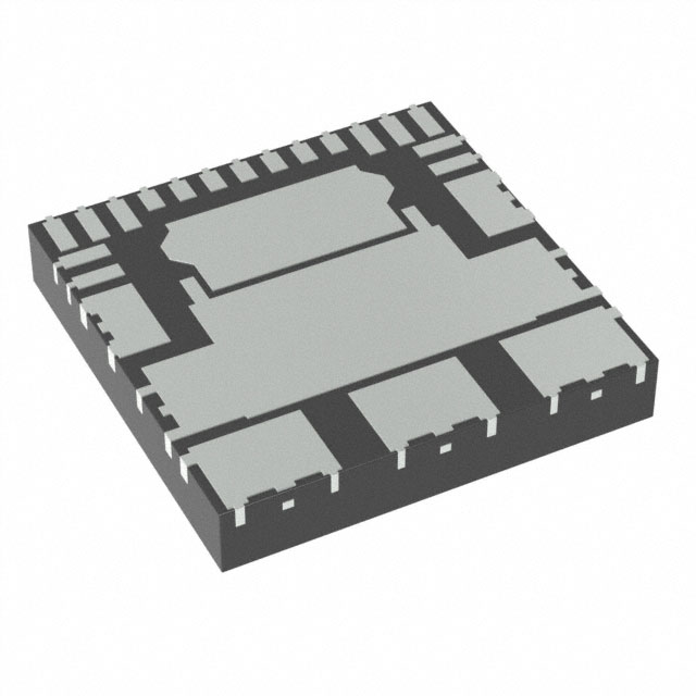
The 35XS3500 is packaged in a power-enhanced 12 x 12 mm
nonleaded PQFN package with exposed tabs.
Bottom View
Features
FK SUFFIX
98ART10511D
24-PIN PQFN
PB FREE
• Penta 35 m high side switches
• 16-bit SPI communication interface with daisy chain capability
• Current sense output with SPI-programmable multiplex switch
and board temperature feedback
• Digital diagnosis feature
• PWM module with multiphase feature including prescaler
• LEDs control including accurate current sensing and low dutycycle capability
• Fully protected switches
• Over-current shutdown detection
• Power net and reverse polarity protection
• Low-power mode
• Fail-safe mode functions including autorestart feature
• External smart power switch control including current recopy
12V
ORDERING INFORMATION
Device
(For Tape and Reel,
Add R2 Suffix)
MC35XS3500HFK
* MC35XS3500DHFK
12V
35XS3500
Watchdog
MCU
LIMP
FLASHER
STOP
IGN
RST
CLOCK
CS
VBAT
CP
OUT1
OUT2
OUT3
OUT4
OUT5
S0
FETIN
SI
SCLK
FETOUT
CSNS GND
Smart
Switch
Figure 1. 35XS3500 Simplified Application Diagram
Freescale Semiconductor, Inc. reserves the right to change the detail specifications,
as may be required, to permit improvements in the design of its products.
© Freescale Semiconductor, Inc., 2010-2013. All rights reserved.
Package
-40 to 125 °C
24 PQFN
* Recommended for all new designs
5.0V
VCC
Temperature
Range (TA)
�DEVICE VARIATIONS
DEVICE VARIATIONS
Table 1. MC35XS3500 Device Variations
Part Number
MC35XS3500HFK
MC35XS3500DHFK
Package
Temp.
24 PQFN
-40 to 125 °C
Comment
Initial release
D version is more robust against VBAT interrupt
35XS3500
2
Analog Integrated Circuit Device Data
Freescale Semiconductor
�INTERNAL BLOCK DIAGRAM
INTERNAL BLOCK DIAGRAM
VCC
VBAT
VCC failure
detection
RUP
Internal
Regulator
CP
OV/UV/POR
detections
Charge
Pump
CS
SO
SI
SCLK
Gate Drive
drain/gate clamp
Logic
LED Control
RDWN
OUT1
Over-current
Detection
CLOCK
LIMP
STOP
Open Load
Detection
FLASHER
IGN
RST
Over-temperature
Detection
OUT1
OUT2
OUT2
RDWN
OUT3
OUT3
Over-temperature
Prewarning
OUT4
OUT4
OUT5
OUT5
Selectable Output Current
Recopy (Analog MUX)
CSNS
Temperature
Feedback
FETIN
Current Recopy
Synchronization
VCC
Driver for External
MOSFET
FETOUT
GND
Figure 2. 35XS3500 Simplified Internal Block Diagram
35XS3500
Analog Integrated Circuit Device Data
Freescale Semiconductor
3
�PIN CONNECTIONS
SCLK
CS
STOP
LIMP
CLOCK
FLASHER
RST
IGN
FETIN
8
7
6
5
4
3
2
1
CP
16
GND
17
OUT5
18
VCC
9
SO
13 12 11 10
FETOUT
SI
PIN CONNECTIONS
14
GND
24
CSNS
23
GND
22
OUT1
15
VBAT
19
20
21
OUT4
OUT3
OUT2
Figure 3. 35XS3500 Pin Connections (Transparent Package Top View)
Table 2. 35XS3500 Pin Definitions
Functional descriptions these pins can be found in the Functional Description section beginning on page 20.
Pin
Pin Name
Pin Function
Formal Name
Definition
1
FETIN
Input
External FET Input
2
IGN
Input
Ignition Input
(Active High)
3
RST
Input
Reset
This input wakes the device. It is also used to initialize the device
configuration and fault registers through the SPI. This pin has a passive
internal pull-down.
4
FLASHER
Input
Flasher Input
(Active High)
This input wakes the device. This pin has a passive internal pull-down.
5
CLOCK
Input
Clock Input
This pin state depends on RST logic level.
As long as RST input pin is set to logic [0], this pin is pulled up in order to
report wake event. Otherwise, the PWM frequency and timing are
generated from this digital clock input by the PWM module.
This pin has a passive internal pull-down.
6
LIMP
Input
Limp Home Input
(Active High)
The Fail mode can be activated by this digital input. This pin has an active
internal pull-down current source.
7
STOP
Input
Stop Light Input
(Active High)
8
CS
Input
Chip Select
(Active Low)
9
SCLK
Input
SPI Clock Input
This pin is the current sense recopy of the external MOSFET.
This input wakes the device. It also controls outputs 1 and 2 in case of
Fail mode activation. This pin has a passive internal pull-down.
This input wakes the device. This pin has a passive internal pull-down.
When this signal is high, SPI signals are ignored. Asserting this pin low
starts a SPI transaction. The transaction is signaled as completed when
this signal returns high. This pin has a passive internal pull-up resistance.
This input pin is connected to the master microcontroller providing the
required bit shift clock for SPI communication. This pin has a passive
internal pull-down resistance.
35XS3500
4
Analog Integrated Circuit Device Data
Freescale Semiconductor
�PIN CONNECTIONS
Table 2. 35XS3500 Pin Definitions (continued)
Functional descriptions these pins can be found in the Functional Description section beginning on page 20.
Pin
Pin Name
Pin Function
Formal Name
Definition
10
SI
Input
Master-Out Slave-In
This data input is sampled on the positive edge of the SCLK. This pin has
a passive internal pull-down resistance.
11
VCC
Input
Logic Supply
12
SO
Output
Master-In Slave-Out
SPI data sent to the MCU by this pin. This data output changes on the
negative edge of SCLK, and when CS is high. This pin is high-impedance.
13
FETOUT
Output
External FET Gate
This pin controls an external SMART MOSFET by logic level. This output
called OUT6.
If OUT6 is not used in the application, this output pin is set to logic high
when the current sense output becomes valid when CSNS sync SPI bit is
set to logic [1].
14, 17, 23
GND
Ground
Ground
This pin is the ground for the logic and analog circuitry of the device.(1)
15
VBAT
Input
Battery Input
Power supply pin.
16
CP
Output
Charge Pump
This pin is the connection for an external tank capacitor (for internal use
only).
18
19
20
21
22
OUT5
OUT4
OUT3
OUT2
OUT1
Output
Output
Output
Output
Output
Output 5
Output 4
Output 3
Output 2
Output 1
24
CSNS
Output
Current Sense Output
SPI Logic power supply.
Protected 35 m high side power output to the load.
This pin is used to output a current proportional to OUT1:OUT5, FET in
current, and it is used externally to generate a ground-referenced voltage
for the microcontroller to monitor output current. Moreover, this pin can
report a voltage proportional to the temperature on the GND flag.
OUT1:OUT5, FET in current sensing and Temperature feedback choice is
SPI programmable.
Notes
1. The pins 14, 17, and 23 must be shorted on the board.
35XS3500
Analog Integrated Circuit Device Data
Freescale Semiconductor
5
�ELECTRICAL CHARACTERISTICS
MAXIMUM RATINGS
ELECTRICAL CHARACTERISTICS
MAXIMUM RATINGS
Table 3. Maximum Ratings
All voltages are with respect to ground unless otherwise noted. Exceeding these ratings may cause a malfunction or
permanent damage to the device.
Rating
Symbol
Value
Unit
ELECTRICAL RATINGS
Over-voltage Test Range
Maximum Operation Voltage
Load Dump (400 ms) at 25 °C
VBAT
Reverse Polarity Voltage Range
2.0 Min at 25 °C
VBAT
VCC Supply Voltage
VCC
Output Voltage
Positive
Negative (ground disconnected)
VOUT
Digital Input Current in Clamping Mode (SI, SCLK, CS, IGN, FLASHER,
STOP, LIMP)
FETIN Input Current
SO and FETOUT Output Voltage
Outputs clamp energy using single pulse method (L = 2.0 mH; R = 0 ;
VBAT = 14 V at 150 °C initial)
ESD Voltage(2)
Human Body Model (HBM) OUT[1:5], VPWR, and GND
Charge Device Model (CDM)
Corner Pins (1,13,19,21)
All Other Pins (2-12, 14-18, 20, 22-24)
V
28
40
V
- 18
-0.3 to 5.5
V
V
40
-16
IIN
±1.0
mA
IFETIN
+10
-1.0
mA
VSO
- 0.3 to VCC + 0.3
V
E
30
mJ
VESD
V
± 2000
± 8000
± 750
± 500
THERMAL RATINGS
Operating Temperature
Ambient
Junction
°C
TA
TJ
- 40 to 125
- 40 to 150
Peak Package Reflow Temperature During Reflow(3), (4)
TPPRT
Note 4
°C
Storage Temperature
TSTG
- 55 to 150
°C
RJC
1.0
C/W
THERMAL RESISTANCE
Thermal Resistance, Junction to Case(5)
Notes
2. ESD testing is performed in accordance with the Human Body Model (HBM) (CZAP = 100 pF, RZAP = 1500 ) and the Charge Device
Model.
3. Pin soldering temperature limit is for 40 seconds maximum duration. Not designed for immersion soldering. Exceeding these limits may
cause malfunction or permanent damage to the device.
4. Freescale’s Package Reflow capability meets Pb-free requirements for JEDEC standard J-STD-020C. For Peak Package Reflow
Temperature and Moisture Sensitivity Levels (MSL), Go to www.freescale.com, search by part number [e.g. remove prefixes/suffixes
and enter the core ID to view all orderable parts. (i.e. MC33xxxD enter 33xxx), and review parametrics.
5. Typical value is guaranteed per design.
35XS3500
6
Analog Integrated Circuit Device Data
Freescale Semiconductor
�ELECTRICAL CHARACTERISTICS
STATIC ELECTRICAL CHARACTERISTICS
STATIC ELECTRICAL CHARACTERISTICS
Table 4. Static Electrical Characteristics
Characteristics noted under conditions 3.0 V VCC 5.5 V, 7.0 V VBAT 20 V, -40C TA 125C, unless otherwise noted.
Typical values noted reflect the approximate parameter mean at TA = 25C under nominal conditions, unless otherwise noted.
Characteristic
Symbol
Min
Typ
Max
Unit
7.0
–
20
6.0
–
28
VBATUV
5.0
5.5
6.0
V
VBATCLAMP_OV
27.5
30
32.5
V
VBATCLAMP
40
–
48
V
Battery Supply Power on Reset(9)
If VBAT < 5.5 V, VBAT = VCC
VBATPOR1
2.0
–
3.0
If VBAT < 5.5 V, VBAT = 0
VBATPOR2
2.0
–
4.0
IBATSLEEP1
IBATSLEEP2
IBAT
–
–
–
0.5
0.5
10
5.0
5.0
20
A
A
mA
VCC
3.0
–
5.5
V
VCCUV
2.2
2.5
2.8
V
POWER INPUT (VBAT, VCC)
Battery Supply Voltage Range
Full Performance and Short-circuit
VBAT
Extended Voltage Range(6)
Battery Supply Under-voltage (UV flag is set ON)
Battery Voltage Clamp (OV flag is set ON)
Battery Voltage Clamp
V
V
VBAT Supply Current at 25 °C and VBAT =12 V and VCC = 5.0 V
Sleep State Current, Outputs Open
Sleep State Current, Outputs Grounded
Normal Mode, IGN = 5.0 V, RST = 5.0 V, Outputs Open
Digital Voltage Range, Full Performance
Digital Supply Under-voltage (VCC Failure)
Sleep Current Consumption on VCC at 25 °C and VBAT = 12 V
Output OFF
Supply Current Consumption on VCC and VBAT = 12 V
A
ICCSLEEP
–
0.2
5.0
–
–
2.6
–
–
5.0
ICC
No SPI
3.0 MHz SPI Communication
mA
LOGIC INPUT/ OUTPUT (IGN, CS, CSNS, SI, SCLK, CLOCK, SO, FLASHER, RST, LIMP, STOP)
Input High Logic Level(7)
VIH
2.0
–
–
V
Input Low Logic Level(7)
VIL
–
–
0.8
V
VIGNTH
1.0
2.2
V
Ignition Threshold Level (IGN, FLASHER, STOP and RST)
Input Clamp Voltage (IGN, FLASHER, LIMP, STOP, CS, SCLK, SI, RST)
I = 1.0 mA
VCL_POS
Input Forward Voltage (IGN, FLASHER, LIMP, STOP, CS, SCLK, SI, RST)
I = 1.0 mA
VCL_NEG
7.5
–
13
V
- 2.0
–
-0.3
V
RUP
100
200
400
k
Input Passive Pull-down Resistance on SI, SCLK, FLASHER, IGN, FOG,
CLOCK, LIMP and RST pins(8)
RDWN
100
200
500
k
SO High-state Output Voltage
IOH = 1.0 mA
VSOH
0.8
0.95
–
0.8
0.95
–
Input Passive Pull-up Resistance on CS pin(8)
CLOCK Output Voltage reporting wake-up event (ICLOCK=1.0 mA)
Notes
6.
7.
8.
9.
VCLOCKH
VCC
VCC
In extended mode, the functionality is guaranteed but not the electrical parameters.
Valid for RST, SI, SCLK, CLOCK, FLASHER, STOP, and LIMP pins.
Valid for the following input voltage range: VCC = -0.3 to +0.3 V.
Please refer to Loss of VBAT section for more details.
35XS3500
Analog Integrated Circuit Device Data
Freescale Semiconductor
7
�ELECTRICAL CHARACTERISTICS
STATIC ELECTRICAL CHARACTERISTICS
Table 4. Static Electrical Characteristics (continued)
Characteristics noted under conditions 3.0 V VCC 5.5 V, 7.0 V VBAT 20 V, -40C TA 125C, unless otherwise noted.
Typical values noted reflect the approximate parameter mean at TA = 25C under nominal conditions, unless otherwise noted.
Characteristic
Symbol
Min
Typ
Max
Unit
LOGIC INPUT/ OUTPUT (IGN, CS, CSNS, SI, SCLK, CLOCK, SO, FLASHER, RST, LIMP, STOP) (CONTINUED)
SO Low-state Output Voltage
IOL = -1.6 mA
VSOL
SO Tri-state Leakage Current
CS > 0.7 VCC
ISOLEAK
CSNS Tri-state Leakage Current
VCC = 5.5 V, CSNS = 4.5 V
VCC = 5.0 V, CSNS = 5.5 V
VCC = 5.0 V, CSNS = 3.0 V
Current Sense Output Clamp Voltage
ICSNS < 10.0 mA
V
–
0.2
0.4
- 1.0
0.0
1.0
- 5.0
- 10
- 1.0
0.0
0.0
0.0
1.0
1.0
1.0
5.0
6.0
7.0
–
–
0
20
2.0
25
- 22
–
-16
A
A
ICSNSLEAK
VCSNS
V
OUTPUT (OUT 1:5)
Output Leakage Current in OFF state
Sleep mode, Outputs Grounded
Normal mode, Outputs Grounded
Output Negative Clamp Voltage
IOUT = -500 mA, Outputs OFF
Current Sense Output Precision(10)
Full-Scale Range (FSR) for LED Control bit = 0
0.75 FSR
0.50 FSR
0.25 FSR
0.10 FSR
Full-Scale Range (FSR) for LED Control bit = 1
0.187 FSR = 0.75 FSRLED
0.125 FSR = 0.50 FSRLED
0.062 FSR = 0.25 FSRLED
0.025 FSR = 0.10 FSRLED
A
IOUTLEAK
VOUT
V
ICS / ICS
%
-14
-15
-17
-22
-
14
15
17
22
-13
-13
-20
-30
-
13
13
20
30
-6.0
-
6.0
-6.0
–
6.0
%
–
± 280
± 400
ppm/
°C
%
Current Sense Output Precision
Over-temperature Range [-40;125 °C], VBAT Range [10 V-16 V] and FSR
Range [25%-100%], calculated with one calibration point (Taken at 25 °C,
VBAT = 13.5 V and 50% FSR)(12)
Current Sense Output Precision with one calibration point (50% FSRLED,
VBAT = 13.5 at 25 °C(12)
Temperature Drift of Current Sense Output(11)
VBAT = 13.5 V, IOUT = 2.8 A reference taken at TA = 25 °C
ICS / T
Notes
10. 10 V < VBAT < 16 V. (ICS / ICS = (measured ICS- targeted ICS)/ targeted ICS with targeted ICS = 5.0 mA
11.
Based on statistical data. Not production tested. ICS / T = [(measured at ICS at T1 - measured at ICS at T2) measured at ICS at room]/
(T1 - T2)
12.
Based on statistical analysis covering 99.74% of parts.
35XS3500
8
Analog Integrated Circuit Device Data
Freescale Semiconductor
�ELECTRICAL CHARACTERISTICS
STATIC ELECTRICAL CHARACTERISTICS
Table 4. Static Electrical Characteristics (continued)
Characteristics noted under conditions 3.0 V VCC 5.5 V, 7.0 V VBAT 20 V, -40C TA 125C, unless otherwise noted.
Typical values noted reflect the approximate parameter mean at TA = 25C under nominal conditions, unless otherwise noted.
Characteristic
Symbol
Min
Typ
Max
Unit
65
–
–
40
–
–
TOTS
155
175
195
°C
TOTSWARN
110
125
140
°C
VOUT_TH
0.475
0.5
0.525
VBAT
OUTPUT (OUT 1:5) (CONTINUED)
Minimum Output Current Reported in CSNS for OUT[1-5](13)
10 V VBAT 16 V
Minimum Output Current Reported in CSNS for OUT[1-5] in LED Mode(13)
10 V VBAT 16 V
Over-temperature Shutdown
Thermal Prewarning(14)
Output Voltage Threshold
I35MIN(CSNS)
mA
I35MIN(CSNS) LED
mA
TAIL LIGHT (OUT1)
Output Drain-to-Source ON Resistance (IOUT = 2.8 A, TA = 25 °C)
RDS(ON)
m
VBAT = 13.5 V
–
–
35
VBAT = 7.0 V
–
–
55
Output Drain-to-Source ON Resistance (IOUT = 2.8 A, VBAT = 13.5 V,
TA = 150
RDS(ON)
°C)(14)
Reverse Output ON Resistance (IOUT = -2.8 A, VBAT = -12 V, TA = 25 °C)(15)
RSD(ON)
m
–
–
59.5
–
–
70
–
–
–
–
70
110
–
–
119
28.0
30.2
35.0
36.0
43.5
41.8
29.4
35.0
40.6
m
TAIL LIGHT (OUT1)
Output Drain-to-Source ON Resistance (IOUT = 1.5 A, TA = 25 °C) for LED
Control = 1
VBAT = 13.5 V
RDS(ON)25_LED
m
VBAT = 7.0 V
Output Drain-to-Source ON Resistance (IOUT = 1.5 A, VBAT = 13.5 V,
RDS(ON)150_LED
TA = 150 °C) for LED Control = 1
m
High Over-current Shutdown Threshold 1
VBAT = 16 V, TA = -40 °C
VBAT = 16 V, TA = 25 °C
VBAT = 16 V, TA = 125 °C
IOCHI1
28.3
33.8
39.3
High Over-current Shutdown Threshold 2
IOCHI2
12.3
15.4
18.5
A
Low Over-current Shutdown Threshold
IOCLO
5.7
7.2
8.9
A
IOL
0.05
0.2
0.5
A
Open Load Current Threshold in ON State(16)
Open Load Current Threshold in ON State with LED(17)
VOL = VBAT - 0.5 V
IOLLED
Current Sense Full-scale Range(18)
ICS FSR
A
mA
4.0
10
20
–
6.0
–
A
Notes
13. Output current value computed after leakage current removal (open load condition)
14. Parameter guaranteed by design; however it is not production tested.
15. Source-to-Drain ON Resistance (Reverse Drain-to-Source ON Resistance) with negative polarity VBAT.
16.
17.
18.
OLLED1, bit D0 in SI data is set to [0]
OLLED1, bit D0 in SI data is set to [1]
For a typical value of ICS FSR, ICSNS = 5.0 mA. If the range is exceeded, no current clamp and the precision is not guaranteed.
35XS3500
Analog Integrated Circuit Device Data
Freescale Semiconductor
9
�ELECTRICAL CHARACTERISTICS
STATIC ELECTRICAL CHARACTERISTICS
Table 4. Static Electrical Characteristics (continued)
Characteristics noted under conditions 3.0 V VCC 5.5 V, 7.0 V VBAT 20 V, -40C TA 125C, unless otherwise noted.
Typical values noted reflect the approximate parameter mean at TA = 25C under nominal conditions, unless otherwise noted.
Characteristic
Symbol
Min
Typ
Max
Unit
Current Sense Full-scale Range (19) depending on LED Control = 1
ICS FSR_LED
–
1.6
–
A
Severe Short-circuit Impedance Range (19)
RSC1(OUT1)
350
–
–
m
TAIL LIGHT (OUT1) (CONTINUED)
LICENSE LIGHT (OUT2)
Output Drain-to-Source ON Resistance (IOUT = 2.8 A, TA = 25 °C)
RDS(ON)
m
VBAT = 13.5 V
–
–
35
VBAT = 7.0 V
–
–
55
Output Drain-to-Source ON Resistance (IOUT = -2.8 A, VBAT = -13.5 V,
RDS(ON)
(20)
TA = 25 °C)
Reverse Output ON Resistance (IOUT = 2.8 A, VBAT = 12 V, TA = 150 °C)(21)
Output Drain-to-Source ON Resistance (IOUT =1.5 A, TA = 25 °C) for LED
Control = 1
VBAT = 13.5 V
RSD(ON)
m
–
–
59.5
–
–
70
–
–
–
–
70
110
–
–
119
28.0
30.2
35.0
36.0
43.5
41.8
29.4
35.0
40.6
28.3
33.8
39.3
RDS(ON)25_LED
m
m
VBAT = 7.0 V
Output Drain-to-Source ON Resistance (IOUT = 1.5 A, VBAT = 13.5 V,
RDS(ON)150_LED
TA = 150 °C) for LED Control = 1
m
High Over-current Shutdown Threshold 1
VBAT = 16 V, TA = -40 °C
VBAT = 16 V, TA = 25 °C
VBAT = 16 V, TA = 125 °C
IOCHI1
High Over-current Shutdown Threshold 2
IOCHI2
12.3
15.4
18.5
A
Low Over-current Shutdown Threshold
IOCLO
5.7
7.2
8.9
A
IOL
0.05
0.2
0.5
A
4.0
10
20
Open Load Current Threshold in ON State(22)
A
Open Load Current Threshold in ON State with LED(23)
VOL = VBAT - 0.5 V
IOLLED
mA
Current Sense Full-Scale Range(24)
ICS FSR
–
6.0
–
A
Current Sense Full-Scale Range(20) depending on LED Control = 1
ICS FSR_LED
–
1.6
–
A
Severe short-circuit impedance range(20)
RSC1(OUT2)
350
–
–
m
Notes
19. Output current value computed after leakage current removal (open load condition)
20. Parameter guaranteed by design; however, it is not production tested.
21. Source-to-Drain ON Resistance (Reverse Drain-to-Source ON Resistance) with negative polarity VBAT.
22.
23.
24.
OLLED2, bit D0 in SI data is set to [0]
OLLED2, bit D0 in SI data is set to [1]
For typical value of ICS FSR, ICSNS = 5.0 mA. If the range is exceeded, no current clamp and the precision is not guaranteed.
35XS3500
10
Analog Integrated Circuit Device Data
Freescale Semiconductor
�ELECTRICAL CHARACTERISTICS
STATIC ELECTRICAL CHARACTERISTICS
Table 4. Static Electrical Characteristics (continued)
Characteristics noted under conditions 3.0 V VCC 5.5 V, 7.0 V VBAT 20 V, -40C TA 125C, unless otherwise noted.
Typical values noted reflect the approximate parameter mean at TA = 25C under nominal conditions, unless otherwise noted.
Characteristic
Symbol
Min
Typ
Max
VBAT = 13.5 V
–
–
35
VBAT = 7.0 V
–
–
55
–
–
59.5
–
–
70
–
–
–
–
70
110
–
–
119
28.0
30.2
35.0
36.0
43.5
41.8
29.4
35.0
40.6
28.3
33.8
39.3
Unit
TAIL LIGHT (OUT3)
Output Drain-to-Source ON Resistance (IOUT = 2.8 A, TA = 25 °C)
Output Drain-to-Source ON Resistance (IOUT = 2.8 A, VBAT = 13.5 V,
RDS(ON)25
RDS(ON)150
TA = 150 °C)(25)
Reverse Source-to-Drain ON Resistance (IOUT = -2.8 A, VBAT = -12 V,
m
RSD(ON)25
m
m
TA = 25 °C)(26)
Output Drain-to-Source ON Resistance (IOUT = 1.5 A, TA = 25 °C) for LED
Control = 1
VBAT = 13.5 V
RDS(ON)25_LED
m
VBAT = 7.0 V
Output Drain-to-Source ON Resistance (IOUT = 1.5 A, VBAT = 13.5 V,
RDS(ON)150_LED
TA = 150 °C) for LED Control = 1
m
High Over Current Shutdown Threshold 1
VBAT = 16 V, TA = -40 °C
VBAT = 16 V, TA = 25 °C
VBAT = 16 V, TA = 125 °C
IOCHI1
High Over-current Shutdown Threshold 2
IOCHI2
12.3
15.4
18.5
A
Low Over-current Shutdown Threshold
IOCLO
5.7
7.2
8.9
A
IOL
0.05
0.2
0.5
A
4.0
10
20
Open Load Current Threshold in ON State(27)
A
Open Load Current Threshold in ON State with LED(28)
VOL = VBAT - 0.5 V
IOLLED
mA
Current Sense Full-scale Range(29)
ICS FSR
–
6.0
–
A
Current Sense Full-scale Range(25) depending on LED Control = 1
ICS FSR_LED
–
1.6
–
A
Severe short-circuit impedance range(25)
RSC1(OUT3)
350
–
–
m
Notes
25. Parameter guaranteed by design; however, it is not production tested.
26. Source-to-Drain ON Resistance (Reverse Drain-to-Source ON Resistance) with negative polarity VBAT.
27.
28.
29.
OLLED3, bit D2 in SI data is set to [0]
OLLED3, bit D2 in SI data is set to [1]
For a typical value of ICS FSR, ICSNS = 5.0 mA. If the range is exceeded, no current clamp and the precision is not guaranteed.
35XS3500
Analog Integrated Circuit Device Data
Freescale Semiconductor
11
�ELECTRICAL CHARACTERISTICS
STATIC ELECTRICAL CHARACTERISTICS
Table 4. Static Electrical Characteristics (continued)
Characteristics noted under conditions 3.0 V VCC 5.5 V, 7.0 V VBAT 20 V, -40C TA 125C, unless otherwise noted.
Typical values noted reflect the approximate parameter mean at TA = 25C under nominal conditions, unless otherwise noted.
Characteristic
Symbol
Min
Typ
Max
VBAT = 13.5 V
–
–
35
VBAT = 7.0 V
–
–
55
–
–
59.5
Unit
STOP LIGHT (OUT4)
Output Drain-to-Source ON Resistance (IOUT = 2.8 A, TA = 25 °C)
Output Drain-to-Source ON Resistance (IOUT = 2.8 A, VBAT = 13.5 V,
RDS(ON)25
RDS(ON)150
TA = 150 °C)(30)
Output Drain-to-Source ON Resistance (IOUT = 1.5 A, TA = 25 °C) for LED
Control = 1
VBAT = 13.5 V
m
m
RDS(ON)25_LED
m
–
–
–
–
70
110
–
–
119
RDS(ON)25
–
–
70
m
High Over-current Shutdown Threshold 1
VBAT = 16 V, TA = -40 °C
VBAT = 16 V, TA = 25 °C
VBAT = 16 V, TA = 125 °C
IOCHI1
28.0
30.2
35.0
36.0
43.5
41.8
A
29.4
35.0
40.6
28.3
33.8
39.3
High Over-current Shutdown Threshold 2
IOCHI2
12.3
15.4
18.5
A
Low Over-current Shutdown Threshold
IOCLO
5.7
7.2
8.9
A
IOL
0.05
0.2
0.5
A
4.0
10
20
VBAT = 7.0 V
Output Drain-to-Source ON Resistance (IOUT =1.5 A, VBAT = 13.5 V,
RDS(ON)150_LED
TA = 150 °C) for LED Control = 1
Reverse Source-to-Drain ON Resistance (IOUT = -2.8 A, VBAT = -12 V,
m
TA = 25 °C)(31)
Open Load Current Threshold in ON State(32)
Open Load Current Threshold in ON State with LED(33)
VOL = VBAT - 0.5 V
IOLLED
mA
Current Sense Full-scale Range(34)
ICS FSR
–
6.0
–
A
Current Sense Full-scale Range(30) depending on LED Control = 1
ICS FSR_LED
–
1.6
–
A
Severe Short-circuit Impedance Range(30)
RSC1(OUT4)
350
m
Notes
30. Parameter guaranteed by design; however, it is not production tested.
31. Source-to-Drain ON Resistance (Reverse Drain-to-Source ON Resistance) with negative polarity VBAT.
32.
33.
34.
OLLED3, bit D2 in SI data is set to [0]
OLLED3, bit D2 in SI data is set to [1]
For a typical value of ICS FSR, ICSNS = 5.0 mA. If the range is exceeded, no current clamp and the precision is not guaranteed.
35XS3500
12
Analog Integrated Circuit Device Data
Freescale Semiconductor
�ELECTRICAL CHARACTERISTICS
STATIC ELECTRICAL CHARACTERISTICS
Table 4. Static Electrical Characteristics (continued)
Characteristics noted under conditions 3.0 V VCC 5.5 V, 7.0 V VBAT 20 V, -40C TA 125C, unless otherwise noted.
Typical values noted reflect the approximate parameter mean at TA = 25C under nominal conditions, unless otherwise noted.
Characteristic
Symbol
Min
Typ
Max
VBAT = 13.5 V
–
–
35
VBAT = 7.0 V
–
–
55
–
–
59.5
–
–
70
Unit
FLASHER (OUT5)
Output Drain-to-Source ON Resistance (IOUT = 2.8 A, TA = 25 °C)
Output Drain-to-Source ON Resistance (IOUT = 2.8 A, VBAT = 13.5 V,
TA = 150
RDS(ON)25
RDS(ON)150
°C)(35)
Reverse Source-to-Drain ON Resistance (IOUT = -2.8 A, VBAT = -12 V,
m
RSD(ON)25
m
m
TA = 25 °C)(36)
Output Drain-to-Source ON Resistance (IOUT =1.5 A, TA = 25 °C) for LED
Control = 1
VBAT = 13.5 V
RDS(ON)25_LED
VBAT = 7.0 V
Output Drain-to-Source ON Resistance (IOUT = 1.5 A, VBAT = 13.5 V,
m
–
–
–
–
70
110
–
–
119
28.0
30.2
35.0
36.0
43.5
41.8
29.4
35.0
40.6
28.3
33.8
39.3
RDS(ON)150_LED
TA = 150 °C) for LED Control = 1
m
High Over-current Shutdown Threshold 1
VBAT = 16 V, TA = -40 °C
VBAT = 16 V, TA = 25 °C
VBAT = 16 V, TA = 125 °C
IOCHI1
High Over-current Shutdown Threshold 2
IOCHI2
12.3
15.4
18.5
A
Low Over-current Shutdown Threshold
IOCLO
5.7
7.2
8.9
A
IOL
0.05
0.2
0.5
A
4.0
10
20
Open Load Current Threshold in ON State(37)
A
Open Load Current Threshold in ON State with LED(38)
VOL = VBAT - 0.5 V
IOLLED
mA
Current Sense Full-scale Range(39)
ICS FSR
–
6.0
–
A
Current Sense Full-scale Range(35) depending on LED Control = 1
ICS FSR_LED
–
1.6
–
A
Severe Short-circuit Impedance Range(35)
RSC1(OUT5)
350
–
–
m
Notes
35. Parameter guaranteed by design; however, it is not production tested.
36. Source-to-Drain ON Resistance (Reverse Drain-to-Source ON Resistance) with negative polarity VBAT.
37.
38.
39.
OLLED3, bit D2 in SI data is set to [0]
OLLED3, bit D2 in SI data is set to [1]
For a typical value of ICS FSR, ICSNS = 5.0 mA. If the range is exceeded, no current clamp and the precision is not guaranteed.
35XS3500
Analog Integrated Circuit Device Data
Freescale Semiconductor
13
�ELECTRICAL CHARACTERISTICS
STATIC ELECTRICAL CHARACTERISTICS
Table 4. Static Electrical Characteristics (continued)
Characteristics noted under conditions 3.0 V VCC 5.5 V, 7.0 V VBAT 20 V, -40C TA 125C, unless otherwise noted.
Typical values noted reflect the approximate parameter mean at TA = 25C under nominal conditions, unless otherwise noted.
Characteristic
Symbol
Min
Typ
Max
Unit
FETOUT Output High Level at I = 1.0 mA
VH MAX
0.8
–
–
VCC
FETOUT Output Low Level at I = 1.0 mA
VH MIN
–
0.2
0.4
V
FETIN Input Full Scale Range Current
IFET IN
–
5.0
–
mA
FETIN Input Clamp Voltage
VCLIN
5.3
–
7.0
V
Drop Voltage between FETIN and CSNS for MUX[2:0] = 110
IFET IN = 5 mA, 5.5 V > CSNS > 0.0 V
VDRIN
0.0
–
0.4
- 1.0
- 1.0
–
–
5.0
1.0
VT_FEED
920
1025
1140
mV
Analog Temperature Feedback Derating with 5.0 k > RCSNS > 500 (40)
VDT_FEED
10.9
11.3
11.7
mV/ °C
Analog Temperature Feedback Precision(40)
VDT_ACC
-15
–
15
°C
VDT_ACC_CAL
-5.0
–
5.0
°C
SPARE (FETOUT , FETIN)
FETIN Leakage Current when external current switch sense is enabled
4.5 V > VFET IN > 0 V, 5.5 V > VCC > 4.5 V, CSNS open
V
A
IFETINLEAK
3.0 V > VFET IN > 0 V, 4.5 V > VCC > 0, CSNS open
TEMPERATURE OF GND FLAG
Analog Temperature Feedback at TA = 25 °C with 5.0 k > RCSNS > 500
Analog Temperature Feedback Precision with calibration point at 25 °C(40)
Notes
40. Parameter guaranteed by design; however, it is not production tested.
35XS3500
14
Analog Integrated Circuit Device Data
Freescale Semiconductor
�ELECTRICAL CHARACTERISTICS
DYNAMIC ELECTRICAL CHARACTERISTICS
DYNAMIC ELECTRICAL CHARACTERISTICS
Table 5. Dynamic Electrical Characteristics
Characteristics noted under conditions 4.5 V VCC 5.5 V, 7.0 V VBAT 20 V, -40C TA 125C, unless otherwise noted.
Typical values noted reflect the approximate parameter mean at TA = 25C under nominal conditions, unless otherwise noted.
Characteristic
Symbol
Min
Typ
Max
Unit
POWER OUTPUTS TIMING (OUT1:5)
Current Sense Valid Time on resistive load only(41)
SR bit = 0
SR bit = 1
t CSNS(VAL)
Current Sense Synchronization Time on FETOUT
SR bit = 0
SR bit = 1
t CSNS(SYNC)
s
–
90
150
–
45
75
–
130
185
–
70
110
–
10
30
SR bit = 0, IOUT = 2.8 A
0.10
0.25
0.56
SR bit = 1, IOUT = 0.7 A
0.20
0.40
0.80
0.10
0.25
0.56
0.20
0.40
0.80
0.8
1.0
1.2
Current Sense Settling Time on resistive load only
(41)
Driver Output Positive Slew Rate (30% to 70% at VBAT = 14 V)
Driver Output Negative Slew Rate (70% to 30% at VBAT = 14 V)
SR bit = 0, IOUT = 2.8 A
t CSNS(SET)
SRR
SRF
SR bit = 1, IOUT = 0.7 A
Driver Output Matching Slew Rate (SRR/SRF)(70% to 30% at VBAT = 14 V
at 25 °C)
Driver Output Turn-ON Delay (SPI ON Command [No PWM, CS Positive
Edge] to Output = 50% VBAT at VBAT = 14 V)
s
V/s
V/s
SR
s
t DLYON
SR bit = 0, IOUT = 2.8 A
50
–
120
SR bit = 1, IOUT = 0.7 A
25
–
65
Driver Output Turn-OFF Delay (SPI OFF command [CS Positive Edge] to
Output = 50% VBAT at VBAT = 14 V)
s
t DLYOFF
SR bit = 0, IOUT = 2.8 A
50
–
120
SR bit = 1, IOUT = 0.7 A
25
–
65
Driver Output Matching Time (t DLY(ON) - t DLY(OFF)) at Output = 50% VBAT
with VBAT = 14 V, f PWM = 240 Hz, PWM = 50%, at 25 °C
SR bit = 0, IOUT = 2.8 A for OUT1/2/3/4/5
SR bit = 1, IOUT = 0.7 A for OUT1/2/3/4/5
s
s
t RF
-40
-23
–
20
–
7.0
Notes
41. Not production tested.
35XS3500
Analog Integrated Circuit Device Data
Freescale Semiconductor
15
�ELECTRICAL CHARACTERISTICS
DYNAMIC ELECTRICAL CHARACTERISTICS
Table 5. Dynamic Electrical Characteristics (continued)
Characteristics noted under conditions 4.5 V VCC 5.5 V, 7.0 V VBAT 20 V, -40C TA 125C, unless otherwise noted.
Typical values noted reflect the approximate parameter mean at TA = 25C under nominal conditions, unless otherwise noted.
Characteristic
Symbol
Min
Typ
Max
Unit
Nominal PWM Frequency Range(44)
f PWM
30
–
400
Hz
Clock Input Frequency Range
f CLK
7.68
–
51.2
kHz
PWM_MAX
4.0
–
96
%
Output PWM Duty Cycle linear range for 11 V