MC68HC705C9A
Advance Information Data Sheet
M68HC05
Microcontrollers
MC68HC705C9A
Rev. 4.1
9/2005
freescale.com
This document contains certain information on a new product.Specifications and information herein are subject to change without notice.
�Blank
�MC68HC705C9A
Advance Information Data Sheet
To provide the most up-to-date information, the revision of our documents on the World Wide Web will be
the most current. Your printed copy may be an earlier revision. To verify you have the latest information
available, refer to:
http://www.freescale.com/
The following revision history table summarizes changes contained in this document. For your
convenience, the page number designators have been linked to the appropriate location.
Revision History
Date
Revision
Level
Description
Page
Number(s)
Format update to current publication standards
N/A
Figure 12-10. SPI Slave Timing Diagram — Corrected labels for
MISO and MOSI and subtitle for part b.
145
4.0
Figure 8-3. Timer Status Register (TSR) — Corrected
address designator from $0012 to $0013.
78
4.1
Updated to meet Freescale identity guidelines.
October,
2001
3.0
February,
2002
September,
2005
Throughout
MC68HC05C9A Advance Information Data Sheet, Rev. 4.1
Freescale Semiconductor
3
�Revision History
MC68HC05C9A Advance Information Data Sheet, Rev. 4.1
4
Freescale Semiconductor
�List of Chapters
Chapter 1 General Description. . . . . . . . . . . . . . . . . . . . . . . . . . . . . . . . . . . . . . . . . . . . . . . . 13
Chapter 2 Memory . . . . . . . . . . . . . . . . . . . . . . . . . . . . . . . . . . . . . . . . . . . . . . . . . . . . . . . . . . 25
Chapter 3 Central Processor Unit (CPU). . . . . . . . . . . . . . . . . . . . . . . . . . . . . . . . . . . . . . . . 33
Chapter 4 Interrupts . . . . . . . . . . . . . . . . . . . . . . . . . . . . . . . . . . . . . . . . . . . . . . . . . . . . . . . . 35
Chapter 5 Resets . . . . . . . . . . . . . . . . . . . . . . . . . . . . . . . . . . . . . . . . . . . . . . . . . . . . . . . . . . . 39
Chapter 6 Low-Power Modes . . . . . . . . . . . . . . . . . . . . . . . . . . . . . . . . . . . . . . . . . . . . . . . . .45
Chapter 7 Input/Output (I/O) Ports. . . . . . . . . . . . . . . . . . . . . . . . . . . . . . . . . . . . . . . . . . . . . 47
Chapter 8 Capture/Compare Timer . . . . . . . . . . . . . . . . . . . . . . . . . . . . . . . . . . . . . . . . . . . . 51
Chapter 9 Serial Communications Interface (SCI) . . . . . . . . . . . . . . . . . . . . . . . . . . . . . . . . 59
Chapter 10 Serial Peripheral Interface (SPI) . . . . . . . . . . . . . . . . . . . . . . . . . . . . . . . . . . . . . 71
Chapter 11 Instruction Set . . . . . . . . . . . . . . . . . . . . . . . . . . . . . . . . . . . . . . . . . . . . . . . . . . . 79
Chapter 12 Electrical Specifications . . . . . . . . . . . . . . . . . . . . . . . . . . . . . . . . . . . . . . . . . . . 93
Chapter 13 Mechanical Specifications . . . . . . . . . . . . . . . . . . . . . . . . . . . . . . . . . . . . . . . . 107
Chapter 14 Ordering Information. . . . . . . . . . . . . . . . . . . . . . . . . . . . . . . . . . . . . . . . . . . . . 111
Appendix A EPROM Programming . . . . . . . . . . . . . . . . . . . . . . . . . . . . . . . . . . . . . . . . . . . 113
Appendix B M68HC05Cx Family Feature Comparisons . . . . . . . . . . . . . . . . . . . . . . . . . . 115
MC68HC05C9A Advance Information Data Sheet, Rev. 4.1
Freescale Semiconductor
5
�List of Chapters
MC68HC05C9A Advance Information Data Sheet, Rev. 4.1
6
Freescale Semiconductor
�Table of Contents
Chapter 1
General Description
1.1
1.2
1.3
1.4
1.4.1
1.4.2
1.5
1.6
1.6.1
1.6.2
1.6.3
1.6.4
1.6.5
1.6.6
1.6.7
1.6.8
1.6.9
1.6.10
1.6.11
Introduction . . . . . . . . . . . . . . . . . . . . . . . . . . . . . . . . . . . . . . . . . . . . . . . . . . . . . . . . . . . . . . . .
Features. . . . . . . . . . . . . . . . . . . . . . . . . . . . . . . . . . . . . . . . . . . . . . . . . . . . . . . . . . . . . . . . . . .
Configuration Options . . . . . . . . . . . . . . . . . . . . . . . . . . . . . . . . . . . . . . . . . . . . . . . . . . . . . . . .
Mask Options . . . . . . . . . . . . . . . . . . . . . . . . . . . . . . . . . . . . . . . . . . . . . . . . . . . . . . . . . . . . . . .
Port B Mask Option Register (PBMOR) . . . . . . . . . . . . . . . . . . . . . . . . . . . . . . . . . . . . . . . .
C12 Mask Option Register (C12MOR). . . . . . . . . . . . . . . . . . . . . . . . . . . . . . . . . . . . . . . . .
Software-Programmable Options (MC68HC05C9A Mode Only) . . . . . . . . . . . . . . . . . . . . . . . .
Functional Pin Descriptions . . . . . . . . . . . . . . . . . . . . . . . . . . . . . . . . . . . . . . . . . . . . . . . . . . . .
VDD and VSS . . . . . . . . . . . . . . . . . . . . . . . . . . . . . . . . . . . . . . . . . . . . . . . . . . . . . . . . . . . .
VPP . . . . . . . . . . . . . . . . . . . . . . . . . . . . . . . . . . . . . . . . . . . . . . . . . . . . . . . . . . . . . . . . . . . .
IRQ. . . . . . . . . . . . . . . . . . . . . . . . . . . . . . . . . . . . . . . . . . . . . . . . . . . . . . . . . . . . . . . . . . . .
OSC1 andOSC2. . . . . . . . . . . . . . . . . . . . . . . . . . . . . . . . . . . . . . . . . . . . . . . . . . . . . . . . . .
RESET . . . . . . . . . . . . . . . . . . . . . . . . . . . . . . . . . . . . . . . . . . . . . . . . . . . . . . . . . . . . . . . . .
TCAP . . . . . . . . . . . . . . . . . . . . . . . . . . . . . . . . . . . . . . . . . . . . . . . . . . . . . . . . . . . . . . . . . .
TCMP . . . . . . . . . . . . . . . . . . . . . . . . . . . . . . . . . . . . . . . . . . . . . . . . . . . . . . . . . . . . . . . . . .
PA0–PA7 . . . . . . . . . . . . . . . . . . . . . . . . . . . . . . . . . . . . . . . . . . . . . . . . . . . . . . . . . . . . . . .
PB0–PB7 . . . . . . . . . . . . . . . . . . . . . . . . . . . . . . . . . . . . . . . . . . . . . . . . . . . . . . . . . . . . . . .
PC0–PC7 . . . . . . . . . . . . . . . . . . . . . . . . . . . . . . . . . . . . . . . . . . . . . . . . . . . . . . . . . . . . . . .
PD0–PD5 and PD7 . . . . . . . . . . . . . . . . . . . . . . . . . . . . . . . . . . . . . . . . . . . . . . . . . . . . . . .
13
13
15
16
16
16
18
19
22
22
22
22
23
23
23
23
23
23
23
Chapter 2
Memory
2.1
2.2
2.3
2.4
2.5
2.6
Introduction . . . . . . . . . . . . . . . . . . . . . . . . . . . . . . . . . . . . . . . . . . . . . . . . . . . . . . . . . . . . . . . .
RAM . . . . . . . . . . . . . . . . . . . . . . . . . . . . . . . . . . . . . . . . . . . . . . . . . . . . . . . . . . . . . . . . . . . . . .
EPROM . . . . . . . . . . . . . . . . . . . . . . . . . . . . . . . . . . . . . . . . . . . . . . . . . . . . . . . . . . . . . . . . . . .
EPROM Security . . . . . . . . . . . . . . . . . . . . . . . . . . . . . . . . . . . . . . . . . . . . . . . . . . . . . . . . . . . .
ROM. . . . . . . . . . . . . . . . . . . . . . . . . . . . . . . . . . . . . . . . . . . . . . . . . . . . . . . . . . . . . . . . . . . . . .
I/O Registers . . . . . . . . . . . . . . . . . . . . . . . . . . . . . . . . . . . . . . . . . . . . . . . . . . . . . . . . . . . . . . .
25
25
25
28
28
28
Chapter 3
Central Processor Unit (CPU)
3.1
3.2
3.2.1
3.2.2
3.2.3
3.2.4
3.2.5
Introduction . . . . . . . . . . . . . . . . . . . . . . . . . . . . . . . . . . . . . . . . . . . . . . . . . . . . . . . . . . . . . . . .
CPU Registers . . . . . . . . . . . . . . . . . . . . . . . . . . . . . . . . . . . . . . . . . . . . . . . . . . . . . . . . . . . . . .
Accumulator (A) . . . . . . . . . . . . . . . . . . . . . . . . . . . . . . . . . . . . . . . . . . . . . . . . . . . . . . . . . .
Index Register (X) . . . . . . . . . . . . . . . . . . . . . . . . . . . . . . . . . . . . . . . . . . . . . . . . . . . . . . . .
Program Counter (PC) . . . . . . . . . . . . . . . . . . . . . . . . . . . . . . . . . . . . . . . . . . . . . . . . . . . . .
Stack Pointer (SP) . . . . . . . . . . . . . . . . . . . . . . . . . . . . . . . . . . . . . . . . . . . . . . . . . . . . . . . .
Condition Code Register (CCR). . . . . . . . . . . . . . . . . . . . . . . . . . . . . . . . . . . . . . . . . . . . . .
33
33
34
34
34
34
34
MC68HC05C9A Advance Information Data Sheet, Rev. 4.1
Freescale Semiconductor
7
�Table of Contents
Chapter 4
Interrupts
4.1
4.2
4.3
4.4
4.5
4.6
Introduction . . . . . . . . . . . . . . . . . . . . . . . . . . . . . . . . . . . . . . . . . . . . . . . . . . . . . . . . . . . . . . . .
Non-Maskable Software Interrupt (SWI) . . . . . . . . . . . . . . . . . . . . . . . . . . . . . . . . . . . . . . . . . .
External Interrupt (IRQ or Port B) . . . . . . . . . . . . . . . . . . . . . . . . . . . . . . . . . . . . . . . . . . . . . . .
Timer Interrupt . . . . . . . . . . . . . . . . . . . . . . . . . . . . . . . . . . . . . . . . . . . . . . . . . . . . . . . . . . . . . .
SCI Interrupt. . . . . . . . . . . . . . . . . . . . . . . . . . . . . . . . . . . . . . . . . . . . . . . . . . . . . . . . . . . . . . . .
SPI Interrupt. . . . . . . . . . . . . . . . . . . . . . . . . . . . . . . . . . . . . . . . . . . . . . . . . . . . . . . . . . . . . . . .
35
35
36
38
38
38
Chapter 5
Resets
5.1
5.2
5.3
5.4
5.5
5.5.1
5.5.2
5.6
5.7
5.8
5.9
5.9.1
5.9.2
Introduction . . . . . . . . . . . . . . . . . . . . . . . . . . . . . . . . . . . . . . . . . . . . . . . . . . . . . . . . . . . . . . . .
Power-On Reset (POR) . . . . . . . . . . . . . . . . . . . . . . . . . . . . . . . . . . . . . . . . . . . . . . . . . . . . . . .
RESET Pin. . . . . . . . . . . . . . . . . . . . . . . . . . . . . . . . . . . . . . . . . . . . . . . . . . . . . . . . . . . . . . . . .
Computer Operating Properly (COP) Reset . . . . . . . . . . . . . . . . . . . . . . . . . . . . . . . . . . . . . . .
MC68HC05C9A Compatible COP . . . . . . . . . . . . . . . . . . . . . . . . . . . . . . . . . . . . . . . . . . . . . . .
C9A COP Reset Register. . . . . . . . . . . . . . . . . . . . . . . . . . . . . . . . . . . . . . . . . . . . . . . . . . .
C9A COP Control Register . . . . . . . . . . . . . . . . . . . . . . . . . . . . . . . . . . . . . . . . . . . . . . . . .
MC68HC05C12A Compatible COP . . . . . . . . . . . . . . . . . . . . . . . . . . . . . . . . . . . . . . . . . . . . . .
MC68HC05C12A Compatible COP Clear Register . . . . . . . . . . . . . . . . . . . . . . . . . . . . . . . . . .
COP During Wait Mode . . . . . . . . . . . . . . . . . . . . . . . . . . . . . . . . . . . . . . . . . . . . . . . . . . . . . . .
COP During Stop Mode . . . . . . . . . . . . . . . . . . . . . . . . . . . . . . . . . . . . . . . . . . . . . . . . . . . . . . .
Clock Monitor Reset. . . . . . . . . . . . . . . . . . . . . . . . . . . . . . . . . . . . . . . . . . . . . . . . . . . . . . .
STOP Instruction Disable Option . . . . . . . . . . . . . . . . . . . . . . . . . . . . . . . . . . . . . . . . . . . . .
39
39
39
40
41
41
41
42
43
43
43
43
44
Chapter 6
Low-Power Modes
6.1
6.2
6.3
Introduction . . . . . . . . . . . . . . . . . . . . . . . . . . . . . . . . . . . . . . . . . . . . . . . . . . . . . . . . . . . . . . . . 45
Stop Mode . . . . . . . . . . . . . . . . . . . . . . . . . . . . . . . . . . . . . . . . . . . . . . . . . . . . . . . . . . . . . . . . . 45
Wait Mode . . . . . . . . . . . . . . . . . . . . . . . . . . . . . . . . . . . . . . . . . . . . . . . . . . . . . . . . . . . . . . . . . 46
Chapter 7
Input/Output (I/O) Ports
7.1
7.2
7.3
7.4
7.5
Introduction . . . . . . . . . . . . . . . . . . . . . . . . . . . . . . . . . . . . . . . . . . . . . . . . . . . . . . . . . . . . . . . .
Port A . . . . . . . . . . . . . . . . . . . . . . . . . . . . . . . . . . . . . . . . . . . . . . . . . . . . . . . . . . . . . . . . . . . . .
Port B . . . . . . . . . . . . . . . . . . . . . . . . . . . . . . . . . . . . . . . . . . . . . . . . . . . . . . . . . . . . . . . . . . . . .
Port C. . . . . . . . . . . . . . . . . . . . . . . . . . . . . . . . . . . . . . . . . . . . . . . . . . . . . . . . . . . . . . . . . . . . .
Port D. . . . . . . . . . . . . . . . . . . . . . . . . . . . . . . . . . . . . . . . . . . . . . . . . . . . . . . . . . . . . . . . . . . . .
47
47
48
48
48
Chapter 8
Capture/Compare Timer
8.1
8.2
8.2.1
8.2.2
Introduction . . . . . . . . . . . . . . . . . . . . . . . . . . . . . . . . . . . . . . . . . . . . . . . . . . . . . . . . . . . . . . . .
Timer Operation . . . . . . . . . . . . . . . . . . . . . . . . . . . . . . . . . . . . . . . . . . . . . . . . . . . . . . . . . . . . .
Input Capture . . . . . . . . . . . . . . . . . . . . . . . . . . . . . . . . . . . . . . . . . . . . . . . . . . . . . . . . . . . .
Output Compare. . . . . . . . . . . . . . . . . . . . . . . . . . . . . . . . . . . . . . . . . . . . . . . . . . . . . . . . . .
51
52
52
52
MC68HC05C9A Advance Information Data Sheet, Rev. 4.1
8
Freescale Semiconductor
�Table of Contents
8.3
8.3.1
8.3.2
8.3.3
8.3.4
8.3.5
8.3.6
8.4
8.5
Timer I/O Registers . . . . . . . . . . . . . . . . . . . . . . . . . . . . . . . . . . . . . . . . . . . . . . . . . . . . . . . . . .
Timer Control Register . . . . . . . . . . . . . . . . . . . . . . . . . . . . . . . . . . . . . . . . . . . . . . . . . . . . .
Timer Status Register . . . . . . . . . . . . . . . . . . . . . . . . . . . . . . . . . . . . . . . . . . . . . . . . . . . . .
Timer Registers . . . . . . . . . . . . . . . . . . . . . . . . . . . . . . . . . . . . . . . . . . . . . . . . . . . . . . . . . .
Alternate Timer Registers . . . . . . . . . . . . . . . . . . . . . . . . . . . . . . . . . . . . . . . . . . . . . . . . . .
Input Capture Registers . . . . . . . . . . . . . . . . . . . . . . . . . . . . . . . . . . . . . . . . . . . . . . . . . . . .
Output Compare Registers . . . . . . . . . . . . . . . . . . . . . . . . . . . . . . . . . . . . . . . . . . . . . . . . .
Timer During Wait Mode . . . . . . . . . . . . . . . . . . . . . . . . . . . . . . . . . . . . . . . . . . . . . . . . . . . . . .
Timer During Stop Mode . . . . . . . . . . . . . . . . . . . . . . . . . . . . . . . . . . . . . . . . . . . . . . . . . . . . . .
52
53
54
55
55
56
56
57
57
Chapter 9
Serial Communications Interface (SCI)
9.1
9.2
9.3
9.4
9.5
9.6
9.7
9.8
9.9
9.10
9.11
9.12
9.13
9.13.1
9.13.2
9.13.3
9.13.4
9.13.5
Introduction . . . . . . . . . . . . . . . . . . . . . . . . . . . . . . . . . . . . . . . . . . . . . . . . . . . . . . . . . . . . . . . .
Features. . . . . . . . . . . . . . . . . . . . . . . . . . . . . . . . . . . . . . . . . . . . . . . . . . . . . . . . . . . . . . . . . . .
SCI Receiver Features. . . . . . . . . . . . . . . . . . . . . . . . . . . . . . . . . . . . . . . . . . . . . . . . . . . . . . . .
SCI Transmitter Features. . . . . . . . . . . . . . . . . . . . . . . . . . . . . . . . . . . . . . . . . . . . . . . . . . . . . .
Functional Description . . . . . . . . . . . . . . . . . . . . . . . . . . . . . . . . . . . . . . . . . . . . . . . . . . . . . . . .
Data Format . . . . . . . . . . . . . . . . . . . . . . . . . . . . . . . . . . . . . . . . . . . . . . . . . . . . . . . . . . . . . . . .
Receiver Wakeup Operation . . . . . . . . . . . . . . . . . . . . . . . . . . . . . . . . . . . . . . . . . . . . . . . . . . .
Idle Line Wakeup . . . . . . . . . . . . . . . . . . . . . . . . . . . . . . . . . . . . . . . . . . . . . . . . . . . . . . . . . . . .
Address Mark Wakeup. . . . . . . . . . . . . . . . . . . . . . . . . . . . . . . . . . . . . . . . . . . . . . . . . . . . . . . .
Receive Data In (RDI) . . . . . . . . . . . . . . . . . . . . . . . . . . . . . . . . . . . . . . . . . . . . . . . . . . . . . . . .
Start Bit Detection . . . . . . . . . . . . . . . . . . . . . . . . . . . . . . . . . . . . . . . . . . . . . . . . . . . . . . . . . . .
Transmit Data Out (TDO). . . . . . . . . . . . . . . . . . . . . . . . . . . . . . . . . . . . . . . . . . . . . . . . . . . . . .
SCI I/O Registers . . . . . . . . . . . . . . . . . . . . . . . . . . . . . . . . . . . . . . . . . . . . . . . . . . . . . . . . . . . .
SCI Data Register . . . . . . . . . . . . . . . . . . . . . . . . . . . . . . . . . . . . . . . . . . . . . . . . . . . . . . . .
SCI Control Register 1 . . . . . . . . . . . . . . . . . . . . . . . . . . . . . . . . . . . . . . . . . . . . . . . . . . . . .
SCI Control Register 2 . . . . . . . . . . . . . . . . . . . . . . . . . . . . . . . . . . . . . . . . . . . . . . . . . . . . .
SCI Status Register . . . . . . . . . . . . . . . . . . . . . . . . . . . . . . . . . . . . . . . . . . . . . . . . . . . . . . .
Baud Rate Register . . . . . . . . . . . . . . . . . . . . . . . . . . . . . . . . . . . . . . . . . . . . . . . . . . . . . . .
59
59
59
60
61
62
62
62
63
63
64
65
65
65
65
66
67
69
Chapter 10
Serial Peripheral Interface (SPI)
10.1
10.2
10.3
10.3.1
10.3.2
10.3.3
10.3.4
10.4
10.5
10.5.1
10.5.2
10.5.3
Introduction . . . . . . . . . . . . . . . . . . . . . . . . . . . . . . . . . . . . . . . . . . . . . . . . . . . . . . . . . . . . . . . .
Features. . . . . . . . . . . . . . . . . . . . . . . . . . . . . . . . . . . . . . . . . . . . . . . . . . . . . . . . . . . . . . . . . . .
SPI Signal Description . . . . . . . . . . . . . . . . . . . . . . . . . . . . . . . . . . . . . . . . . . . . . . . . . . . . . . . .
Master In Slave Out (MISO). . . . . . . . . . . . . . . . . . . . . . . . . . . . . . . . . . . . . . . . . . . . . . . . .
Master Out Slave In (MOSI). . . . . . . . . . . . . . . . . . . . . . . . . . . . . . . . . . . . . . . . . . . . . . . . .
Serial Clock (SCK) . . . . . . . . . . . . . . . . . . . . . . . . . . . . . . . . . . . . . . . . . . . . . . . . . . . . . . . .
Slave Select (SS) . . . . . . . . . . . . . . . . . . . . . . . . . . . . . . . . . . . . . . . . . . . . . . . . . . . . . . . . .
Functional Description . . . . . . . . . . . . . . . . . . . . . . . . . . . . . . . . . . . . . . . . . . . . . . . . . . . . . . . .
SPI Registers . . . . . . . . . . . . . . . . . . . . . . . . . . . . . . . . . . . . . . . . . . . . . . . . . . . . . . . . . . . . . . .
Serial Peripheral Control Register . . . . . . . . . . . . . . . . . . . . . . . . . . . . . . . . . . . . . . . . . . . .
Serial Peripheral Status Register . . . . . . . . . . . . . . . . . . . . . . . . . . . . . . . . . . . . . . . . . . . . .
Serial Peripheral Data I/O Register . . . . . . . . . . . . . . . . . . . . . . . . . . . . . . . . . . . . . . . . . . .
71
71
71
72
72
72
72
73
74
74
76
77
MC68HC05C9A Advance Information Data Sheet, Rev. 4.1
Freescale Semiconductor
9
�Table of Contents
Chapter 11
Instruction Set
11.1
11.2
11.2.1
11.2.2
11.2.3
11.2.4
11.2.5
11.2.6
11.2.7
11.2.8
11.3
11.3.1
11.3.2
11.3.3
11.3.4
11.3.5
11.4
11.5
Introduction . . . . . . . . . . . . . . . . . . . . . . . . . . . . . . . . . . . . . . . . . . . . . . . . . . . . . . . . . . . . . . . .
Addressing Modes . . . . . . . . . . . . . . . . . . . . . . . . . . . . . . . . . . . . . . . . . . . . . . . . . . . . . . . . . . .
Inherent . . . . . . . . . . . . . . . . . . . . . . . . . . . . . . . . . . . . . . . . . . . . . . . . . . . . . . . . . . . . . . . .
Immediate . . . . . . . . . . . . . . . . . . . . . . . . . . . . . . . . . . . . . . . . . . . . . . . . . . . . . . . . . . . . . .
Direct . . . . . . . . . . . . . . . . . . . . . . . . . . . . . . . . . . . . . . . . . . . . . . . . . . . . . . . . . . . . . . . . . .
Extended . . . . . . . . . . . . . . . . . . . . . . . . . . . . . . . . . . . . . . . . . . . . . . . . . . . . . . . . . . . . . . .
Indexed, No Offset . . . . . . . . . . . . . . . . . . . . . . . . . . . . . . . . . . . . . . . . . . . . . . . . . . . . . . . .
Indexed, 8-Bit Offset . . . . . . . . . . . . . . . . . . . . . . . . . . . . . . . . . . . . . . . . . . . . . . . . . . . . . .
Indexed, 16-Bit Offset . . . . . . . . . . . . . . . . . . . . . . . . . . . . . . . . . . . . . . . . . . . . . . . . . . . . .
Relative . . . . . . . . . . . . . . . . . . . . . . . . . . . . . . . . . . . . . . . . . . . . . . . . . . . . . . . . . . . . . . . .
Instruction Types . . . . . . . . . . . . . . . . . . . . . . . . . . . . . . . . . . . . . . . . . . . . . . . . . . . . . . . . . . . .
Register/Memory Instructions . . . . . . . . . . . . . . . . . . . . . . . . . . . . . . . . . . . . . . . . . . . . . . .
Read-Modify-Write Instructions . . . . . . . . . . . . . . . . . . . . . . . . . . . . . . . . . . . . . . . . . . . . . .
Jump/Branch Instructions. . . . . . . . . . . . . . . . . . . . . . . . . . . . . . . . . . . . . . . . . . . . . . . . . . .
Bit Manipulation Instructions . . . . . . . . . . . . . . . . . . . . . . . . . . . . . . . . . . . . . . . . . . . . . . . .
Control Instructions . . . . . . . . . . . . . . . . . . . . . . . . . . . . . . . . . . . . . . . . . . . . . . . . . . . . . . .
Instruction Set Summary . . . . . . . . . . . . . . . . . . . . . . . . . . . . . . . . . . . . . . . . . . . . . . . . . . . . . .
Opcode Map . . . . . . . . . . . . . . . . . . . . . . . . . . . . . . . . . . . . . . . . . . . . . . . . . . . . . . . . . . . . . . .
79
79
79
79
79
80
80
80
80
80
81
81
82
83
84
84
85
90
Chapter 12
Electrical Specifications
12.1
12.2
12.3
12.4
12.5
12.6
12.7
12.8
12.9
12.10
Maximum Ratings . . . . . . . . . . . . . . . . . . . . . . . . . . . . . . . . . . . . . . . . . . . . . . . . . . . . . . . . . . . 93
Operating Temperature . . . . . . . . . . . . . . . . . . . . . . . . . . . . . . . . . . . . . . . . . . . . . . . . . . . . . . . 93
Thermal Characteristics . . . . . . . . . . . . . . . . . . . . . . . . . . . . . . . . . . . . . . . . . . . . . . . . . . . . . . . 93
Power Considerations . . . . . . . . . . . . . . . . . . . . . . . . . . . . . . . . . . . . . . . . . . . . . . . . . . . . . . . . 94
5.0-Vdc Electrical Characteristics . . . . . . . . . . . . . . . . . . . . . . . . . . . . . . . . . . . . . . . . . . . . . . . 95
3.3-Vdc Electrical Characteristics . . . . . . . . . . . . . . . . . . . . . . . . . . . . . . . . . . . . . . . . . . . . . . . 96
5.0-Vdc Control Timing . . . . . . . . . . . . . . . . . . . . . . . . . . . . . . . . . . . . . . . . . . . . . . . . . . . . . . . 98
3.3-Vdc Control Timing . . . . . . . . . . . . . . . . . . . . . . . . . . . . . . . . . . . . . . . . . . . . . . . . . . . . . . . 99
5.0-Vdc Serial Peripheral Interface Timing . . . . . . . . . . . . . . . . . . . . . . . . . . . . . . . . . . . . . . . 102
3.3- Vdc Serial Peirpheral Interface Timing . . . . . . . . . . . . . . . . . . . . . . . . . . . . . . . . . . . . . . . 103
Chapter 13
Mechanical Specifications
13.1
13.2
13.3
13.4
13.5
Introduction . . . . . . . . . . . . . . . . . . . . . . . . . . . . . . . . . . . . . . . . . . . . . . . . . . . . . . . . . . . . . . .
40-Pin Plastic Dual In-Line (DIP) Package (Case 711-03) . . . . . . . . . . . . . . . . . . . . . . . . . . .
42-Pin Plastic Shrink Dual In-Line (SDIP) Package (Case 858-01). . . . . . . . . . . . . . . . . . . . .
44-Lead Plastic Leaded Chip Carrier (PLCC) (Case 777-02) . . . . . . . . . . . . . . . . . . . . . . . . .
44-Lead Quad Flat Pack (QFP) (Case 824A-01) . . . . . . . . . . . . . . . . . . . . . . . . . . . . . . . . . . .
107
107
108
109
110
MC68HC05C9A Advance Information Data Sheet, Rev. 4.1
10
Freescale Semiconductor
�Table of Contents
Chapter 14
Ordering Information
14.1
14.2
Introduction . . . . . . . . . . . . . . . . . . . . . . . . . . . . . . . . . . . . . . . . . . . . . . . . . . . . . . . . . . . . . . . 111
MC Order Numbers . . . . . . . . . . . . . . . . . . . . . . . . . . . . . . . . . . . . . . . . . . . . . . . . . . . . . . . . . 111
Appendix A
EPROM Programming
A.1
A.2
A.3
A.4
Introduction . . . . . . . . . . . . . . . . . . . . . . . . . . . . . . . . . . . . . . . . . . . . . . . . . . . . . . . . . . . . . . .
Bootloader Mode . . . . . . . . . . . . . . . . . . . . . . . . . . . . . . . . . . . . . . . . . . . . . . . . . . . . . . . . . . .
Bootloader Functions . . . . . . . . . . . . . . . . . . . . . . . . . . . . . . . . . . . . . . . . . . . . . . . . . . . . . . . .
Programming Register (PROG) . . . . . . . . . . . . . . . . . . . . . . . . . . . . . . . . . . . . . . . . . . . . . . . .
113
113
113
114
Appendix B
M68HC05Cx Family Feature Comparisons
MC68HC05C9A Advance Information Data Sheet, Rev. 4.1
Freescale Semiconductor
11
�Table of Contents
MC68HC05C9A Advance Information Data Sheet, Rev. 4.1
12
Freescale Semiconductor
�Chapter 1
General Description
1.1 Introduction
The MC68HC705C9A HCMOS microcomputer is a member of the M68HC05 Family. The
MC68HC705C9A is the EPROM version of the MC68HC05C9A and also can be configured as the
EPROM version of the MC68HC05C12A. The MC68HC705C9A memory map consists of 12,092 bytes
of user EPROM and 176 bytes of RAM when it is configured as an MC68HC05C12A and 15,932 bytes of
user EPROM and 352 bytes of RAM when configured as an MC68HC05C9A. The MC68HC705C9A
includes a serial communications interface, a serial peripheral interface, and a 16-bit capture/compare
timer.
1.2 Features
Features include:
• Programmable mask option register (MOR) for C9A/C12A configuration
• Programmable MOR for port B pullups and interrupts
• Popular M68HC05 central processor unit (CPU)
• 15,932 bytes of EPROM (12,092 bytes for C12A configuration)
• 352 bytes of RAM (176 for C12A configuration)
• Memory mapped input/output (I/O)
• 31 bidirectional I/O lines (24 I/O + 6 input only for C12A configuration) with high current sink and
source on PC7
• Asynchronous serial communications interface (SCI)
• Synchronous serial peripheral interface (SPI)
• 16-bit capture/compare timer
• Computer operating properly (COP) watchdog timer and clock monitor
• Power-saving wait and stop modes
• On-chip crystal oscillator connections
• Single 3.0 volts to 5.5 volts power supply requirement
• EPROM contents security(1) feature
1. No security feature is absolutely secure. However, Freescale’s strategy is to make reading or copying the EPROM difficult for
unauthorized users.
MC68HC05C9A Advance Information Data Sheet, Rev. 4.1
Freescale Semiconductor
13
�General Description
BOOT ROM — 239 BYTES
USER EPROM — 15,936 BYTES
USER RAM —352 BYTES
ARITHMETIC/LOGIC
UNIT
CPU CONTROL
ACCUMULATOR
IRQ
M68HC05
MCU
INDEX REGISTER
CPU CLOCK
CAPTURE/
BAUD RATE
GENERATOR
SPI
COMPARE
SS
MOSI
MISO
VSS
PB5
SCI
PB4
PB3
PB2
PB1
PB0
PC7
PC6
PC5
PC4
PC3
PC2
PC1
PC0
PD7
SCK
TIMER
POWER
PB6
TDO
RDI
PD5/SS
PORT D
TIMER CLOCK
VDD
PA0
PORT C
DATA DIRECTION REGISTER C
INTERNAL CLOCK
DIVIDE
BY FOUR
TCMP
PA1
DIVIDE
BY TWO
INTERNAL
OSCILLATOR
COP
WATCHDOG
TCAP
PA3
PA2
PORT B
CONDITION CODE REGISTER
1 1 1 H I N C Z
DATA DIRECTION REGISTER B
PULLUP ENABLE REGISTER B
PROGRAM COUNTER
OSC2
PA4
PB7
STACK POINTER
0 0 0 0 0 0 1 1
OSC1
PA5
RESET
DATA DIRECTION REGISTER D
RESET
PA6
PORT A
DATA DIRECTION REGISTER A
PA7
PD4/SCK
PD3/MOSI
PD2/MISO
PD1/TDO
PD0/RDI
Figure 1-1. Block Diagram
MC68HC05C9A Advance Information Data Sheet, Rev. 4.1
14
Freescale Semiconductor
�Configuration Options
1.3 Configuration Options
The options and functions of the MC68HC705C9A can be configured to emulate either the
MC68HC05C9A or the MC68HC05C12A.
The ROM device MC68HC05C9A has eight ROM mask options to select external interrupt/internal pullup
capability on each of the eight port B bits. Other optional features are controlled by software addressable
registers during operation of the microcontroller. These features are IRQ sensitivity and memory map
configuration.
On the ROM device MC68HC05C12A, all optional features are controlled by ROM mask options. These
features are the eight port B interrupt/pullup options, IRQ sensitivity, STOP instruction disable, and COP
enable.
On the MC68HC705C9A the ROM mask options of the MC68HC05C9A and the MC68HC05C12A are
controlled by mask option registers (MORs). The MORs are EPROM registers which must be
programmed appropriately prior to operation of the microcontroller. The software options of the
MC68HC05C9A are implemented by identical software registers in the MC68HC705C9A.
When configured as an MC68HC05C9A:
• The entire 16K memory map of the C9A is enabled, including dual-mapped RAM and EPROM at
locations $0020–$004F and $0100–$017F.
• C12A options in the C12MOR ($3FF1) are disabled.
• The C9A option register ($3FDF) is enabled, allowing software control over the IRQ sensitivity and
the memory map configuration.
• The C9A COP reset register ($001D) and the C9A COP control register ($001E) are enabled,
allowing software control over the C9A COP and clock monitor.
• The C12 COP clear register ($3FF0) is disabled.
• The port D data direction register ($0007) is enabled, allowing output capability on the seven port
D pins.
• SPI output signals (MOSI, MISO, and SCK) require the corresponding bits in the port D data
direction register to be set for output.
• The port D wire-OR mode control bit (bit 5 of SPCR $000A) is enabled, allowing open-drain
configuration of port D.
• The RESET pin becomes bidirectional; this pin is driven low by a C9A COP or clock monitor
timeout or during power-on reset.
When configured as an MC68HC05C12A:
• Memory locations $0100–$0FFF are disabled, creating a memory map identical to the
MC68HC05C12A.
• C12A options in the C12MOR ($3FF1) are enabled; these bits control IRQ sensitivity, STOP
instruction disable and C12 COP enable.
• The C9A option register ($3FDF) is disabled, preventing software control over the IRQ sensitivity
and the memory map configuration.
• The C9A COP reset register ($001D) and the C9A COP control register ($001E) are disabled,
preventing software control over the C9A COP and clock monitor.
• The C12 COP clear register ($3FF0) is enabled; this write-only register is used to clear the C12
COP.
MC68HC05C9A Advance Information Data Sheet, Rev. 4.1
Freescale Semiconductor
15
�General Description
•
•
•
•
The port D data direction register ($0007) is disabled and the seven port D pins become input only.
SPI output signals (MOSI, MISO, and SCK) do not require the data direction register control for
output capability.
The port D wire-OR mode control bit (bit 5 of SPCR $000A) is disabled, preventing open-drain
configuration of port D.
The RESET pin becomes input only.
1.4 Mask Options
The following two mask option registers are used to select features controlled by mask changes on the
MC68HC05C9A and the MC68HC05C12A:
• Port B mask option register (PBMOR)
• C12 mask option register (C12MOR)
The mask option registers are EPROM locations which must be programmed prior to operation of the
microcontroller.
1.4.1 Port B Mask Option Register (PBMOR)
The PBMOR register, shown in Figure 1-2, contains eight programmable bits which determine whether
each port B bit (when in input mode) has the pullup and interrupt enabled. The port B interrupts share the
vector and edge/edge-level sensitivity with the IRQ pin. For more details, (see 4.3 External Interrupt (IRQ
or Port B)).
$3FF0
Bit 7
6
5
4
3
2
1
Bit 0
PBPU7
PBPU6
PBPU5
PBPU4
PBPU3
PBPU2
PBPU1
PBPU0
Figure 1-2. Port B Mask Option Register
PBPU7–PBPU0 — Port B Pullup/Interrupt Enable Bits
1 = Pullup and CPU interrupt enabled
0 = Pullup and CPU interrupt disabled
NOTE
The current capability of the port B pullup devices is equivalent to the
MC68HC05C9A, which is less than the MC68HC05C12A.
1.4.2 C12 Mask Option Register (C12MOR)
The C12MOR register, shown in Figure 1-3, controls the following options:
• Select between MC68HC05C9A/C12A configuration
• Enable/disable stop mode (C12A mode only)
• Enable/disable COP (C12A mode only)
• Edge-triggered only or edge- and level-triggered external interrupt pin (IRQ pin) (C12A mode only).
MC68HC05C9A Advance Information Data Sheet, Rev. 4.1
16
Freescale Semiconductor
�Mask Options
$3FF1
Read:
Write:
Bit 7
6
5
SEC
4
3
C12COPE
2
1
Bit 0
STOPDIS
C12IRQ
C12A
= Unimplemented
Figure 1-3. Mask Option Register 2
C12A — C12A/C9A Mode Select Bit
This read/write bit selects between C12A configuration and C9A configuration.
1 = Configured to emulate MC68HC05C12A
0 = Configured to emulate MC68HC05C9A
C12IRQ — C12A Interrupt Request Bit
This read/write bit selects between an edge-triggered only or edge- and level-triggered external
interrupt pin. If configured in C9A mode, this bit has no effect and will be forced to 0 regardless of the
programmed state.
1 = Edge and level interrupt option selected
0 = Edge-only interrupt option selected
NOTE
Any Port B pin configured for interrupt capability will follow the same edge
or edge/level trigger as the IRQ pin.
STOPDIS — STOP Instruction Disable Bit
This read-only bit allows emulation of the “STOP disable” mask option on the MC68HC05C12A. (See
5.9 COP During Stop Mode.) If configured in MC68HC05C9A mode, this bit has no effect and will be
forced to 0 regardless of the programmed state.
1 = If the MCU enters stop mode, the clock monitor is enabled to force a system reset
0 = STOP instruction executed as normal
C12COPE — C12A COP Enable Bit
This read-only bit enables the COP function when configured in MC68HC05C12A mode. If configured
in MC68HC05C9A mode, this bit has no effect and will be forced to 0 regardless of the programmed
state.
1 = When in C12A mode, this enables the C12ACOP watchdog timer.
0 = When in C12A mode, this disables the C12ACOP watchdog timer.
SEC — Security Enable Bit
This read-only bit enables the EPROM security feature. Once programmed, this bit helps to prevent
external access to the programmed EPROM data. The EPROM data cannot be verified or modified.
1 = Security enabled
0 = Security disabled
NOTE
During power-on reset, the device always will be configured as
MC68HC05C9A regardless of the state of the C12A bit.
MC68HC05C9A Advance Information Data Sheet, Rev. 4.1
Freescale Semiconductor
17
�General Description
1.5 Software-Programmable Options (MC68HC05C9A Mode Only)
The C9A option register (OR), shown in Figure 1-4, is enabled only if configured in C9A mode. This
register contains the programmable bits for the following options:
• Map two different areas of memory between RAM and EPROM, one of 48 bytes and one of 128
bytes
• Edge-triggered only or edge- and level-triggered external interrupt (IRQ pin and any port B pin
configured for interrupt)
This register must be written to by user software during operation of the microcontroller.
$3FDF
Read:
Write:
Reset:
Bit 7
6
5
RAM0
RAM1
0
0
4
3
2
1
Bit 0
IRQ
0
0
0
0
1
0
= Unimplemented
Figure 1-4. C9A Option Register
RAM0 — Random Access Memory Control Bit 0
This read/write bit selects between RAM or EPROM in location $0020 to $004F. This bit can be read
or written at any time.
1 = RAM selected
0 = EPROM selected
RAM1— Random Access Memory Control Bit 1
This read/write bit selects between RAM or EPROM in location $0100 to $017F. This bit can be read
or written at any time.
1 = RAM selected
0 = EPROM selected
IRQ — Interrupt Request Bit
This bit selects between an edge-triggered only or edge- and level- triggered external interrupt pin.
This bit is set by reset, but can be cleared by software. This bit can be written only once.
1 = Edge and level interrupt option selected
0 = Edge-only interrupt option selected
MC68HC05C9A Advance Information Data Sheet, Rev. 4.1
18
Freescale Semiconductor
�Functional Pin Descriptions
1.6 Functional Pin Descriptions
Figure 1-5, Figure 1-6, Figure 1-7, and Figure 1-8 show the pin assignments for the available packages.
A functional description of the pins follows.
NOTE
A line over a signal name indicates an active low signal. For example,
RESET is active high and RESET is active low.
1
40
VDD
IRQ
2
39
OSC1
VPP
3
38
OSC2
PA7
4
37
TCAP
PA6
5
36
PD7
PA5
6
35
TCMP
PA4
7
34
PD5/SS
PA3
8
33
PD4/SCK
PA2
9
32
PD3/MOSI
PA1
10
31
PD2/MISO
PA0
11
30
PD1/TDO
PB0
12
29
PD0/RDI
PB1
13
28
PC0
PB2
14
27
PC1
PB3
15
26
PC2
PB4
16
25
PC3
PB5
17
24
PC4
PB6
18
23
PC5
PB7
19
22
PC6
VSS
20
21
PC7
RESET
Figure 1-5. 40-Pin PDIP Pin Assignments
MC68HC05C9A Advance Information Data Sheet, Rev. 4.1
Freescale Semiconductor
19
�General Description
RESET
1
42
VDD
IRQ
2
41
OSC1
VPP
3
40
OSC2
PA7
4
39
TCAP
PA6
5
38
PD7
PA5
6
37
TCMP
PA4
7
36
PD5/SS
PA3
8
35
PD4/SCK
PA2
9
34
PD3/MOSI
PA1
10
33
PD2/MISO
PA0
11
32
PD1/TDO
PB0
12
31
PD0/RDI
PB1
13
30
PC0
PB2
14
29
PC1
PB3
15
28
PC2
N/C
16
27
N/C
PB4
17
26
PC3
PB5
18
25
PC4
PB6
19
24
PC5
PB7
20
23
PC6
VSS
21
22
PC7
Figure 1-6. 42-Pin SDIP Pin Assignments
MC68HC05C9A Advance Information Data Sheet, Rev. 4.1
20
Freescale Semiconductor
�OSC1
OSC2
TCAP
PD7
42
41
40
IRQ
2
43
VPP
3
VDD
N/C
4
44
PA7
5
RESET
PA6
6
Functional Pin Descriptions
1
PD0/RDI
PB2
15
31
PC0
PB3
16
30
PC1
N/C
17
29
PC2
28
32
PC3
14
27
PB1
PC4
PD1/TDO
26
33
PC5
PB0
25
PD2MISO
PC6
34
13
24
PA0
PC7
PD3/MOSI
23
35
12
N/C
PA1
22
PD4/SCK
VSS
36
11
21
PD5/SS
10
PB7
37
PA2
20
TCMP
9
PB6
38
PA3
19
N/C
8
PB5
39
PA4
18
7
PB4
PA5
Figure 1-7. 44-Lead PLCC Pin Assignments
NOTE
The above 44-pin PLCC pin assignment diagram is for compatibility with
MC68HC05C9A. To allow compatibility with the 44-pin PLCC
MC68HC05C12A, pin17 and pin18 must be tied together and pin 39 and pin
40 also must be tied together.
To allow compatibility with MC68HC705C8A, pin 3 and pin 4 also should be
tied together.
MC68HC05C9A Advance Information Data Sheet, Rev. 4.1
Freescale Semiconductor
21
�PA7
VPP
IRQ
RESET
N/C
N/C
VDD
OSC1
OSC2
TCAP
PD7
44
43
42
41
40
39
38
37
36
35
34
General Description
PA0
7
27
PD0/RDI
PB0
8
26
PC0
PB1
9
25
PC1
PB2
10
24
PC2
PB3
11
23
PC3
22
PD1/TDO
N/C
28
21
6
PC4
PA1
20
PD2/MISO
PC5
29
19
PA2
PC6
PD3/MOSI
18
30
5
PC7
PA3
17
PD4/SCK
VSS
31
4
16
3
N/C
PA4
15
PD5/SS
PB7
32
14
2
PB6
PA5
13
TCMP
PB5
33
12
1
PB4
PA6
Figure 1-8. 44-Pin QFP Pin Assignments
1.6.1 VDD and VSS
Power is supplied to the MCU using these two pins. VDD is the positive supply and VSS is ground.
1.6.2 VPP
This pin provides the programming voltage to the EPROM array. For normal operation, VPP should be tied
to VDD.
1.6.3 IRQ
This interrupt pin has an option that provides two different choices of interrupt triggering sensitivity. The
IRQ pin contains an internal Schmitt trigger as part of its input to improve noise immunity. Refer to
Chapter 4 Interrupts for more detail.
1.6.4 OSC1 andOSC2
These pins provide control input for an on-chip clock oscillator circuit. A crystal connected to these pins
provides a system clock. The internal frequency is one-half the crystal frequency.
MC68HC05C9A Advance Information Data Sheet, Rev. 4.1
22
Freescale Semiconductor
�Functional Pin Descriptions
1.6.5 RESET
As an input pin, this active low RESET pin is used to reset the MCU to a known startup state by pulling
RESET low. As an output pin, when in MC68HC05C9A mode only, the RESET pin indicates that an
internal MCU reset has occurred. The RESET pin contains an internal Schmitt trigger as part of its input
to improve noise immunity. Refer to
Chapter 5 Resets for more detail.
1.6.6 TCAP
This pin controls the input capture feature for the on-chip programmable timer. The TCAP pin contains an
internal Schmitt trigger as part of its input to improve noise immunity. Refer to Chapter 8
Capture/Compare Timer for more detail.
1.6.7 TCMP
The TCMP pin provides an output for the output compare feature of the on-chip programmable timer.
Refer to Chapter 8 Capture/Compare Timer for more detail.
1.6.8 PA0–PA7
These eight I/O lines comprise port A. The state of each pin is software programmable and all port A pins
are configured as inputs during reset. Refer to Chapter 7 Input/Output (I/O) Ports for more detail.
1.6.9 PB0–PB7
These eight I/O lines comprise port B. The state of each pin is software programmable and all port B pins
are configured as inputs during reset. Port B has mask option register enabled pullup devices and
interrupt capability selectable for any pin. Refer to Chapter 7 Input/Output (I/O) Ports for more detail.
1.6.10 PC0–PC7
These eight I/O lines comprise port C. The state of each pin is software programmable and all port C pins
are configured as inputs during reset. PC7 has high current sink and source capability. Refer to
Chapter 7 Input/Output (I/O) Ports for more detail.
1.6.11 PD0–PD5 and PD7
These seven I/O lines comprise port D. When configured as a C9A the state of each pin is software
programmable and all port D pins are configured as inputs during reset. When configured as a C12A, the
port D pins are input only. Refer to Chapter 7 Input/Output (I/O) Ports for more detail.
MC68HC05C9A Advance Information Data Sheet, Rev. 4.1
Freescale Semiconductor
23
�General Description
MC68HC05C9A Advance Information Data Sheet, Rev. 4.1
24
Freescale Semiconductor
�Chapter 2
Memory
2.1 Introduction
The MCU has a 16-Kbyte memory map when configured as either an MC68HC05C9A or an
MC68HC05C12A. The memory map consists of registers (I/O, control, and status), user RAM, user
EPROM, bootloader ROM, and reset and interrupt vectors as shown in Figure 2-1 and Figure 2-2.
When configured as an MC68HC05C9A, two control bits in the option register ($3FDF) allow the user to
switch between RAM and EPROM at any time in two special areas of the memory map, $0020-$004F (48
bytes) and $0100-$017F (128 bytes). When configured as an MC68HC05C12A, the section of the
memory map from $0020 to $004F is fixed as EPROM and the section from $0100 to $0FFF becomes
unused.
2.2 RAM
The main user RAM consists of 176 bytes at $0050–$00FF. This RAM area is always present in the
memory map and includes a 64-byte stack area. The stack pointer can access 64 bytes of RAM in the
range $00FF down to $00C0.
NOTE
Using the stack area for data storage or temporary work locations requires
care to prevent it from being overwritten due to stacking from an interrupt
or subroutine call.
In MC68HC05C9A configuration, two additional RAM areas are available at $0020–$004F (48 bytes) and
$0100–$017F (128 bytes) (see Figure 2-1 and Figure 2-2.) These may be accessed at any time by setting
the RAM0 and RAM1 bits, respectively, in the C9A option register. Refer to 1.5 Software-Programmable
Options (MC68HC05C9A Mode Only) for additional information.
2.3 EPROM
When configured as a C12A the main user EPROM consists of 48 bytes of page zero EPROM from $0020
to $004F, 12,032 bytes of EPROM from $1000 to $3EFF, and 14 bytes of user vectors from $3FF4 to
$3FFF. When configured as a C9A, an additional 3,840 bytes of user EPROM from $0100 to $0FFF are
enabled.
Locations $3FF0 and $3FF1 are the mask option registers (MOR) (see 1.4 Mask Options).
For detailed information on programming the EPROM see Appendix A EPROM Programming.
MC68HC05C9A Advance Information Data Sheet, Rev. 4.1
Freescale Semiconductor
25
�Memory
$0000
I/O REGISTERS
32 BYTES
$001F
$0020
USER EPROM
48 BYTES
RAM0 = 0
$004F
$0050
RAM
48 BYTES
RAM0 = 1
RAM
176 BYTES
$00BF
$00C0
$00FF
$0100
(STACK)
64 BYTES
USER EPROM
128 BYTES
RAM
128 BYTES
RAM1 = 0
RAM1 = 1
$017F
$0180
USER EPROM
15,744 BYTES
$3EFF
$3F00
PORT A DATA REGISTER
PORT B DATA REGISTER
PORT C DATA REGISTER
PORT D DATA REGISTER
PORT A DATA DIRECTION REGISTER
PORT B DATA DIRECTION REGISTER
PORT C DATA DIRECTION REGISTER
PORT D DATA DIRECTION REGISTER
UNUSED
UNUSED
SPI CONTROL REGISTER
SPI STATUS REGISTER
SPI DATA REGISTER
SCI BAUD RATE REGISTER
SCI CONTROL REGISTER 1
SCI CONTROL REGISTER 2
SCI STATUS REGISTER
SCI DATA REGISTER
TIMER CONTROL REGISTER
TIMER STATUS REGISTER
INPUT CAPTURE REGISTER (HIGH)
INPUT CAPTURE REGISTER (LOW)
OUTPUT COMPARE REGISTER (HIGH)
OUTPUT COMPARE REGISTER (LOW)
TIMER COUNTER REGISTER (HIGH)
TIMER COUNTER REGISTER (LOW)
ALTERNATE COUNTER REGISTER (HIGH)
ALTERNATE COUNTER REGISTER (LOW)
UNUSED
COP RESET REGISTER
COP CONTROL REGISTER
UNUSED
$0000
$0001
$0002
$0003
$0004
$0005
$0006
$0007
$0008
$0009
$000A
$000B
$000C
$000D
$000E
$000F
$0010
$0011
$0012
$0013
$0014
$0015
$0016
$0017
$0018
$0019
$001A
$001B
$001C
$001D
$001E
$001F
PORT B MASK OPTION REGISTER
MASK OPTION REGISTER 2
$3FF0
$3FF1
$3FF2
$3FF3
$3FF4
$3FF5
$3FF6
$3FF7
$3FF8
$3FF9
$3FFA
$3FFB
$3FFC
$3FFD
$3FFE
$3FFF
UNUSED (2 BYTES)
BOOTLOADER
ROM
AND VECTORS
239 BYTES
$3FDF
C9A OPTION REGISTER
$3FEF
$3FF0
$3FF1 MASK OPTION REGISTERS
$3FF2
USER EPROM VECTORS
14 BYTES
$3FFF
SPI VECTOR (HIGH)
SPI VECTOR (LOW)
SCI VECTOR (HIGH)
SCI VECTOR (LOW)
TIMER VECTOR (HIGH)
TIMER VECTOR (LOW)
IRQ VECTOR (HIGH)
IRQ VECTOR (LOW)
SWI VECTOR (HIGH)
SWI VECTOR (LOW)
RESET VECTOR (HIGH BYTE)
RESET VECTOR (LOW BYTE)
Figure 2-1. C9A Memory Map
MC68HC05C9A Advance Information Data Sheet, Rev. 4.1
26
Freescale Semiconductor
�EPROM
$0000
I/O REGISTERS
32 BYTES
$001F
$0020
USER EPROM
48 BYTES
$004F
$0050
RAM
176 BYTES
$00BF
$00C0
(STACK)
64 BYTES
$00FF
$0100
UNUSED
3840 BYTES
$0FFF
$1000
USER EPROM
12,032 BYTES
MASK OPTION REGISTER/C12 COP REGISTER
MASK OPTION REGISTER
UNUSED
UNUSED
$3EFF
$3F00
BOOTLOADER
ROM
AND VECTORS
240 BYTES
$3FEF
$3FF0
$3FF1
$3FF2
$3FFF
PORT A DATA REGISTER
PORT B DATA REGISTER
PORT C DATA REGISTER
PORT D DATA REGISTER
PORT A DATA DIRECTION REGISTER
PORT B DATA DIRECTION REGISTER
PORT C DATA DIRECTION REGISTER
UNUSED
UNUSED
UNUSED
SPI CONTROL REGISTER
SPI STATUS REGISTER
SPI DATA REGISTER
SCI BAUD RATE REGISTER
SCI CONTROL REGISTER 1
SCI CONTROL REGISTER 2
SCI STATUS REGISTER
SCI DATA REGISTER
TIMER CONTROL REGISTER
TIMER STATUS REGISTER
INPUT CAPTURE REGISTER (HIGH)
INPUT CAPTURE REGISTER (LOW)
OUTPUT COMPARE REGISTER (HIGH)
OUTPUT COMPARE REGISTER (LOW)
TIMER COUNTER REGISTER (HIGH)
TIMER COUNTER REGISTER (LOW)
ALTERNATE COUNTER REGISTER (HIGH)
ALTERNATE COUNTER REGISTER (LOW)
UNUSED
UNUSED
UNUSED
UNUSED
MASK OPTION REGISTERS
USER EPROM VECTORS
14 BYTES
SPI VECTOR (HIGH)
SPI VECTOR (LOW)
SCI VECTOR (HIGH)
SCI VECTOR (LOW)
TIMER VECTOR (HIGH)
TIMER VECTOR (LOW)
IRQ VECTOR (HIGH)
IRQ VECTOR (LOW)
SWI VECTOR (HIGH)
SWI VECTOR (LOW)
RESET VECTOR (HIGH BYTE)
RESET VECTOR (LOW BYTE)
$0000
$0001
$0002
$0003
$0004
$0005
$0006
$0007
$0008
$0009
$000A
$000B
$000C
$000D
$000E
$000F
$0010
$0011
$0012
$0013
$0014
$0015
$0016
$0017
$0018
$0019
$001A
$001B
$001C
$001D
$001E
$001F
$3FF0
$3FF1
$3FF2
$3FF3
$3FF4
$3FF5
$3FF6
$3FF7
$3FF8
$3FF9
$3FFA
$3FFB
$3FFC
$3FFD
$3FFE
$3FFF
Figure 2-2. C12A Memory Map
MC68HC05C9A Advance Information Data Sheet, Rev. 4.1
Freescale Semiconductor
27
�Memory
2.4 EPROM Security
A security feature has been incorporated into the MC68HC705C9A to help prevent external access to the
contents of the EPROM in any mode of operation. Once enabled, this feature can be disabled only by
completely erasing the EPROM.
NOTE
For OTP (plastic) packages, once the security feature has been enabled, it
cannot be disabled.
2.5 ROM
The bootloader ROM occupies 239 bytes in the memory space from $3F00 to $3FEF. The bootloader
mode provides for self-programming of the EPROM array. See Appendix A EPROM Programming.
2.6 I/O Registers
Except for the option register, mask option registers, and the C12 COP clear register, all I/O, control and
status registers are located within one 32-byte block in page zero of the address space ($0000–$001F).
A summary of these registers is shown in Figure 2-3. More detail about the contents of these registers is
given Figure 2-4.
MC68HC05C9A Advance Information Data Sheet, Rev. 4.1
28
Freescale Semiconductor
�I/O Registers
Addr
Register Name
$0000
Port A Data Register
$0001
Port B Data Register
$0002
Port C Data Register
$0003
Port D Data Register
$0004
Port A Data Direction Register
$0005
Port B Data Direction Register
$0006
Port C Data Direction Register
$0007
Port D Data Direction Register (C9A Only)
$0008
Unused
$0009
Unused
$000A
Serial Peripheral Control Register
$000B
Serial Peripheral Status Register
$000C
Serial Peripheral Data Register
$000D
Baud Rate Register
$000E
Serial Communications Control Register 1
$000F
Serial Communications Control Register 2
$0010
Serial Communications Status Register
$0011
Serial Communications Data Register
$0012
Timer Control Register
$0013
Timer Status Register
$0014
Input Capture Register High
$0015
Input Capture Register Low
$0016
Output Compare Register High
$0017
Output Compare Register Low
$0018
Timer Register High
$0019
Timer Register Low
$001A
Alternate Timer Register High
$001B
Alternate Timer Register Low
$001C
EPROM Programming Register
$001D
C9A COP Reset Register
$001E
C9A COP Control Register
$001F
Reserved
Figure 2-3. I/O Register Summary
MC68HC05C9A Advance Information Data Sheet, Rev. 4.1
Freescale Semiconductor
29
�Memory
Addr.
Register Name
Read:
$0000
$0001
$0002
$0003
Port A Data Register
(PORTA) Write:
See page 47. Reset:
Port B Data Register Read:
(PORTB) Write:
See page 48. Reset:
Port C Data Register Read:
(PORTC) Write:
See page 48. Reset:
Port D Data Register Read:
(PORTD) Write:
See page 48. Reset:
Bit 7
6
5
4
3
2
1
Bit 0
PA7
PA6
PA5
PA4
PA3
PA2
PA1
PA0
PB2
PB1
PB0
PC2
PC1
PC0
PD2
PD1
PD0
Unaffected by reset
PB7
$0005
$0006
$0007
PC7
$000A
$000B
$000C
SPI Control Register Read:
(SPCR) Write:
See page 75. Reset:
SPI Status Register Read:
(SPSR) Write:
See page 76. Reset:
SPI Data Register Read:
(SPDR) Write:
See page 77. Reset:
PC5
PC4
PC3
PD5
PD4
PD3
DDRA6
DDRA5
DDRA4
DDRA3
DDRA2
DDRA1
DDRA0
0
0
0
0
0
0
0
DDRB6
DDRB5
DDRB4
DDRB3
DDRB2
DDRB1
DDRB0
0
0
0
0
0
0
0
DDRC6
DDRC5
DDRC4
DDRC3
DDRC2
DDRC1
DDRC0
0
0
0
0
0
0
0
DDRC5
DDRC4
DDRC3
DDRC2
DDRC1
DDRC0
0
0
0
0
0
0
0
SPIE
SPE
DWOM
(C9A)
MSTR
CPOL
CPHA
SPR1
SPR0
0
0
0
0
0
1
U
U
SPIF
WCOL
0
0
0
0
0
0
0
0
SPD7
SPD6
SPD5
SPD4
SPD3
SPD2
SPD1
SPD0
Port D Data Direction Register Read: DDRC7
(DDRD) C9A Only Write:
See page 48. Reset:
0
Unimplemented
PB3
Unaffected by reset
Port C Data Direction Register Read: DDRC7
(DDRC) Write:
See page 48. Reset:
0
$0009
PC6
PD7
Port B Data Direction Register Read: DDRB7
(DDRB) Write:
See page 48. Reset:
0
Unimplemented
PB4
Unaffected by reset
Port A Data Direction Register
DDRA7
(DDRA) Write:
See page 47. Reset:
0
$0008
PB5
Unaffected by reset
Read:
$0004
PB6
MODF
Unaffected by reset
= Unimplemented
R
= Reserved
U = Unaffected
Figure 2-4. Input/Output Registers (Sheet 1 of 3)
MC68HC05C9A Advance Information Data Sheet, Rev. 4.1
30
Freescale Semiconductor
�I/O Registers
Addr.
Register Name
Bit 7
6
Read:
$000D
$000E
$000F
$0010
SCI Baud Rate Register
BAUD Write:
See page 69. Reset:
SCI Control Register 1 Read:
(SCCR1) Write:
See page 65. Reset:
SCI Control Register 2 Read:
(SCCR2) Write:
See page 66. Reset:
SCI Status Register Read:
(SCSR) Write:
See page 68. Reset:
Read:
$0011
$0012
$0013
$0014
$0015
$0016
$0017
$0018
SCI Data Register
(SCDR) Write:
See page 65. Reset:
Timer Control Register Read:
(TCR) Write:
See page 53. Reset:
5
4
3
SCP1
SCP0
0
0
—
M
WAKE
2
1
Bit 0
SCR2
SCR1
SCR0
U
U
U
—
—
R8
T8
U
U
0
U
U
0
0
0
TIE
TCIE
RIE
ILIE
TE
RE
RWU
SBK
0
0
0
0
0
0
0
0
TDRE
TC
RDRF
IDLE
OR
NF
FE
1
1
0
0
0
0
0
—
SCD7
SDC6
SCD5
SCD4
SCD3
SCD2
SCD1
SCD0
IEDG
OLVL
Unaffected by reset
0
0
0
0
0
0
0
U
0
OCF
TOF
0
0
0
0
0
U
U
U
0
0
0
0
0
Input Capture Register High Read:
(ICRH) Write:
See page 56. Reset:
Bit 15
Bit 14
Bit 13
Bit 12
Bit 11
Bit 10
Bit 9
Bit 8
Read:
Bit 7
Bit 6
Bit 5
Bit 4
Bit 2
Bit 1
Bit 0
Bit 10
Bit 9
Bit 8
Bit 2
Bit 1
Bit 0
Bit 11
Bit 10
Bit 9
Bit 8
1
1
1
Timer Status Register Read:
(TSR) Write:
See page 54. Reset:
Input Capture Register Low
(ICRL) Write:
See page 56. Reset:
Output Compare Register Read:
High (OCRH) Write:
See page 56. Reset:
Output Compare Register Read:
Low (OCRL) Write:
See page 56. Reset:
Timer Register High Read:
(TRH) Write:
See page 55. Reset:
ICIE
OCIE
TOIE
0
0
ICF
Unaffected by reset
Bit 3
Unaffected by reset
Bit 15
Bit 14
Bit 13
Bit 12
Bit 11
Unaffected by reset
Bit 7
Bit 6
Bit 5
Bit 4
Bit 3
Unaffected by reset
Bit 15
1
Bit 14
Bit 13
Bit 12
1
1
1
1
= Unimplemented
R
= Reserved
U = Unaffected
Figure 2-4. Input/Output Registers (Sheet 2 of 3)
MC68HC05C9A Advance Information Data Sheet, Rev. 4.1
Freescale Semiconductor
31
�Memory
Addr.
$0019
Register Name
Bit 7
6
5
4
3
2
1
Bit 0
Bit 7
Bit 6
Bit 5
Bit 4
Bit 3
Bit 2
Bit 1
Bit 0
1
1
1
1
1
1
0
0
Alternate Timer Register High Read:
(ATRH) Write:
See page 55. Reset:
Bit 15
Bit 14
Bit 13
Bit 12
Bit 11
Bit 10
Bit 9
Bit 8
1
1
1
1
1
1
1
1
Alternate Timer Register Low Read:
(ATRL) Write:
See page 55. Reset:
Bit 7
Bit 6
Bit 5
Bit 4
Bit 3
Bit 2
Bit 1
Bit 0
1
1
1
1
1
1
0
0
Timer Register Low
(TRL)
See page 55.
Read:
Write:
Reset:
$001A
$001B
$001C
EPROM Programming Register
(EPR)
Read:
Reset:
$001D
COP Reset Register Read:
(COPRST) C9A Only Write:
See page 41. Reset:
Read:
$001E
$001F
COP Control Register
(COPCR) C9A Only Write:
See page 42. Reset:
Reserved
LATCH
Write:
EPGM
0
0
0
0
0
0
0
0
Bit 7
Bit 6
Bit 5
Bit 4
Bit 3
Bit 2
Bit 1
Bit 0
0
0
0
0
0
COPF
CME
COPE
CM1
CM0
0
0
0
0
0
0
0
0
0
U
0
0
0
0
R
R
R
R
R
R
R
R
= Unimplemented
R
= Reserved
U = Unaffected
Figure 2-4. Input/Output Registers (Sheet 3 of 3)
MC68HC05C9A Advance Information Data Sheet, Rev. 4.1
32
Freescale Semiconductor
�Chapter 3
Central Processor Unit (CPU)
3.1 Introduction
This section contains the basic programmers model and the registers contained in the CPU.
3.2 CPU Registers
The MCU contains five registers as shown in the programming model of Figure 3-1. The interrupt stacking
order is shown in Figure 3-2.
7
0
ACCUMULATOR
A
7
0
X
INDEX REGISTER
0
15
PC
7
15
0
PROGRAM COUNTER
0
0
0
0
0
0
0
0
1
1
STACK POINTER
SP
CCR
H
I
N
Z
CONDITION CODE REGISTER
C
Figure 3-1. Programming Model
7
1
INCREASING
MEMORY
ADDRESSES
R
E
T
U
R
N
0
1
1
CONDITION CODE REGISTER
ACCUMULATOR
INDEX REGISTER
PCH
PCL
STACK
I
N
T
E
R
R
U
P
T
DECREASING
MEMORY
ADDRESSES
UNSTACK
Figure 3-2. Interrupt Stacking Order
MC68HC05C9A Advance Information Data Sheet, Rev. 4.1
Freescale Semiconductor
33
�Central Processor Unit (CPU)
3.2.1 Accumulator (A)
The accumulator is a general-purpose 8-bit register used to hold operands and results of arithmetic
calculations or data manipulations.
3.2.2 Index Register (X)
The index register is an 8-bit register used for the indexed addressing value to create an effective
address. The index register may also be used as a temporary storage area.
3.2.3 Program Counter (PC)
The program counter is a 16-bit register that contains the address of the next byte to be fetched.
3.2.4 Stack Pointer (SP)
The stack pointer contains the address of the next free location on the stack. During an MCU reset or the
reset stack pointer (RSP) instruction, the stack pointer is set to location $0FF. The stack pointer is then
decremented as data is pushed onto the stack and incremented as data is pulled from the stack.
When accessing memory, the eight most significant bits are permanently set to 00000011. These eight
bits are appended to the six least significant register bits to produce an address within the range of $00FF
to $00C0. Subroutines and interrupts may use up to 64 (decimal) locations. If 64 locations are exceeded,
the stack pointer wraps around and loses the previously stored information. A subroutine call occupies
two locations on the stack; an interrupt uses five locations.
3.2.5 Condition Code Register (CCR)
The CCR is a 5-bit register in which four bits are used to indicate the results of the instruction just
executed, and the fifth bit indicates whether interrupts are masked. These bits can be individually tested
by a program, and specific actions can be taken as a result of their state. Each bit is explained in the
following paragraphs.
Half Carry (H)
This bit is set during ADD and ADC operations to indicate that a carry occurred between bits 3 and 4.
Interrupt (I)
When this bit is set, the timer, SCI, SPI, and external interrupt are masked (disabled). If an interrupt
occurs while this bit is set, the interrupt is latched and processed as soon as the interrupt bit is cleared.
Negative (N)
When set, this bit indicates that the result of the last arithmetic, logical, or data manipulation was
negative.
Zero (Z)
When set, this bit indicates that the result of the last arithmetic, logical, or data manipulation was zero.
Carry/Borrow (C)
When set, this bit indicates that a carry or borrow out of the arithmetic logical unit (ALU) occurred
during the last arithmetic operation. This bit is also affected during bit test and branch instructions and
during shifts and rotates.
MC68HC05C9A Advance Information Data Sheet, Rev. 4.1
34
Freescale Semiconductor
�Chapter 4
Interrupts
4.1 Introduction
The MCU can be interrupted by five different sources, four maskable hardware interrupts, and one
non-maskable software interrupt:
• External signal on the IRQ pin or port B pins
• 16-bit programmable timer
• Serial communications interface
• Serial peripheral interface
• Software interrupt instruction (SWI)
Interrupts cause the processor to save register contents on the stack and to set the interrupt mask (I bit)
to prevent additional interrupts. The RTI instruction causes the register contents to be recovered from the
stack and normal processing to resume.
Unlike reset, hardware interrupts do not cause the current instruction execution to be halted, but are
considered pending until the current instruction is complete.
NOTE
The current instruction is the one already fetched and being operated on.
When the current instruction is complete, the processor checks all pending hardware interrupts. If
interrupts are not masked (CCR I bit clear) and if the corresponding interrupt enable bit is set, the
processor proceeds with interrupt processing; otherwise, the next instruction is fetched and executed.
If an external interrupt and a timer, SCI, or SPI interrupt are pending at the end of an instruction execution,
the external interrupt is serviced first. The SWI is executed the same as any other instruction, regardless
of the I-bit state.
Table 4-1 shows the relative priority of all the possible interrupt sources. Figure 4-1 shows the interrupt
processing flow.
4.2 Non-Maskable Software Interrupt (SWI)
The SWI is an executable instruction and a non-maskable interrupt: It is executed regardless of the state
of the I bit in the CCR. If the I bit is zero (interrupts enabled), SWI executes after interrupts which were
pending when the SWI was fetched, but before interrupts generated after the SWI was fetched. The
interrupt service routine address is specified by the contents of memory locations $3FFC and $3FFD.
MC68HC05C9A Advance Information Data Sheet, Rev. 4.1
Freescale Semiconductor
35
�Interrupts
Table 4-1. Vector Addresses for Interrupts and Resets
Function
Source
Local Mask
Global Mask
Priority
(1 = Highest)
Vector
Address
None
None
1
$3FFE–$3FFF
Power-on reset
Reset
RESET pin
COP watchdog
Software
interrupt
(SWI)
User code
None
None
Same priority
as instruction
$3FFC–$3FFD
External
interrupt
IRQ pin port B pins
None
I bit
2
$3FFA–$3FFB
ICF bit
ICIE bit
OCF bit
OCIE bit
I bit
3
$3FF8–$3FF9
TOF bit
TOIE bit
I bit
4
$3FF6–$3FF7
I bit
5
$3FF4–$3FF5
Timer
interrupts
TDRE bit
TCIE bit
TC bit
SCI
interrupts
RDRF bit
RIE bit
OR bit
IDLE bit
SPI
interrupts
ILIE bit
SPIF bit
SPIE
MODF bit
4.3 External Interrupt (IRQ or Port B)
If the interrupt mask bit (I bit) of the CCR is set, all maskable interrupts (internal and external) are disabled.
Clearing the I bit enables interrupts. The interrupt request is latched immediately following the falling edge
of IRQ. It is then synchronized internally and serviced as specified by the contents of $3FFA and $3FFB.
When any of the port B pullups are enabled, each pin becomes an additional external interrupt source
which is executed identically to the IRQ pin. Port B interrupts follow the same edge/edge-level selection
as the IRQ pin. The branch instructions BIL and BIH also respond to the port B interrupts in the same way
as the IRQ pin. See 7.3 Port B.
Either a level-sensitive and edge-sensitive trigger or an edge-sensitive-only trigger operation is
selectable. In MC68HC05C9A mode, the sensitivity is software controlled by the IRQ bit in the C9A option
register ($3FDF). In the MC68HC05C12A mode, the sensitivity is determined by the C12IRQ bit in the
C12 mask option register ($3FF1).
NOTE
The internal interrupt latch is cleared in the first part of the interrupt service
routine; therefore, one external interrupt pulse can be latched and serviced
as soon as the I bit is cleared.
MC68HC05C9A Advance Information Data Sheet, Rev. 4.1
36
Freescale Semiconductor
�External Interrupt (IRQ or Port B)
FROM RESET
I BIT
IN CCR
SET?
Y
N
IRQ OR PORT B
EXTERNAL
INTERRUPT
CLEAR IRQ
REQUEST
LATCH
Y
N
INTERNAL
TIMER
INTERRUPT
Y
N
INTERNAL
SCI
INTERRUPT
Y
N
INTERNAL
SPI
INTERRUPT
Y
N
STACK
PC,X,A,CCR
FETCH NEXT
INSTRUCTION
SWI
INSTRUCTION
?
SET I BIT IN
CC REGISTER
LOAD PC FROM:
Y
N
Y
SWI: $3FFC-$3FFD
IRQ: $3FFA-$3FFB
TIMER: $3FF8-$3FF9
SCI: $3FF6-$3FF7
SPI: $3FF4-$3FF5
RTI
INSTRUCTION
?
N
RESTORE REGISTERS
FROM STACK:
CCR,A,X,PC
EXECUTE
INSTRUCTION
Figure 4-1. Interrupt Flowchart
MC68HC05C9A Advance Information Data Sheet, Rev. 4.1
Freescale Semiconductor
37
�Interrupts
4.4 Timer Interrupt
Three different timer interrupt flags cause a timer interrupt whenever they are set and enabled. The
interrupt flags are in the timer status register (TSR), and the enable bits are in the timer control register
(TCR). Any of these interrupts will vector to the same interrupt service routine, located at the address
specified by the contents of memory locations $3FF8 and $3FF9.
4.5 SCI Interrupt
Five different SCI interrupt flags cause an SCI interrupt whenever they are set and enabled. The interrupt
flags are in the SCI status register (SCSR), and the enable bits are in the SCI control register 2 (SCCR2).
Any of these interrupts will vector to the same interrupt service routine, located at the address specified
by the contents of memory locations $3FF6 and $3FF7.
4.6 SPI Interrupt
Two different SPI interrupt flags cause an SPI interrupt whenever they are set and enabled. The interrupt
flags are in the SPI status register (SPSR), and the enable bits are in the SPI control register (SPCR).
Either of these interrupts will vector to the same interrupt service routine, located at the address specified
by the contents of memory locations $3FF4 and $3FF5.
MC68HC05C9A Advance Information Data Sheet, Rev. 4.1
38
Freescale Semiconductor
�Chapter 5
Resets
5.1 Introduction
The MCU can be reset four ways: by the initial power-on reset function, by an active low input to the
RESET pin, by the COP, or by the clock monitor. A reset immediately stops the operation of the instruction
being executed, initializes some control bits, and loads the program counter with a user-defined reset
vector address. Figure 5-1 is a block diagram of the reset sources.
CLOCK MONITOR
COP WATCHDOG
VDD
POWER-ON RESET
STOP
R
D
Q
RESET
LATCH
RESET
RST
TO CPU AND
SUBSYSTEMS
INTERNAL CLOCK
Figure 5-1. Reset Sources
5.2 Power-On Reset (POR)
A power-on-reset occurs when a positive transition is detected on VDD. The power-on reset is strictly for
power turn-on conditions and should not be used to detect a drop in the power supply voltage. There is a
4064 internal processor clock cycle (tcyc) oscillator stabilization delay after the oscillator becomes active.
(When configured as a C9A, the RESET pin will output a logic 0 during the 4064-cycle delay.) If the
RESET pin is low after the end of this 4064-cycle delay, the MCU will remain in the reset condition until
RESET is driven high externally.
5.3 RESET Pin
The function of the RESET pin is dependent on whether the device is configured as an MC68HC05C9A
or an MC68HC05C12A. When it is in the MC68HC05C12A configuration, the pin is input only. When in
MC68HC05C9A configuration the pin is bidirectional. In both cases the MCU is reset when a logic 0 is
applied to the RESET pin for a period of one and one-half machine cycles (tRL). For the MC68HC05C9A
configuration, the RESET pin will be driven low by a COP, clock monitor, or power-on reset.
MC68HC05C9A Advance Information Data Sheet, Rev. 4.1
Freescale Semiconductor
39
�Resets
V
DD
OSC1
t
VDDR
2
4064t
CYC
tCYC
INTERNAL
1
CLOCK
INTERNAL
ADDRESS
BUS1
3FFE
3FFF
NEW
PC
NEW
PC
INTERNAL
DATA
BUS1
NEW
PCH
NEW
PCL
DUMMY
OP
CODE
RESET
(C9A)
3FFE
3FFE
3FFE
3FFF
NEW
PC
NEW
PC
PCH
PCL
DUMMY
OP
CODe
t
RL
3
4
t
RESET
(C12A)
3FFE
RL
3
Notes:
1. Internal timing signal and bus information are not available externally.
2. OSC1 line is not meant to represent frequency. It is only meant to represent time.
3. The next rising edge of the internal processor clock following the rising edge of RESET initiates the reset sequence.
4. RESET outputs VOL during 4064 power-on reset cycles when in C9A mode only.
Figure 5-2. Power-On Reset and RESET
5.4 Computer Operating Properly (COP) Reset
This device includes a watchdog COP feature which guards against program run-away failures. A timeout
of the computer operating properly (COP) timer generates a COP reset. The COP watchdog is a software
error detection system that automatically times out and resets the MCU if not cleared periodically by a
program sequence.
This device includes two COP types, one for C12A compatibility and the other for C9A compatibility. When
configured as a C9A the COP can be enabled by user software by setting COPE in the C9A COP control
register (C9ACOPCR). When configured as a C12A, the COP is enabled prior to operation by
programming the C12COPE bit in the C12A mask option register (C12MOR). The function and control of
both COPs is detailed below.
MC68HC05C9A Advance Information Data Sheet, Rev. 4.1
40
Freescale Semiconductor
�MC68HC05C9A Compatible COP
5.5 MC68HC05C9A Compatible COP
This COP is controlled with two registers; one to reset the COP timer and the other to enable and control
COP and clock monitor functions. Figure 5-3 shows a block diagram of the MC68HC05C9A COP.
CM1
INTERNAL
CPU
CLOCK
÷4
÷2 ÷2 ÷2 ÷2 ÷2 ÷2 ÷2 ÷2
CM0
÷2 ÷2 ÷2 ÷2 ÷2 ÷2 ÷2 ÷2
16 BIT TIMER SYSTEM
215
213
217
219
÷4
÷2
÷2
÷2
÷2
÷2
÷2
COP
221
COPRST
Figure 5-3. C9A COP Block Diagram
5.5.1 C9A COP Reset Register
This write-only register, shown in Figure 5-4, is used to reset the COP.
$001D
Bit 7
6
5
4
3
2
1
Bit 0
Write:
Bit 7
Bit 6
Bit 5
Bit 4
Bit 3
Bit 2
Bit 1
Bit 0
Reset:
0
0
0
0
0
0
0
0
Read:
= Unimplemented
Figure 5-4. COP Reset Register (COPRST)
The sequence required to reset the COP timer is:
• Write $55 to the COP reset register
• Write $AA to the COP reset register
Both write operations must occur in the order listed, but any number of instructions may be executed
between the two write operations provided that the COP does not time out between the two writes. The
elapsed time between software resets must not be greater than the COP timeout period. If the COP
should time out, a system reset will occur and the device will be re-initialized in the same fashion as a
power-on reset or reset.
Reading this register does not return valid data.
5.5.2 C9A COP Control Register
The COP control register, shown in Figure 5-5, performs these functions:
• Enables clock monitor function
• Enables MC68HC05C9A compatible COP function
• Selects timeout duration of COP timer
and flags the following conditions:
• A COP timeout
• Clock monitor reset
MC68HC05C9A Advance Information Data Sheet, Rev. 4.1
Freescale Semiconductor
41
�Resets
$001E
Bit 7
6
5
Read:
0
0
0
0
0
0
Write:
Reset:
= Unimplemented
4
3
2
1
Bit 0
COPF
CME
COPE
CM1
CM0
U
0
0
0
0
U = Undetermined
Figure 5-5. COP Control Register (COPCR)
COPF — Computer Operating Properly Flag
Reading the COP control register clears COPF.
1 = COP or clock monitor reset has occurred.
0 = No COP or clock monitor reset has occurred.
CME — Clock Monitor Enable Bit
This bit is readable any time, but may be written only once.
1 = Clock monitor enabled
0 = Clock monitor disabled
COPE — COP Enable Bit
This bit is readable any time. COPE, CM1, and CM0 together may be written with a single write, only
once, after reset. This bit is cleared by reset.
1 = COP enabled
0 = COP disabled
CM1 — COP Mode Bit 1
Used in conjunction with CM0 to establish the COP timeout period, this bit is readable any time. COPE,
CM1, and CM0 together may be written with a single write, only once, after reset. This bit is cleared by
reset.
CM0 — COP Mode Bit 0
Used in conjunction with CM1 to establish the COP timeout period, this bit is readable any time. COPE,
CM1, and CM0 together may be written with a single write, only once, after reset. This bit is cleared by
reset.
Bits 7–5 — Not Used
These bits always read as 0.
Table 5-1. COP Timeout Period
CM1
CM0
fop/215 Divide By
Timeout Period
(fosc = 2.0 MHz)
Timeout Period
(fosc = 4.0 MHz)
0
0
1
32.77 ms
16.38 ms
0
1
4
131.07 ms
65.54 ms
1
0
16
524.29 ms
262.14 ms
1
1
64
2.097 sec
1.048 sec
5.6 MC68HC05C12A Compatible COP
This COP is implemented with an 18-bit ripple counter. This provides a timeout period of 64 milliseconds
at a bus rate (fop) of 2 MHz. If the COP should time out, a system reset will occur and the device will be
re-initialized in the same fashion as a power-on reset or reset.
MC68HC05C9A Advance Information Data Sheet, Rev. 4.1
42
Freescale Semiconductor
�MC68HC05C12A Compatible COP Clear Register
5.7 MC68HC05C12A Compatible COP Clear Register
The COP clear register, shown in Figure 5-6, resets the C12A COP counter.
$3FF0
Bit 7
6
5
4
3
2
1
0
0
0
U
0
0
0
Bit 0
Read:
Write:
Reset:
COPC
= Unimplemented
0
U = Undetermined
Figure 5-6. COP Clear Register (COPCLR)
COPC — Computer Operating Properly Clear Bit
Preventing a COP reset is achieved by writing a 0 to the COPC bit. This action will reset the counter
and begin the timeout period again. The COPC bit is bit 0 of address $3FF0. A read of address $3FF0
will result in the data programmed into the mask option register PBMOR.
5.8 COP During Wait Mode
Either COP will continue to operate normally during wait mode. The software must pull the device out of
wait mode periodically and reset the COP to prevent a system reset.
5.9 COP During Stop Mode
Stop mode disables the oscillator circuit and thereby turns the clock off for the entire device. The COP
counter will be reset when stop mode is entered. If a reset is used to exit stop mode, the COP counter will
be reset after the 4064 cycles of delay after stop mode. If an IRQ is used to exit stop mode, the COP
counter will not be reset after the 4064-cycle delay and will have that many cycles already counted when
control is returned to the program.
In the event that an inadvertent STOP instruction is executed, neither COP will allow the system to
recover. The MC68HC705C9A offers two solutions to this problem, one available in C9A mode (see 5.9.1
Clock Monitor Reset) and one available in C12A mode (see 5.9.2 STOP Instruction Disable Option).
5.9.1 Clock Monitor Reset
When configured as a C9A, the clock monitor circuit can provide a system reset if the clock stops for any
reason, including stop mode. When the CME bit in the C9A COP control register is set, the clock monitor
detects the absence of the internal bus clock for a certain period of time. The timeout period is dependent
on the processing parameters and varies from 5 µs to 100 µs, which implies that systems using a bus
clock rate of 200 kHz or less should not use the clock monitor.
If a slow or absent clock is detected, the clock monitor causes a system reset. The reset is issued to the
external system via the bidirectional RESET pin for four bus cycles if the clock is slow or until the clocks
recover in the case where the clocks are absent.
MC68HC05C9A Advance Information Data Sheet, Rev. 4.1
Freescale Semiconductor
43
�Resets
5.9.2 STOP Instruction Disable Option
On the ROM device MC68HC05C12A, stop mode can be disabled by mask option. This causes the CPU
to interpret the STOP instruction as a NOP so the device will never enter stop mode; if the user code is
not being executed properly, the COP will provide a system reset.
To emulate this feature on the MC68HC705C9A (configured as an MC68HC05C12A), set the STOPDIS
bit in the C12MOR. Stop mode will not actually be disabled as on the MC68HC05C12A, but the clock
monitor circuit will be activated. If the CPU executes a STOP instruction, the clock monitor will provide a
system reset.
NOTE
This feature cannot be used with operating frequencies of 200 kHz or less.
MC68HC05C9A Advance Information Data Sheet, Rev. 4.1
44
Freescale Semiconductor
�Chapter 6
Low-Power Modes
6.1 Introduction
This section describes the low-power modes.
6.2 Stop Mode
The STOP instruction places the MCU in its lowest-power consumption mode. In stop mode, the internal
oscillator is turned off, halting all internal processing, including timer operation.
During the stop mode, the TCR bits are altered to remove any pending timer interrupt request and to
disable any further timer interrupts. The timer prescaler is cleared. The I bit in the CCR is cleared to enable
external interrupts. All other registers and memory remain unaltered. All input/output lines remain
unchanged. The processor can be brought out of the stop mode only by an external interrupt or reset. See
Figure 6-1.
OSC1
(1)
tRL
RESET
IRQ
IRQ
(2)
(3)
tLIH
tILCH
4064 tcyc
INTERNAL
CLOCK
INTERNAL
ADDRESS
BUS
3FFE
3FFE
3FFE
Notes:
1. Represents the internal gating of the OSC1 pin
2. IRQ pin edge-sensitive mask option
3. IRQ pin level and edge-sensitive mask option
3FFE
3FFF
RESET OR INTERRUPT
VECTOR FETCH
Figure 6-1. Stop Recovery Timing Diagram
MC68HC05C9A Advance Information Data Sheet, Rev. 4.1
Freescale Semiconductor
45
�Low-Power Modes
6.3 Wait Mode
The WAIT instruction places the MCU in a low-power consumption mode, but the wait mode consumes
more power than the stop mode. All CPU action is suspended, but the timer, serial communications
interface (SCI), serial peripheral interface (SPI), and the oscillator remain active. Any interrupt or reset will
cause the MCU to exit the wait mode.
During wait mode, the I bit in the CCR is cleared to enable interrupts. All other registers, memory, and
input/output lines remain in their previous state. The timer, SCI, and SPI may be enabled to allow a
periodic exit from the wait mode.
MC68HC05C9A Advance Information Data Sheet, Rev. 4.1
46
Freescale Semiconductor
�Chapter 7
Input/Output (I/O) Ports
7.1 Introduction
This section briefly describes the 31 input/output (I/O) lines arranged as one 7-bit and three 8-bit ports.
All of these port pins are programmable as either inputs or outputs under software control of the data
direction registers.
NOTE
To avoid a glitch on the output pins, write data to the I/O port data register
before writing a one to the corresponding data direction register.
7.2 Port A
Port A is an 8-bit bidirectional port which does not share any of its pins with other subsystems. The port
A data register is at $0000 and the data direction register (DDR) is at $0004. The contents of the port A
data register are indeterminate at initial powerup and must be initialized by user software. Reset does not
affect the data registers, but clears the data direction registers, thereby returning the ports to inputs.
Writing a 1 to a DDR bit sets the corresponding port bit to output mode. A block diagram of the port logic
is shown in Figure 7-1.
DATA DIRECTION
REGISTER BIT
INTERNAL
HC05
CONNECTIONS
I/O
LATCHED OUTPUT
OUTPUT
DATA BIT
PIN
INPUT
REG
BIT
INPUT
I/O
Figure 7-1. Port A I/O Circuit
MC68HC05C9A Advance Information Data Sheet, Rev. 4.1
Freescale Semiconductor
47
�Input/Output (I/O) Ports
7.3 Port B
Port B is an 8-bit bidirectional port. The port B data register is at $0001 and the data direction register
(DDR) is at $0005. The contents of the port B data register are indeterminate at initial powerup and must
be initialized by user software. Reset does not affect the data registers, but clears the data direction
registers, thereby returning the ports to inputs. Writing a 1 to a DDR bit sets the corresponding port pin to
output mode. Each of the port B pins has an optional external interrupt capability that can be enabled by
programming the corresponding bit in the port B mask option register ($3FF0).
The interrupt option also enables a pullup device when the pin is configured as an input. The edge or
edge- and level-sensitivity of the IRQ pin will also pertain to the enabled port B pins. Care needs to be
taken when using port B pins that have the pullup enabled. Before switching from an output to an input,
the data should be preconditioned to a 1 to prevent an interrupt from occurring. The port B logic is shown
in Figure 7-2.
7.4 Port C
Port C is an 8-bit bidirectional port. The port C data register is at $0002 and the data direction register
(DDR) is at $0006. The contents of the port C data register are indeterminate at initial powerup and must
be initialized by user software. Reset does not affect the data registers, but clears the data direction
registers, thereby returning the ports to inputs. Writing a 1 to a DDR bit sets the corresponding port bit to
output mode. PC7 has a high current sink and source capability. Figure 7-1 is also applicable to port C.
7.5 Port D
When configured as a C9A, port D is a 7-bit bidirectional port; when configured as a C12A, port D is a
7-bit fixed input port. Four of its pins are shared with the SPI subsystem and two more are shared with
the SCI subsystem. The contents of the port D data register are indeterminate at initial powerup and must
be initialized by user software. During reset all seven bits become valid input ports because the C9A DDR
bits are cleared and the special function output drivers associated with the SCI and SPI subsystems are
disabled, thereby returning the ports to inputs. Writing a 1 to a DDR bit sets the corresponding port bit to
output mode only when configured as a C9A.
MC68HC05C9A Advance Information Data Sheet, Rev. 4.1
48
Freescale Semiconductor
�Port D
VDD
VDD
DISABLED
PORT B EXTERNAL INTERRUPT
MASK OPTION REGISTER CONTROLLED
ENABLED
READ $0005
WRITE $0005
INTERNAL DATA BUS
RESET
WRITE $0001
DATA DIRECTION
REGISTER B
BIT DDRB7
PORT B DATA
REGISTER
BIT PB7
PBX
READ $0001
EDGE ONLY
SOFTWARE OR MASK OPTION REGISTER
CONTROLLED DEPENDENT ON CONFIGURATION
EDGE AND LEVEL
VDD
FROM OTHER
PORT B PINS
D
Q
C
Q
R
EXTERNAL
INTERRUPT
REQUEST
I BIT
(FROM CCR)
IRQ
RESET
EXTERNAL INTERRUPT VECTOR FETCH
Figure 7-2. Port B I/O Logic
MC68HC05C9A Advance Information Data Sheet, Rev. 4.1
Freescale Semiconductor
49
�Input/Output (I/O) Ports
MC68HC05C9A Advance Information Data Sheet, Rev. 4.1
50
Freescale Semiconductor
�Chapter 8
Capture/Compare Timer
8.1 Introduction
This section describes the operation of the 16-bit capture/compare timer. Figure 8-1 shows the structure
of the capture/compare subsystem.
INTERNAL BUS
HIGH LOW
BYTE BYTE
INTERNAL
PROCESSOR
CLOCK
8-BIT
BUFFER
³³³
$16
$17
OUTPUT
COMPARE
REGISTER
÷4
HIGH
BYTE
16-BIT FREE
RUNNING
COUNTER
LOW
BYTE
$18
$19
HIGH LOW
BYTE BYTE
INPUT
$14
CAPTURE $15
REGISTER
COUNTER $1A
ALTERNATE $1B
REGISTER
OUTPUT
COMPARE
CIRCUIT
TIMER
STATUS ICF OCF TOF $13
REG.
OVERFLOW
DETECT
CIRCUIT
EDGE
DETECT
CIRCUIT
OUTPUT
LEVEL
REG.
D Q
CLK
C
TIMER
CONTROLRESET
ICIE OCIE TOIE IEDG OLVL REG.
$12
INTERRUPT CIRCUIT
OUTPUT
LEVEL
(TCMP)
EDGE
INPUT
(TCAP)
Figure 8-1. Capture/Compare Timer Block Diagram
MC68HC05C9A Advance Information Data Sheet, Rev. 4.1
Freescale Semiconductor
51
�Capture/Compare Timer
8.2 Timer Operation
The core of the capture/compare timer is a 16-bit free-running counter. The counter provides the timing
reference for the input capture and output compare functions. The input capture and output compare
functions provide a means to latch the times at which external events occur, to measure input waveforms,
and to generate output waveforms and timing delays. Software can read the value in the 16-bit
free-running counter at any time without affecting the counter sequence.
Because of the 16-bit timer architecture, the I/O registers for the input capture and output compare
functions are pairs of 8-bit registers.
Because the counter is 16 bits long and preceded by a fixed divide-by-4 prescaler, the counter rolls over
every 262,144 internal clock cycles. Timer resolution with a 4-MHz crystal is 2 µs.
8.2.1 Input Capture
The input capture function is a means to record the time at which an external event occurs. When the
input capture circuitry detects an active edge on the TCAP pin, it latches the contents of the timer registers
into the input capture registers. The polarity of the active edge is programmable.
Latching values into the input capture registers at successive edges of the same polarity measures the
period of the input signal on the TCAP pin. Latching values into the input capture registers at successive
edges of opposite polarity measures the pulse width of the signal.
8.2.2 Output Compare
The output compare function is a means of generating an output signal when the 16-bit counter reaches
a selected value. Software writes the selected value into the output compare registers. On every fourth
internal clock cycle the output compare circuitry compares the value of the counter to the value written in
the output compare registers. When a match occurs, the timer transfers the programmable output level
bit (OLVL) from the timer control register to the TCMP pin.
The programmer can use the output compare register to measure time periods, to generate timing delays,
or to generate a pulse of specific duration or a pulse train of specific frequency and duty cycle on the
TCMP pin.
8.3 Timer I/O Registers
The following I/O registers control and monitor timer operation:
• Timer control register (TCR)
• Timer status register (TSR)
• Timer registers (TRH and TRL)
• Alternate timer registers (ATRH and ATRL)
• Input capture registers (ICRH and ICRL)
• Output compare registers (OCRH and OCRL)
MC68HC05C9A Advance Information Data Sheet, Rev. 4.1
52
Freescale Semiconductor
�Timer I/O Registers
8.3.1 Timer Control Register
The timer control register (TCR), shown in Figure 8-2, performs these functions:
• Enables input capture interrupts
• Enables output compare interrupts
• Enables timer overflow interrupts
• Controls the active edge polarity of the TCAP signal
• Controls the active level of the TCMP output
$0012
Read:
Write:
Reset:
Bit 7
6
5
ICIE
OCIE
TOIE
0
0
0
= Unimplemented
4
3
2
0
0
0
0
0
0
1
Bit 0
IEDG
OLVL
U
0
U = Undetermined
Figure 8-2. Timer Control Register (TCR)
ICIE — Input Capture Interrupt Enable Bit
This read/write bit enables interrupts caused by an active signal on the TCAP pin. Resets clear the
ICIE bit.
1 = Input capture interrupts enabled
0 = Input capture interrupts disabled
OCIE — Output Compare Interrupt Enable Bit
This read/write bit enables interrupts caused by an active signal on the TCMP pin. Resets clear the
OCIE bit.
1 = Output compare interrupts enabled
0 = Output compare interrupts disabled
TOIE — Timer Overflow Interrupt Enable Bit
This read/write bit enables interrupts caused by a timer overflow. Reset clear the TOIE bit.
1 = Timer overflow interrupts enabled
0 = Timer overflow interrupts disabled
IEDG — Input Edge Bit
The state of this read/write bit determines whether a positive or negative transition on the TCAP pin
triggers a transfer of the contents of the timer register to the input capture register. Resets have no
effect on the IEDG bit.
1 = Positive edge (low to high transition) triggers input capture
0 = Negative edge (high to low transition) triggers input capture
OLVL — Output Level Bit
The state of this read/write bit determines whether a logic 1 or logic 0 appears on the TCMP pin when
a successful output compare occurs. Resets clear the OLVL bit.
1 = TCMP goes high on output compare
0 = TCMP goes low on output compare
MC68HC05C9A Advance Information Data Sheet, Rev. 4.1
Freescale Semiconductor
53
�Capture/Compare Timer
8.3.2 Timer Status Register
The timer status register (TSR), shown in Figure 8-3, contains flags to signal the following conditions:
• An active signal on the TCAP pin, transferring the contents of the timer registers to the input
capture registers
• A match between the 16-bit counter and the output compare registers, transferring the OLVL bit to
the TCMP pin
• A timer roll over from $FFFF to $0000
$0013
Bit 7
6
5
4
3
2
1
Bit 0
Read:
ICF
OCF
TOF
0
0
0
0
0
U
U
U
0
0
0
0
0
Write:
Reset:
= Unimplemented
U = Undetermined
Figure 8-3. Timer Status Register (TSR)
ICF — Input Capture Flag
The ICF bit is set automatically when an edge of the selected polarity occurs on the TCAP pin. Clear
the ICF bit by reading the timer status register with ICF set and then reading the low byte ($0015) of
the input capture registers. Resets have no effect on ICF.
OCF — Output Compare Flag
The OCF bit is set automatically when the value of the timer registers matches the contents of the
output compare registers. Clear the OCF bit by reading the timer status register with OCF set and then
reading the low byte ($0017) of the output compare registers. Resets have no effect on OCF.
TOF — Timer Overflow Flag
The TOF bit is set automatically when the 16-bit counter rolls over from $FFFF to $0000. Clear the
TOF bit by reading the timer status register with TOF set, and then reading the low byte ($0019) of the
timer registers. Resets have no effect on TOF.
MC68HC05C9A Advance Information Data Sheet, Rev. 4.1
54
Freescale Semiconductor
�Timer I/O Registers
8.3.3 Timer Registers
The timer registers (TRH and TRL), shown in Figure 8-4, contains the current high and low bytes of the
16-bit counter. Reading TRH before reading TRL causes TRL to be latched until TRL is read. Reading
TRL after reading the timer status register clears the timer overflow flag (TOF). Writing to the timer
registers has no effect.
TRH
$0018
Bit 7
6
5
4
3
2
1
Bit 0
Read:
Bit 15
Bit 14
Bit 13
Bit 12
Bit 11
Bit 10
Bit 9
Bit 8
Reset:
1
1
1
1
1
1
1
1
TRL
$0019
Bit 7
6
5
4
3
2
1
Bit 0
Read:
Bit 7
Bit 6
Bit 5
Bit 4
Bit 3
Bit 2
Bit 1
Bit 0
1
1
1
1
1
1
0
0
Write
Write:
Reset:
= Unimplemented
Figure 8-4. Timer Registers (TRH and TRL)
8.3.4 Alternate Timer Registers
The alternate timer registers (ATRH and ATRL), shown in Figure 8-5, contain the current high and low
bytes of the 16-bit counter. Reading ATRH before reading ATRL causes ATRL to be latched until ATRL
is read. Reading ATRL has no effect on the timer overflow flag (TOF). Writing to the alternate timer
registers has no effect.
ATRH
$001A
Bit 7
6
5
4
3
2
1
Bit 0
Read:
Bit 15
Bit 14
Bit 13
Bit 12
Bit 11
Bit 10
Bit 9
Bit 8
Reset:
1
1
1
1
1
1
1
1
ATRL
$001B
Bit 7
6
5
4
3
2
1
Bit 0
Read:
Bit 7
Bit 6
Bit 5
Bit 4
Bit 3
Bit 2
Bit 1
Bit 0
1
1
1
1
1
1
0
0
Write:
Write:
Reset:
= Unimplemented
Figure 8-5. Alternate Timer Registers (ATRH and ATRL)
NOTE
To prevent interrupts from occurring between readings of ATRH and ATRL,
set the interrupt flag in the condition code register before reading ATRH,
and clear the flag after reading ATRL.
MC68HC05C9A Advance Information Data Sheet, Rev. 4.1
Freescale Semiconductor
55
�Capture/Compare Timer
8.3.5 Input Capture Registers
When a selected edge occurs on the TCAP pin, the current high and low bytes of the 16-bit counter are
latched into the input capture registers (ICRH and ICRL). Reading ICRH before reading ICRL inhibits
further capture until ICRL is read. Reading ICRL after reading the status register clears the input capture
flag (ICF). Writing to the input capture registers has no effect.
ICRH
$0014
Bit 7
6
5
4
3
2
1
Bit 0
Read:
Bit 15
Bit 14
Bit 13
Bit 12
Bit 11
Bit 10
Bit 9
Bit 8
Write:
Reset:
Unaffected by reset
ICRL
$0015
Bit 7
6
5
4
3
2
1
Bit 0
Read:
Bit 7
Bit 6
Bit 5
Bit 4
Bit 3
Bit 2
Bit 1
Bit 0
Write:
Reset:
Unaffected by reset
= Unimplemented
Figure 8-6. Input Capture Registers (ICRH and ICRL)
NOTE
To prevent interrupts from occurring between readings of ICRH and ICRL,
set the interrupt flag in the condition code register before reading ICRH, and
clear the flag after reading ICRL.
8.3.6 Output Compare Registers
When the value of the 16-bit counter matches the value in the output compare registers (OCRH and
OCRL), the planned TCMP pin action takes place. Writing to OCRH before writing to OCRL inhibits timer
compares until OCRL is written. Reading or writing to OCRL after the timer status register clears the
output compare flag (OCF).
OCRH
$0016
Write:
Read:
Bit 7
6
5
4
3
2
1
Bit 0
Bit 15
Bit 14
Bit 13
Bit 12
Bit 11
Bit 10
Bit 9
Bit 8
Reset:
OCRL
$0017
Read:
Write:
Reset:
Unaffected by reset
Bit 7
6
5
4
3
2
1
Bit 0
Bit 7
Bit 6
Bit 5
Bit 4
Bit 3
Bit 2
Bit 1
Bit 0
Unaffected by reset
Figure 8-7. Output Compare Registers (OCRH and OCRL)
MC68HC05C9A Advance Information Data Sheet, Rev. 4.1
56
Freescale Semiconductor
�Timer During Wait Mode
To prevent OCF from being set between the time it is read and the time the output compare registers are
updated, use this procedure:
1. Disable interrupts by setting the I bit in the condition code register.
2. Write to OCRH. Compares are now inhibited until OCRL is written.
3. Clear bit OCF by reading timer status register (TSR).
4. Enable the output compare function by writing to OCRL.
5. Enable interrupts by clearing the I bit in the condition code register.
8.4 Timer During Wait Mode
The CPU clock halts during the wait mode, but the timer remains active. If interrupts are enabled, a timer
interrupt will cause the processor to exit the wait mode.
8.5 Timer During Stop Mode
In the stop mode, the timer stops counting and holds the last count value if STOP is exited by an interrupt.
If STOP is exited by reset, the counters are forced to $FFFC. During STOP, if at least one valid input
capture edge occurs at the TCAP pins, the input capture detect circuit is armed. This does not set any
timer flags or wake up the MCU, but if an interrupt is used to exit stop mode, there is an active input
capture flag and data from the first valid edge that occurred during the stop mode. If reset is used to exit
stop mode, then no input capture flag or data remains, even if a valid input capture edge occurred.
MC68HC05C9A Advance Information Data Sheet, Rev. 4.1
Freescale Semiconductor
57
�Capture/Compare Timer
MC68HC05C9A Advance Information Data Sheet, Rev. 4.1
58
Freescale Semiconductor
�Chapter 9
Serial Communications Interface (SCI)
9.1 Introduction
This section describes the on-chip asynchronous serial communications interface (SCI). The SCI allows
full-duplex, asynchronous, RS232 or RS422 serial communication between the MCU and remote devices,
including other MCUs. The transmitter and receiver of the SCI operate independently, although they use
the same baud rate generator.
9.2 Features
Features of the SCI include:
• Standard mark/space non-return-to-zero format
• Full-duplex operation
• 32 programmable baud rates
• Programmable 8-bit or 9-bit character length
• Separately enabled transmitter and receiver
• Two receiver wakeup methods:
– Idle line wakeup
– Address mark wakeup
• Interrupt-driven operation capability with five interrupt flags:
– Transmitter data register empty
– Transmission complete
– Transmission data register full
– Receiver overrun
– Idle receiver input
• Receiver framing error detection
• 1/16 bit-time noise detection
9.3 SCI Receiver Features
Features of the SCI receiver include:
• Receiver wakeup function (idle line or address bit)
• Idle line detection
• Framing error detection
• Noise detection
• Overrun detection
• Receiver data register full flag
MC68HC05C9A Advance Information Data Sheet, Rev. 4.1
Freescale Semiconductor
59
�Serial Communications Interface (SCI)
9.4 SCI Transmitter Features
Features of the SCI transmitter include:
• Transmit data register empty flag
• Transmit complete flag
• Send break
INTERNAL BUS
SCI INTERRUPT
+
$0011
TRANSMIT
DATA
REGISTER
$0011
&
TDO
PIN
&
&
$000F
SCCR2
TIE
TCIE
RIE
ILIE
TE
RE
SBK
RWU
&
TRANSMIT
DATA SHIFT
REGISTER
+
7
TRDE
TE
6
TC
5
RDRF
3
OR
4
IDLE
2
NF
SCSR
$0010
1
FE
7
6
5
4
3
2
1
0
RECEIVE
DATA
REGISTER
RECEIVE
DATA SHIFT
REGISTER
RDI
PIN
WAKEUP
UNIT
7
SBK
FLAG
CONTROL
TRANSMITTER
CONTROL
RECEIVER
CONTROL
RECEIVER
CLOCK
7
R8
6
T8
5
4
M
3
WAKE
2
1
0
SCCR1
$000E
Figure 9-1. Serial Communications Interface Block Diagram
NOTE
The serial communications data register (SCI SCDR) is controlled by the
internal R/W signal. It is the transmit data register when written to and the
receive data register when read.
MC68HC05C9A Advance Information Data Sheet, Rev. 4.1
60
Freescale Semiconductor
�Functional Description
9.5 Functional Description
A block diagram of the SCI is shown in Figure 9-1. Option bits in serial control register1 (SCCR1) select
the wakeup method (WAKE bit) and data word length (M bit) of the SCI. SCCR2 provides control bits that
individually enable the transmitter and receiver, enable system interrupts, and provide the wakeup enable
bit (RWU) and the send break code bit (SBK). Control bits in the baud rate register (BAUD) allow the user
to select one of 32 different baud rates for the transmitter and receiver.
Data transmission is initiated by writing to the serial communications data register (SCDR). Provided the
transmitter is enabled, data stored in the SCDR is transferred to the transmit data shift register. This
transfer of data sets the transmit data register empty flag (TDRE) in the SCI status register (SCSR) and
generates an interrupt (if transmitter interrupts are enabled). The transfer of data to the transmit data shift
register is synchronized with the bit rate clock (see Figure 9-2). All data is transmitted least significant bit
first. Upon completion of data transmission, the transmission complete flag (TC) in the SCSR is set
(provided no pending data, preamble, or break is to be sent) and an interrupt is generated (if the transmit
complete interrupt is enabled). If the transmitter is disabled, and the data, preamble, or break (in the
transmit data shift register) has been sent, the TC bit will be set also. This will also generate an interrupt
if the transmission complete interrupt enable bit (TCIE) is set. If the transmitter is disabled during a
transmission, the character being transmitted will be completed before the transmitter gives up control of
the TDO pin.
When SCDR is read, it contains the last data byte received, provided that the receiver is enabled. The
receive data register full flag bit (RDRF) in the SCSR is set to indicate that a data byte has been
transferred from the input serial shift register to the SCDR; this will cause an interrupt if the receiver
interrupt is enabled. The data transfer from the input serial shift register to the SCDR is synchronized by
the receiver bit rate clock. The OR (overrun), NF (noise), or FE (framing) error flags in the SCSR may be
set if data reception errors occurred.
An idle line interrupt is generated if the idle line interrupt is enabled and the IDLE bit (which detects idle
line transmission) in SCSR is set. This allows a receiver that is not in the wakeup mode to detect the end
of a message, or the preamble of a new message, or to re-synchronize with the transmitter. A valid
character must be received before the idle line condition or the IDLE bit will not be set and idle line
interrupt will not be generated.
OSC FREQ
(fOSC)
³÷2
BUS FREQ
(fOP)
SCP0–SCP1
SCR0–SCR2
SCI PRESCALER
SELECT
CONTROL
SCI RATE
SELECT
CONTROL
N
M
SCI RECEIVE
CLOCK (RT)
÷16
SCI TRANS
CLOCK (TX)
Figure 9-2. Rate Generator Division
MC68HC05C9A Advance Information Data Sheet, Rev. 4.1
Freescale Semiconductor
61
�Serial Communications Interface (SCI)
9.6 Data Format
Receive data or transmit data is the serial data that is transferred to the internal data bus from the receive
data input pin (RDI) or from the internal bus to the transmit data output pin (TDO). The non-return-to-zero
(NRZ) data format shown in Figure 9-3 is used and must meet the following criteria:
• The idle line is brought to a logic 1 state prior to transmission/reception of a character.
• A start bit (logic 0) is used to indicate the start of a frame.
• The data is transmitted and received least significant bit first.
• A stop bit (logic 1) is used to indicate the end of a frame. A frame consists of a start bit, a character
of eight or nine data bits, and a stop bit.
• A break is defined as the transmission or reception of a low (logic 0) for at least one complete frame
time.
CONTROL BIT M SELECTS
8- OR 9-BIT DATA
IDLE LINE
0
1
2
3
4
5
6
START
7
8
0
STOP START
Figure 9-3. Data Format
9.7 Receiver Wakeup Operation
The receiver logic hardware also supports a receiver wakeup function which is intended for systems
having more than one receiver. With this function a transmitting device directs messages to an individual
receiver or group of receivers by passing addressing information as the initial byte(s) of each message.
The wakeup function allows receivers not addressed to remain in a dormant state for the remainder of the
unwanted message. This eliminates any further software overhead to service the remaining characters of
the unwanted message and thus improves system performance.
The receiver is placed in wakeup mode by setting the receiver wakeup bit (RWU) in the SCCR2 register.
While RWU is set, all of the receiver-related status flags (RDRF, IDLE, OR, NF, and FE) are inhibited
(cannot become set).
NOTE
The idle line detect function is inhibited while the RWU bit is set. Although
RWU may be cleared by a software write to SCCR2, it would be unusual to
do so.
Normally, RWU is set by software and is cleared automatically in hardware by one of these methods: idle
line wakeup or address mark wakeup.
9.8 Idle Line Wakeup
In idle line wakeup mode, a dormant receiver wakes up as soon as the RDI line becomes idle. Idle is
defined as a continuous logic high level on the RDI line for 10 (or 11) full bit times. Systems using this
type of wakeup must provide at least one character time of idle between messages to wake up sleeping
receivers, but must not allow any idle time between characters within a message.
MC68HC05C9A Advance Information Data Sheet, Rev. 4.1
62
Freescale Semiconductor
�Address Mark Wakeup
9.9 Address Mark Wakeup
In address mark wakeup, the most significant bit (MSB) in a character is used to indicate whether it is an
address (logic 1) or data (logic 0) character. Sleeping receivers will wake up whenever an address
character is received. Systems using this method for wakeup would set the MSB of the first character of
each message and leave it clear for all other characters in the message. Idle periods may be present
within messages and no idle time is required between messages for this wakeup method.
9.10 Receive Data In (RDI)
Receive data is the serial data that is applied through the input line and the SCI to the internal bus. The
receiver circuitry clocks the input at a rate equal to 16 times the baud rate. This time is referred to as the
RT rate in Figure 9-4 and as the receiver clock in Figure 9-6.
The receiver clock generator is controlled by the baud rate register; however, the SCI is synchronized by
the start bit, independent of the transmitter.
Once a valid start bit is detected, the start bit, each data bit, and the stop bit are sampled three times at
RT intervals 8 RT, 9 RT, and 10 RT
(1 RT is the position where the bit is expected to start), as shown in Figure 9-5. The value of the bit is
determined by voting logic which takes the value of the majority of the samples. A noise flag is set when
all three samples on a valid start bit or data bit or the stop bit do not agree.
16X INTERNAL SAMPLING CLOCK
RT CLOCK EDGES FOR ALL THREE EXAMPLES
1RT
IDLE
2RT
3RT
4RT
5RT
6RT
7RT
START
RDI
1
1
1
1
1
1
1
1
0
0
START
0
0
NOISE
RDI
1
1
1
1
1
1
1
1
0
0
1
0
0
0
0
START
NOISE
RDI
1
1
1
0
1
1
1
1
0
Figure 9-4. SCI Examples of Start Bit Sampling Techniques
PREVIOUS BIT
SAMPLES
NEXT BIT
RDI
16RT 1RT
8RT
9RT
10RT
16RT 1RT
Figure 9-5. SCI Sampling Technique Used on All Bits
MC68HC05C9A Advance Information Data Sheet, Rev. 4.1
Freescale Semiconductor
63
�Serial Communications Interface (SCI)
9.11 Start Bit Detection
When the input (idle) line is detected low, it is tested for three more sample times (referred to as the start
edge verification samples in Figure 9-4). If at least two of these three verification samples detect a logic
0, a valid start bit has been detected; otherwise, the line is assumed to be idle. A noise flag is set if all
three verification samples do not detect a logic 0. Thus, a valid start bit could be assumed with a set noise
flag present.
If a framing error has occurred without detection of a break (10 0s for
8-bit format or 11 0s for 9-bit format), the circuit continues to operate as if there actually was a stop bit,
and the start edge will be placed artificially. The last bit received in the data shift register is inverted to a
logic 1, and the three logic 1 start qualifiers (shown in Figure 9-4) are forced into the sample shift register
during the interval when detection of a start bit is anticipated (see Figure 9-6); therefore, the start bit will
be accepted no sooner than it is anticipated.
If the receiver detects that a break (RDRF = 1, FE = 1, receiver data register = $003B) produced the
framing error, the start bit will not be artificially induced and the receiver must actually detect a logic 1
before the start bit can be recognized (see Figure 9-7).
DATA
EXPECTED STOP
DATA
ARTIFICIAL EDGE
RDI
START BIT
DATA SAMPLES
a) Case 1: Receive line low during artificial edge
DATA
EXPECTED STOP
RDI
DATA
START EDGE
START BIT
DATA SAMPLES
b) Case 2: Receive line high during expected start edge
Figure 9-6. SCI Artificial Start Following a Frame Error
EXPECTED STOP
BREAK
DETECTED AS VALID START EDGE
RDI
START BIT
DATA SAMPLES
START
START EDGE
QUALIFIERS VERIFICATION
SAMPLES
Figure 9-7. SCI Start Bit Following a Break
MC68HC05C9A Advance Information Data Sheet, Rev. 4.1
64
Freescale Semiconductor
�Transmit Data Out (TDO)
9.12 Transmit Data Out (TDO)
Transmit data is the serial data from the internal data bus that is applied through the SCI to the output
line. Data format is as discussed in 9.6 Data Format and shown in Figure 9-3. The transmitter generates
a bit time by using a derivative of the RT clock, thus producing a transmission rate equal to 1/16th that of
the receiver sample clock.
9.13 SCI I/O Registers
The following I/O registers control and monitor SCI operation:
• SCI data register (SCDR)
• SCI control register 1 (SCCR1)
• SCI control register 2 (SCCR2)
• SCI status register (SCSR)
9.13.1 SCI Data Register
The SCI data register (SCDR), shown in Figure 9-8, is the buffer for characters received and for
characters transmitted.
$0011
Read:
Write:
Bit 7
6
5
4
3
2
1
Bit 0
BIT7
BIT6
BIT55
BIT4
BIT3
BIT2
BIT1
BIT0
Reset:
Unaffected by reset
Figure 9-8. SCI Data Register (SCDR)
9.13.2 SCI Control Register 1
The SCI control register 1 (SCCR1), shown in Figure 9-9, has these functions:
• Stores ninth SCI data bit received and ninth SCI data bit transmitted
• Controls SCI character length
• Controls SCI wakeup method
$000E
Read:
Write:
Reset:
Bit 7
6
R8
T8
U
U
= Unimplemented
5
0
4
3
M
WAKE
U
U
2
1
Bit 0
0
0
0
U = Undetermined
Figure 9-9. SCI Control Register 1 (SCCR1)
R8 — Bit 8 (Received)
When the SCI is receiving 9-bit characters, R8 is the ninth bit of the received character. R8 receives
the ninth bit at the same time that the SCDR receives the other eight bits. Resets have no effect on the
R8 bit.
MC68HC05C9A Advance Information Data Sheet, Rev. 4.1
Freescale Semiconductor
65
�Serial Communications Interface (SCI)
T8 — Bit 8 (Transmitted)
When the SCI is transmitting 9-bit characters, T8 is the ninth bit of the transmitted character. T8 is
loaded into the transmit shift register at the same time that the SCDR is loaded into the transmit
register. Resets have no effect on the T8 bit.
M — Character Length Bit
This read/write bit determines whether SCI characters are 8 bits long or 9 bits long. The ninth bit can
be used as an extra stop bit, as a receiver wakeup signal, or as a mark or space parity bit. Resets have
no effect on the M bit.
1 = 9-bit SCI characters
0 = 8-bit SCI characters
WAKE — Wakeup Method Bit
This read/write bit determines which condition wakes up the SCI: a logic 1 (address mark) in the most
significant bit (MSB) position of a received character or an idle condition on the PD0/RDI pin. Resets
have no effect on the WAKE bit.
1 = Address mark wakeup
0 = Idle line wakeup
9.13.3 SCI Control Register 2
SCI control register 2 (SCCR2), shown in Figure 9-10, has these functions:
• Enables the SCI receiver and SCI receiver interrupts
• Enables the SCI transmitter and SCI transmitter interrupts
• Enables SCI receiver idle interrupts
• Enables SCI transmission complete interrupts
• Enables SCI wakeup
• Transmits SCI break characters
$000F
Read:
Write:
Reset:
Bit 7
6
5
4
3
2
1
Bit 0
TIE
TCIE
RIE
ILIE
TE
RE
RWU
SBK
0
0
0
0
0
0
0
0
Figure 9-10. SCI Control Register 2 (SCCR2)
TIE — Transmit Interrupt Enable Bit
This read/write bit enables SCI interrupt requests when the TDRE flag becomes set. Resets clear the
TIE bit.
1 = TDRE interrupt requests enabled
0 = TDRE interrupt requests disabled
TCIE — Transmission Complete Interrupt Enable Bit
This read/write bit enables SCI interrupt requests when the TC flag becomes set. Resets clear the
TCIE bit.
1 = TC interrupt requests enabled
0 = TC interrupt requests disabled
MC68HC05C9A Advance Information Data Sheet, Rev. 4.1
66
Freescale Semiconductor
�SCI I/O Registers
RIE — Receiver Interrupt Enable Bit
This read/write bit enables SCI interrupt requests when the RDRF flag or the OR flag becomes set.
Resets clear the RIE bit.
1 = RDRF interrupt requests enabled
0 = RDRF interrupt requests disabled
ILIE — Idle Line Interrupt Enable Bit
This read/write bit enables SCI interrupt requests when the IDLE bit becomes set. Resets clear the
ILIE bit.
1 = IDLE interrupt requests enabled
0 = IDLE interrupt requests disabled
TE — Transmitter Enable Bit
Setting this read/write bit begins the transmission by sending a preamble of 10 or 11 logic 1s from the
transmit shift register to the PD1/TDO pin. Resets clear the TE bit.
1 = Transmission enabled
0 = Transmission disabled
RE — Receiver Enable Bit
Setting this read/write bit enables the receiver. Clearing the RE bit disables the receiver and receiver
interrupts but does not affect the receiver interrupt flags. Resets clear the RE bit.
1 = Receiver enabled
0 = Receiver disabled
RWU — Receiver Wakeup Enable Bit
This read/write bit puts the receiver in a standby state. Typically, data transmitted to the receiver clears
the RWU bit and returns the receiver to normal operation. The WAKE bit in SCCR1 determines
whether an idle input or an address mark brings the receiver out of standby state. Reset clears the
RWU bit.
1 = Standby state
0 = Normal operation
SBK — Send Break Bit
Setting this read/write bit continuously transmits break codes in the form of 10-bit or 11-bit groups of
logic 0s. Clearing the SBK bit stops the break codes and transmits a logic 1 as a start bit. Reset clears
the SBK bit.
1 = Break codes being transmitted
0 = No break codes being transmitted
9.13.4 SCI Status Register
The SCI status register (SCSR), shown in Figure 9-11, contains flags to signal the following conditions:
• Transfer of SCDR data to transmit shift register complete
• Transmission complete
• Transfer of receive shift register data SCDR complete
• Receiver input idle
• Noisy data
• Framing error
MC68HC05C9A Advance Information Data Sheet, Rev. 4.1
Freescale Semiconductor
67
�Serial Communications Interface (SCI)
$0010
Read:
Write:
Reset:
Bit 7
6
5
4
3
2
1
TDRE
TC
RDRF
IDLE
OR
NF
FE
1
1
0
0
0
0
0
Bit 0
—
= Unimplemented
Figure 9-11. SCI Status Register (SCSR)
TDRE — Transmit Data Register Empty Flag
This clearable, read-only flag is set when the data in the SCDR transfers to the transmit shift register.
TDRE generates an interrupt request if the TIE bit in SCCR2 is also set. Clear the TDRE bit by reading
the SCSR with TDRE set and then writing to the SCDR. Reset sets the TDRE bit. Software must
initialize the TDRE bit to logic 0 to avoid an instant interrupt request when turning the transmitter on.
1 = SCDR data transferred to transmit shift register
0 = SCDR data not transferred to transmit shift register
TC — Transmission Complete Flag
This clearable, read-only flag is set when the TDRE bit is set, and no data, preamble, or break
character is being transmitted. TDRE generates an interrupt request if the TCIE bit in SCCR2 is also
set. Clear the TC bit by reading the SCSR with TC set, and then writing to the SCDR. Reset sets the
TC bit. Software must initialize the TC bit to logic 0 to avoid an instant interrupt request when turning
the transmitter on.
1 = No transmission in progress
0 = Transmission in progress
RDRF — Receive Data Register Full Flag
This clearable, read-only flag is set when the data in the receive shift register transfers to the SCI data
register. RDRF generates an interrupt request if the RIE bit in the SCCR2 is also set. Clear the RDRF
bit by reading the SCSR with RDRF set and then reading the SCDR.
1 = Received data available in SCDR
0 = Received data not available in SCDR
IDLE — Receiver Idle Flag
This clearable, read-only flag is set when 10 or 11 consecutive logic 1s appear on the receiver input.
IDLE generates an interrupt request if the ILIE bit in the SCCR2 is also set. Clear the ILIE bit by reading
the SCSR with IDLE set and then reading the SCDR.
1 = Receiver input idle
0 = Receiver input not idle
OR — Receiver Overrun Flag
This clearable, read-only flag is set if the SCDR is not read before the receive shift register receives
the next word. OR generates an interrupt request if the RIE bit in the SCCR2 is also set. The data in
the shift register is lost, but the data already in the SCDR is not affected. Clear the OR bit by reading
the SCSR with OR set and then reading the SCDR.
1 = Receive shift register full and RDRF = 1
0 = No receiver overrun
NF — Receiver Noise Flag
This clearable, read-only flag is set when noise is detected in data received in the SCI data register.
Clear the NF bit by reading the SCSR and then reading the SCDR.
1 = Noise detected in SCDR
0 = No noise detected in SCDR
MC68HC05C9A Advance Information Data Sheet, Rev. 4.1
68
Freescale Semiconductor
�SCI I/O Registers
FE — Receiver Framing Error Flag
This clearable, read-only flag is set when there is a logic 0 where a stop bit should be in the character
shifted into the receive shift register. If the received word causes both a framing error and an overrun
error, the OR flag is set and the FE flag is not set. Clear the FE bit by reading the SCSR and then
reading the SCDR.
1 = Framing error
0 = No framing error
9.13.5 Baud Rate Register
The baud rate register (BAUD), shown in Figure 9-12, selects the baud rate for both the receiver and the
transmitter.
$000D
Bit 7
6
Read:
Write:
Reset:
—
5
4
SCP1
SCP0
0
0
—
= Unimplemented
3
2
1
Bit 0
SCR2
SCR1
SCR0
U
U
U
—
U = Undetermined
Figure 9-12. Baud Rate Register (BAUD)
SCP1 — SCP0–SCI Prescaler Select Bits
These read/write bits control prescaling of the baud rate generator clock, as shown in Table 9-1. Reset
clears both SCP1 and SCP0.
Table 9-1. Baud Rate Generator Clock Prescaling
SCP[1:0]
Baud Rate Generator Clock
00
Internal Clock ÷ 1
01
Internal Clock ÷ 3
10
Internal Clock ÷ 4
11
Internal Clock ÷ 13
SCR2 — SCR0–SCI Baud Rate Select Bits
These read/write bits select the SCI baud rate, as shown in Table 9-2. Resets have no effect on the
SCR2–SCR0 bits.
Table 9-2. Baud Rate Selection
SCR[2:0]
SCI Baud Rate (Baud)
000
Prescaled Clock ÷ 1
001
Prescaled Clock ÷ 2
010
Prescaled Clock ÷ 4
011
Prescaled Clock ÷ 8
100
Prescaled Clock ÷ 16
101
Prescaled Clock ÷ 32
110
Prescaled Clock ÷ 64
111
Prescaled Clock ÷ 128
MC68HC05C9A Advance Information Data Sheet, Rev. 4.1
Freescale Semiconductor
69
�Serial Communications Interface (SCI)
MC68HC05C9A Advance Information Data Sheet, Rev. 4.1
70
Freescale Semiconductor
�Chapter 10
Serial Peripheral Interface (SPI)
10.1 Introduction
The serial peripheral interface (SPI) is an interface built into the device which allows several MC68HC05
MCUs, or MC68HC05 MCU plus peripheral devices, to be interconnected within a single printed circuit
board. In an SPI, separate wires are required for data and clock. In the SPI format, the clock is not
included in the data stream and must be furnished as a separate signal. An SPI system may be configured
in one containing one master MCU and several slave MCUs, or in a system in which an MCU is capable
of being a master or a slave.
10.2 Features
Features include:
• Full-duplex, four-wire synchronous transfers
• Master or slave operation
• Bus frequency divided by 2 (maximum) master bit frequency
• Bus frequency (maximum) slave bit frequency
• Four programmable master bit rates
• Programmable clock polarity and phase
• End of transmission interrupt flag
• Write collision flag protection
• Master-master mode fault protection capability
10.3 SPI Signal Description
The four basic signals (MOSI, MISO, SCK, and SS) are described in the following paragraphs. Each
signal function is described for both the master and slave modes.
NOTE
In C9A mode, any SPI output line has to have its corresponding data
direction register bit set. If this bit is clear, the line is disconnected from the
SPI logic and becomes a general-purpose input line. When the SPI is
enabled, any SPI input line is forced to act as an input regardless of what
is in the corresponding data direction register bit.
MC68HC05C9A Advance Information Data Sheet, Rev. 4.1
Freescale Semiconductor
71
�Serial Peripheral Interface (SPI)
SS
SCK
CPOL = 0
CPHA = 0
SCK
CPOL = 0
CPHA = 1
SCK
CPOL = 1
CPHA = 0
SCK
CPOL = 1
CPHA = 1
MISO/MOSI
MSB
6
5
4
3
2
1
0
INTERNAL STROBE FOR DATA CAPTURE (ALL MODES)
Figure 10-1. Data Clock Timing Diagram
10.3.1 Master In Slave Out (MISO)
The MISO line is configured as an input in a master device and as an output in a slave device. It is one
of the two lines that transfer serial data in one direction, with the most significant bit sent first. The MISO
line of a slave device is placed in the high-impedance state if the slave is not selected.
10.3.2 Master Out Slave In (MOSI)
The MOSI line is configured as an output in a master device and as an input in a slave device. It is one
of the two lines that transfer serial data in one direction with the most significant bit sent first.
10.3.3 Serial Clock (SCK)
The master clock is used to synchronize data movement both in and out of the device through its MOSI
and MISO lines. The master and slave devices are capable of exchanging a byte of information during a
sequence of eight clock cycles. Since SCK is generated by the master device, this line becomes an input
on a slave device.
As shown in Figure 10-1, four possible timing relationships may be chosen by using control bits CPOL
and CPHA in the serial peripheral control register (SPCR). Both master and slave devices must operate
with the same timing. The master device always places data on the MOSI line a half cycle before the clock
edge (SCK), in order for the slave device to latch the data.
Two bits (SPR0 and SPR1) in the SPCR of the master device select the clock rate. In a slave device,
SPR0 and SPR1 have no effect on the operation of the SPI.
10.3.4 Slave Select (SS)
The slave select (SS) input line is used to select a slave device. It has to be low prior to data transactions
and must stay low for the duration of the transaction.The SS line on the master must be tied high. In
master mode, if the SS pin is pulled low during a transmission, a mode fault error flag (MODF) is set in
MC68HC05C9A Advance Information Data Sheet, Rev. 4.1
72
Freescale Semiconductor
�Functional Description
the SPSR. In master mode the SS pin can be selected to be a general-purpose output (when configured
as an MC68HC05C9A) by writing a 1 in bit 5 of the port D data direction register, thus disabling the mode
fault circuit.
When CPHA = 0, the shift clock is the OR of SS with SCK. In this clock phase mode, SS must go high
between successive characters in an SPI message. When CPHA = 1, SS may be left low for several SPI
characters. In cases where there is only one SPI slave MCU, its SS line could be tied to VSS as long as
CPHA = 1 clock modes are used.
10.4 Functional Description
Figure 10-2 shows a block diagram of the serial peripheral interface circuitry. When a master device
transmits data to a slave via the MOSI line, the slave device responds by sending data to the master
device via the master’s MISO line. This implies full duplex transmission with both data out and data in
synchronized with the same clock signal. Thus, the byte transmitted is replaced by the byte received and
eliminates the need for separate transmit-empty and receive-full status bits. A single status bit (SPIF) is
used to signify that the I/O operation has been completed.
S
M
M
SPI SHIFT REGISTER
S
INTERNAL DATA BUS
SPDR ($000C)
INTERNAL
CLOCK
(XTAL ÷2)
÷2
DIVIDER
÷ 4 ÷ 16
SELECT
SPR1
SPIE
SPE
MSTR
SPIF
WCOL
MODF
SPI
CONTROL
÷ 32
SPI CLOCK (MASTER)
SPR0
7
SPIE
SPIF
BIT 7
SPI INTERRUPT REQUEST
CLOCK
LOGIC
MSTR
SPI CONTROL REGISTER (SPCR)
SPI STATUS REGISTER (SPSR)
SPI DATA REGISTER (SPDR)
PD3/
MOSI
SHIFT CLOCK
7 6 5 4 3 2 1 0
PD2/
MISO
6
SPE
WCOL
BIT 6
CPHA
5
DWOM
0
BIT 5
CPOL
4
MSTR
MODF
BIT 4
SPI
CLOCK
(SLAVE)
3
CPOL
0
BIT 3
2
CPHA
0
BIT 2
SPI
CLOCK
(MASTER)
PD5/
SS
PD4/
SCK
1
SPR1
0
BIT 1
0
SPR2
0
BIT 0
$000A
$000B
$000C
Figure 10-2. Serial Peripheral Interface Block Diagram
MC68HC05C9A Advance Information Data Sheet, Rev. 4.1
Freescale Semiconductor
73
�Serial Peripheral Interface (SPI)
The SPI is double buffered on read, but not on write. If a write is performed during data transfer, the
transfer occurs uninterrupted, and the write will be unsuccessful. This condition will cause the write
collision (WCOL) status bit in the SPSR to be set. After a data byte is shifted, the SPIF flag of the SPSR
is set.
In the master mode, the SCK pin is an output. It idles high or low, depending on the CPOL bit in the SPCR,
until data is written to the shift register, at which point eight clocks are generated to shift the eight bits of
data and then SCK goes idle again.
In a slave mode, the slave select start logic receives a logic low at the SS pin and a clock at the SCK pin.
Thus, the slave is synchronized with the master. Data from the master is received serially at the MOSI
line and loads the 8-bit shift register. After the 8-bit shift register is loaded, its data is parallel transferred
to the read buffer. During a write cycle, data is written into the shift register, then the slave waits for a clock
train from the master to shift the data out on the slave’s MISO line.
Figure 10-3 illustrates the MOSI, MISO, SCK, and SS master-slave interconnections.
PD3/MOSI
SPI SHIFT REGISTER
SPI SHIFT REGISTER
7 6 5 4 3 2 1 0
PD2/MISO
7 6 5 4 3 2 1 0
PD5/SS
I/O PORT
SPDR ($000C)
SPDR ($000C)
PD4/SCK
MASTER MCU
SLAVE MCU
Figure 10-3. Serial Peripheral Interface Master-Slave Interconnection
10.5 SPI Registers
Three registers in the SPI provide control, status, and data storage functions. These registers are called
the serial peripheral control register (SPCR), serial peripheral status register (SPSR), and serial
peripheral data I/O register (SPDR) and are described in the following paragraphs.
10.5.1 Serial Peripheral Control Register
The SPI control register (SPCR), shown in Figure 10-4, controls these functions:
• Enables SPI interrupts
• Enables the SPI system
• Selects between standard CMOS or open drain outputs for port D (C9A mode only)
• Selects between master mode and slave mode
• Controls the clock/data relationship between master and slave
• Determines the idle level of the clock pin
MC68HC05C9A Advance Information Data Sheet, Rev. 4.1
74
Freescale Semiconductor
�SPI Registers
$000A
Read:
Write:
Reset:
Bit 7
6
5
4
3
2
1
Bit 0
SPIE
SPE
DWOM
(C9A)
MSTR
CPOL
CPHA
SPR1
SPR0
0
0
0
0
0
1
U
U
U = Undetermined
Figure 10-4. SPI Control Register (SPCR)
SPIE — Serial Peripheral Interrupt Enable Bit
This read/write bit enables SPI interrupts. Reset clears the SPIE bit.
1 = SPI interrupts enabled
0 = SPI interrupts disabled
SPE — Serial Peripheral System Enable Bit
This read/write bit enables the SPI. Reset clears the SPE bit.
1 = SPI system enabled
0 = SPI system disabled
DWOM — Port D Wire-OR Mode Option Bit
This read/write bit disables the high side driver transistors on port D outputs so that port D outputs
become open-drain drivers. DWOM affects all seven port D pins together. This option is only available
when configured as a C9A.
1 = Port D outputs act as open-drain outputs.
0 = Port D outputs are normal CMOS outputs.
MSTR — Master Mode Select Bit
This read/write bit selects master mode operation or slave mode operation. Reset clears the MSTR bit.
1 = Master mode
0 = Slave mode
CPOL — Clock Polarity Bit
When the clock polarity bit is cleared and data is not being transferred, a steady state low value is
produced at the SCK pin of the master device. Conversely, if this bit is set, the SCK pin will idle high.
This bit is also used in conjunction with the clock phase control bit to produce the desired clock-data
relationship between master and slave. See Figure 10-1.
CPHA — Clock Phase Bit
The clock phase bit, in conjunction with the CPOL bit, controls the clock-data relationship between
master and slave. The CPOL bit can be thought of as simply inserting an inverter in series with the
SCK line. The CPHA bit selects one of two fundamentally different clocking protocols. When
CPHA = 0, the shift clock is the OR of SCK with SS. As soon as SS goes low, the transaction begins
and the first edge on SCK invokes the first data sample. When CPHA=1, the SS pin may be thought
of as a simple output enable control. See Figure 10-1.
SPR1 and SPR0 — SPI Clock Rate Selects
These read/write bits select one of four master mode serial clock rates, as shown in Table 10-1. They
have no effect in the slave mode.
MC68HC05C9A Advance Information Data Sheet, Rev. 4.1
Freescale Semiconductor
75
�Serial Peripheral Interface (SPI)
Table 10-1. SPI Clock Rate Selection
SPR[1:0]
SPI Clock Rate
00
Internal Clock ÷ 2
01
Internal Clock ÷ 4
10
Internal Clock ÷ 16
11
Internal Clock ÷ 32
10.5.2 Serial Peripheral Status Register
The SPI status register (SPSR), shown in Figure 10-5, contains flags to signal the following conditions:
• SPI transmission complete
• Write collision
• Mode fault
$000B
Bit 7
6
5
Read:
SPIF
WCOL
4
3
2
1
Bit 0
0
0
0
0
MODF
Write:
Reset:
0
0
0
0
= Unimplemented
Figure 10-5. SPI Status Register
SPIF — SPI Transfer Complete Flag
The serial peripheral data transfer flag bit is set upon completion of data transfer between the
processor and external device. If SPIF goes high, and if SPIE is set, a serial peripheral interrupt is
generated. Clearing the SPIF bit is accomplished by reading the SPSR (with SPIF set) followed by an
access of the SPDR. Following the initial transfer, unless SPSR is read (with SPIF set) first, attempts
to write to SPDR are inhibited.
WCOL — Write Collision Bit
The write collision bit is set when an attempt is made to write to the serial peripheral data register while
data transfer is taking place. If CPHA is 0, a transfer is said to begin when SS goes low and the transfer
ends when SS goes high after eight clock cycles on SCK. When CPHA is 1, a transfer is said to begin
the first time SCK becomes active while SS is low and the transfer ends when the SPIF flag gets set.
Clearing the WCOL bit is accomplished by reading the SPSR (with WCOL set) followed by an access
to SPDR.
MODF — Mode Fault
The mode fault flag indicates that there may have been a multi-master conflict for system control and
allows a proper exit from system operation to a reset or default system state. The MODF bit is normally
clear, and is set only when the master device has its SS pin pulled low. Setting the MODF bit affects
the internal serial peripheral interface system in the following ways.
1. An SPI interrupt is generated if SPIE = 1.
2. The SPE bit is cleared. This disables the SPI.
3. The MSTR bit is cleared, thus forcing the device into the slave mode.
MC68HC05C9A Advance Information Data Sheet, Rev. 4.1
76
Freescale Semiconductor
�SPI Registers
Clearing the MODF bit is accomplished by reading the SPSR (with MODF set), followed by a write to
the SPCR. Control bits SPE and MSTR may be restored by user software to their original state during
this clearing sequence or after the MODF bit has been cleared. When configured as an
MC68HC05C9A, it is also necessary to restore DDRD after a mode fault.
Bits 5 and 3–0 — Not Implemented
These bits always read 0.
10.5.3 Serial Peripheral Data I/O Register
The serial peripheral data I/O register (SPDR), shown in Figure 10-6, is used to transmit and receive data
on the serial bus. Only a write to this register will initiate transmission/reception of another byte and this
will only occur in the master device. At the completion of transmitting a byte of data, the SPIF status bit is
set in both the master and slave devices.
When the user reads the serial peripheral data I/O register, a buffer is actually being read. The first SPIF
must be cleared by the time a second transfer of the data from the shift register to the read buffer is
initiated or an overrun condition will exist. In cases of overrun, the byte which causes the overrun is lost.
A write to the serial peripheral data I/O register is not buffered and places data directly into the shift
register for transmission.
$000C
Read:
Write:
Reset:
Bit 7
6
5
4
3
2
1
Bit 0
SPD7
SPD6
SPD5
SPD4
SPD3
SPD2
SPD1
SPD0
Unaffected by reset
Figure 10-6. PI Data Register (SPDR)
MC68HC05C9A Advance Information Data Sheet, Rev. 4.1
Freescale Semiconductor
77
�Serial Peripheral Interface (SPI)
MC68HC05C9A Advance Information Data Sheet, Rev. 4.1
78
Freescale Semiconductor
�Chapter 11
Instruction Set
11.1 Introduction
The microcontroller unit (MCU) instruction set has 62 instructions and uses eight addressing modes. The
instructions include all those of the M146805 CMOS (complementary metal oxide silicon) Family plus one
more: the unsigned multiply (MUL) instruction. The MUL instruction allows unsigned multiplication of the
contents of the accumulator (A) and the index register (X). The high-order product is stored in the index
register, and the low-order product is stored in the accumulator.
11.2 Addressing Modes
The central processor unit (CPU) uses eight addressing modes for flexibility in accessing data. The
addressing modes provide eight different ways for the CPU to find the data required to execute an
instruction. The eight addressing modes are:
• Inherent
• Immediate
• Direct
• Extended
• Indexed, no offset
• Indexed, 8-bit offset
• Indexed, 16-bit offset
• Relative
11.2.1 Inherent
Inherent instructions are those that have no operand, such as return from interrupt (RTI) and stop (STOP).
Some of the inherent instructions act on data in the CPU registers, such as set carry flag (SEC) and
increment accumulator (INCA). Inherent instructions require no operand address and are one byte long.
11.2.2 Immediate
Immediate instructions are those that contain a value to be used in an operation with the value in the
accumulator or index register. Immediate instructions require no operand address and are two bytes long.
The opcode is the first byte, and the immediate data value is the second byte.
11.2.3 Direct
Direct instructions can access any of the first 256 memory locations with two bytes. The first byte is the
opcode, and the second is the low byte of the operand address. In direct addressing, the CPU
automatically uses $00 as the high byte of the operand address.
MC68HC05C9A Advance Information Data Sheet, Rev. 4.1
Freescale Semiconductor
79
�Instruction Set
11.2.4 Extended
Extended instructions use three bytes and can access any address in memory. The first byte is the
opcode; the second and third bytes are the high and low bytes of the operand address.
When using the Freescale assembler, the programmer does not need to specify whether an instruction is
direct or extended. The assembler automatically selects the shortest form of the instruction.
11.2.5 Indexed, No Offset
Indexed instructions with no offset are 1-byte instructions that can access data with variable addresses
within the first 256 memory locations. The index register contains the low byte of the effective address of
the operand. The CPU automatically uses $00 as the high byte, so these instructions can address
locations $0000–$00FF.
Indexed, no offset instructions are often used to move a pointer through a table or to hold the address of
a frequently used random-access memory (RAM) or input/output (I/O) location.
11.2.6 Indexed, 8-Bit Offset
Indexed, 8-bit offset instructions are 2-byte instructions that can access data with variable addresses
within the first 511 memory locations. The CPU adds the unsigned byte in the index register to the
unsigned byte following the opcode. The sum is the effective address of the operand. These instructions
can access locations $0000–$01FE.
Indexed 8-bit offset instructions are useful for selecting the kth element in an n-element table. The table
can begin anywhere within the first 256 memory locations and could extend as far as location 510
($01FE). The k value is typically in the index register, and the address of the beginning of the table is in
the byte following the opcode.
11.2.7 Indexed, 16-Bit Offset
Indexed, 16-bit offset instructions are 3-byte instructions that can access data with variable addresses at
any location in memory. The CPU adds the unsigned byte in the index register to the two unsigned bytes
following the opcode. The sum is the effective address of the operand. The first byte after the opcode is
the high byte of the 16-bit offset; the second byte is the low byte of the offset.
Indexed, 16-bit offset instructions are useful for selecting the kth element in an n-element table anywhere
in memory.
As with direct and extended addressing, the Freescale assembler determines the shortest form of
indexed addressing.
11.2.8 Relative
Relative addressing is only for branch instructions. If the branch condition is true, the CPU finds the
effective branch destination by adding the signed byte following the opcode to the contents of the program
counter. If the branch condition is not true, the CPU goes to the next instruction. The offset is a signed,
two’s complement byte that gives a branching range of –128 to +127 bytes from the address of the next
location after the branch instruction.
When using the Freescale assembler, the programmer does not need to calculate the offset, because the
assembler determines the proper offset and verifies that it is within the span of the branch.
MC68HC05C9A Advance Information Data Sheet, Rev. 4.1
80
Freescale Semiconductor
�Instruction Types
11.3 Instruction Types
The MCU instructions fall into the following five categories:
• Register/Memory instructions
• Read-Modify-Write instructions
• Jump/Branch instructions
• Bit Manipulation instructions
• Control instructions
11.3.1 Register/Memory Instructions
These instructions operate on CPU registers and memory locations. Most of them use two operands. One
operand is in either the accumulator or the index register. The CPU finds the other operand in memory.
Table 11-1. Register/Memory Instructions
Instruction
Mnemonic
Add Memory Byte and Carry Bit to Accumulator
ADC
Add Memory Byte to Accumulator
ADD
AND Memory Byte with Accumulator
AND
Bit Test Accumulator
BIT
Compare Accumulator
CMP
Compare Index Register with Memory Byte
CPX
EXCLUSIVE OR Accumulator with Memory Byte
EOR
Load Accumulator with Memory Byte
LDA
Load Index Register with Memory Byte
LDX
Multiply
MUL
OR Accumulator with Memory Byte
ORA
Subtract Memory Byte and Carry Bit from Accumulator
SBC
Store Accumulator in Memory
STA
Store Index Register in Memory
STX
Subtract Memory Byte from Accumulator
SUB
MC68HC05C9A Advance Information Data Sheet, Rev. 4.1
Freescale Semiconductor
81
�Instruction Set
11.3.2 Read-Modify-Write Instructions
These instructions read a memory location or a register, modify its contents, and write the modified value
back to the memory location or to the register.
NOTE
Do not use read-modify-write operations on write-only registers.
Table 11-2. Read-Modify-Write Instructions
Instruction
Mnemonic
Arithmetic Shift Left (Same as LSL)
ASL
Arithmetic Shift Right
ASR
Bit Clear
BCLR(1)
Bit Set
BSET(1)
Clear Register
CLR
Complement (One’s Complement)
COM
Decrement
DEC
Increment
INC
Logical Shift Left (Same as ASL)
LSL
Logical Shift Right
LSR
Negate (Two’s Complement)
NEG
Rotate Left through Carry Bit
ROL
Rotate Right through Carry Bit
ROR
Test for Negative or Zero
TST(2)
1. Unlike other read-modify-write instructions, BCLR and
BSET use only direct addressing.
2. TST is an exception to the read-modify-write sequence
because it does not write a replacement value.
MC68HC05C9A Advance Information Data Sheet, Rev. 4.1
82
Freescale Semiconductor
�Instruction Types
11.3.3 Jump/Branch Instructions
Jump instructions allow the CPU to interrupt the normal sequence of the program counter. The
unconditional jump instruction (JMP) and the jump-to-subroutine instruction (JSR) have no register
operand. Branch instructions allow the CPU to interrupt the normal sequence of the program counter
when a test condition is met. If the test condition is not met, the branch is not performed.
The BRCLR and BRSET instructions cause a branch based on the state of any readable bit in the first
256 memory locations. These 3-byte instructions use a combination of direct addressing and relative
addressing. The direct address of the byte to be tested is in the byte following the opcode. The third byte
is the signed offset byte. The CPU finds the effective branch destination by adding the third byte to the
program counter if the specified bit tests true. The bit to be tested and its condition (set or clear) is part of
the opcode. The span of branching is from –128 to +127 from the address of the next location after the
branch instruction. The CPU also transfers the tested bit to the carry/borrow bit of the condition code
register.
Table 11-3. Jump and Branch Instructions
Instruction
Mnemonic
Branch if Carry Bit Clear
BCC
Branch if Carry Bit Set
BCS
Branch if Equal
BEQ
Branch if Half-Carry Bit Clear
BHCC
Branch if Half-Carry Bit Set
BHCS
Branch if Higher
BHI
Branch if Higher or Same
BHS
Branch if IRQ Pin High
BIH
Branch if IRQ Pin Low
BIL
Branch if Lower
BLO
Branch if Lower or Same
BLS
Branch if Interrupt Mask Clear
BMC
Branch if Minus
BMI
Branch if Interrupt Mask Set
BMS
Branch if Not Equal
BNE
Branch if Plus
BPL
Branch Always
BRA
Branch if Bit Clear
Branch Never
Branch if Bit Set
BRCLR
BRN
BRSET
Branch to Subroutine
BSR
Unconditional Jump
JMP
Jump to Subroutine
JSR
MC68HC05C9A Advance Information Data Sheet, Rev. 4.1
Freescale Semiconductor
83
�Instruction Set
11.3.4 Bit Manipulation Instructions
The CPU can set or clear any writable bit in the first 256 bytes of memory, which includes I/O registers
and on-chip RAM locations. The CPU can also test and branch based on the state of any bit in any of the
first 256 memory locations.
Table 11-4. Bit Manipulation Instructions
Instruction
Bit Clear
Mnemonic
BCLR
Branch if Bit Clear
BRCLR
Branch if Bit Set
BRSET
Bit Set
BSET
11.3.5 Control Instructions
These instructions act on CPU registers and control CPU operation during program execution.
Table 11-5. Control Instructions
Instruction
Mnemonic
Clear Carry Bit
CLC
Clear Interrupt Mask
CLI
No Operation
NOP
Reset Stack Pointer
RSP
Return from Interrupt
RTI
Return from Subroutine
RTS
Set Carry Bit
SEC
Set Interrupt Mask
SEI
Stop Oscillator and Enable IRQ Pin
STOP
Software Interrupt
SWI
Transfer Accumulator to Index Register
TAX
Transfer Index Register to Accumulator
TXA
Stop CPU Clock and Enable Interrupts
WAIT
MC68HC05C9A Advance Information Data Sheet, Rev. 4.1
84
Freescale Semiconductor
�Instruction Set Summary
11.4 Instruction Set Summary
ADD #opr
ADD opr
ADD opr
ADD opr,X
ADD opr,X
ADD ,X
AND #opr
AND opr
AND opr
AND opr,X
AND opr,X
AND ,X
ASL opr
ASLA
ASLX
ASL opr,X
ASL ,X
� — � � �
IMM
DIR
EXT
IX2
IX1
IX
2
A9 ii
B9 dd 3
C9 hh ll 4
D9 ee ff 5
4
E9 ff
3
F9
� — � � �
IMM
DIR
EXT
IX2
IX1
IX
2
AB ii
BB dd 3
CB hh ll 4
DB ee ff 5
4
EB ff
3
FB
— — � � —
IMM
DIR
EXT
IX2
IX1
IX
2
A4 ii
B4 dd 3
C4 hh ll 4
D4 ee ff 5
4
E4 ff
3
F4
38
48
58
68
78
dd
— — � � �
DIR
INH
INH
IX1
IX
DIR
INH
INH
IX1
IX
37
47
57
67
77
dd
REL
Effect
on CCR
Description
H I N Z C
A ← (A) + (M) + (C)
Add with Carry
A ← (A) + (M)
Add without Carry
A ← (A) ∧ (M)
Logical AND
Arithmetic Shift Left (Same as LSL)
C
0
b7
ASR opr
ASRA
ASRX
ASR opr,X
ASR ,X
Arithmetic Shift Right
BCC rel
Branch if Carry Bit Clear
b0
C
b7
— — � � �
b0
PC ← (PC) + 2 + rel ? C = 0
ff
5
3
3
6
5
5
3
3
6
5
24
rr
3
DIR (b0)
DIR (b1)
DIR (b2)
DIR (b3)
— — — — —
DIR (b4)
DIR (b5)
DIR (b6)
DIR (b7)
11
13
15
17
19
1B
1D
1F
dd
dd
dd
dd
dd
dd
dd
dd
5
5
5
5
5
5
5
5
PC ← (PC) + 2 + rel ? C = 1
— — — — —
REL
25
rr
3
Mn ← 0
— — — — —
ff
Cycles
Opcode
ADC #opr
ADC opr
ADC opr
ADC opr,X
ADC opr,X
ADC ,X
Operation
Address
Mode
Source
Form
Operand
Table 11-6. Instruction Set Summary (Sheet 1 of 6)
BCLR n opr
Clear Bit n
BCS rel
Branch if Carry Bit Set (Same as BLO)
BEQ rel
Branch if Equal
PC ← (PC) + 2 + rel ? Z = 1
— — — — —
REL
27
rr
3
BHCC rel
Branch if Half-Carry Bit Clear
PC ← (PC) + 2 + rel ? H = 0
— — — — —
REL
28
rr
3
BHCS rel
Branch if Half-Carry Bit Set
PC ← (PC) + 2 + rel ? H = 1
— — — — —
REL
29
rr
3
BHI rel
Branch if Higher
PC ← (PC) + 2 + rel ? C ∨ Z = 0 — — — — —
REL
22
rr
3
BHS rel
Branch if Higher or Same
PC ← (PC) + 2 + rel ? C = 0
— — — — —
REL
24
rr
3
BIH rel
Branch if IRQ Pin High
PC ← (PC) + 2 + rel ? IRQ = 1
— — — — —
REL
2F
rr
3
BIL rel
Branch if IRQ Pin Low
PC ← (PC) + 2 + rel ? IRQ = 0
— — — — —
REL
2E
rr
3
MC68HC05C9A Advance Information Data Sheet, Rev. 4.1
Freescale Semiconductor
85
�Instruction Set
H I N Z C
BIT #opr
BIT opr
BIT opr
BIT opr,X
BIT opr,X
BIT ,X
Bit Test Accumulator with Memory Byte
BLO rel
Branch if Lower (Same as BCS)
BLS rel
Branch if Lower or Same
IMM
DIR
EXT
IX2
IX1
IX
2
A5 ii
B5 dd 3
C5 hh ll 4
D5 ee ff 5
4
E5 ff
3
F5
Cycles
Description
Opcode
Operation
Effect
on CCR
Address
Mode
Source
Form
Operand
Table 11-6. Instruction Set Summary (Sheet 2 of 6)
(A) ∧ (M)
— — � � —
PC ← (PC) + 2 + rel ? C = 1
— — — — —
REL
25
rr
3
PC ← (PC) + 2 + rel ? C ∨ Z = 1 — — — — —
REL
23
rr
3
BMC rel
Branch if Interrupt Mask Clear
PC ← (PC) + 2 + rel ? I = 0
— — — — —
REL
2C
rr
3
BMI rel
Branch if Minus
PC ← (PC) + 2 + rel ? N = 1
— — — — —
REL
2B
rr
3
BMS rel
Branch if Interrupt Mask Set
PC ← (PC) + 2 + rel ? I = 1
— — — — —
REL
2D
rr
3
BNE rel
Branch if Not Equal
PC ← (PC) + 2 + rel ? Z = 0
— — — — —
REL
26
rr
3
BPL rel
Branch if Plus
PC ← (PC) + 2 + rel ? N = 0
— — — — —
REL
2A
rr
3
BRA rel
Branch Always
PC ← (PC) + 2 + rel ? 1 = 1
— — — — —
REL
20
rr
3
01
03
05
07
09
0B
0D
0F
dd rr
dd rr
dd rr
dd rr
dd rr
dd rr
dd rr
dd rr
5
5
5
5
5
5
5
5
BRCLR n opr rel Branch if Bit n Clear
BRN rel
PC ← (PC) + 2 + rel ? 1 = 0
Branch Never
BRSET n opr rel Branch if Bit n Set
BSET n opr
PC ← (PC) + 2 + rel ? Mn = 0
Set Bit n
DIR (b0)
DIR (b1)
DIR (b2)
DIR (b3)
— — — — �
DIR (b4)
DIR (b5)
DIR (b6)
DIR (b7)
— — — — —
21
rr
3
PC ← (PC) + 2 + rel ? Mn = 1
DIR (b0)
DIR (b1)
DIR (b2)
DIR (b3)
— — — — �
DIR (b4)
DIR (b5)
DIR (b6)
DIR (b7)
REL
00
02
04
06
08
0A
0C
0E
dd rr
dd rr
dd rr
dd rr
dd rr
dd rr
dd rr
dd rr
5
5
5
5
5
5
5
5
Mn ← 1
DIR (b0)
DIR (b1)
DIR (b2)
DIR (b3)
— — — — —
DIR (b4)
DIR (b5)
DIR (b6)
DIR (b7)
10
12
14
16
18
1A
1C
1E
dd
dd
dd
dd
dd
dd
dd
dd
5
5
5
5
5
5
5
5
PC ← (PC) + 2; push (PCL)
SP ← (SP) – 1; push (PCH)
SP ← (SP) – 1
PC ← (PC) + rel
— — — — —
REL
AD
rr
6
BSR rel
Branch to Subroutine
CLC
Clear Carry Bit
C←0
— — — — 0
INH
98
2
CLI
Clear Interrupt Mask
I←0
— 0 — — —
INH
9A
2
MC68HC05C9A Advance Information Data Sheet, Rev. 4.1
86
Freescale Semiconductor
�Instruction Set Summary
CMP #opr
CMP opr
CMP opr
CMP opr,X
CMP opr,X
CMP ,X
COM opr
COMA
COMX
COM opr,X
COM ,X
CPX #opr
CPX opr
CPX opr
CPX opr,X
CPX opr,X
CPX ,X
DEC opr
DECA
DECX
DEC opr,X
DEC ,X
EOR #opr
EOR opr
EOR opr
EOR opr,X
EOR opr,X
EOR ,X
INC opr
INCA
INCX
INC opr,X
INC ,X
JMP opr
JMP opr
JMP opr,X
JMP opr,X
JMP ,X
JSR opr
JSR opr
JSR opr,X
JSR opr,X
JSR ,X
DIR
INH
INH
IX1
IX
3F
4F
5F
6F
7F
dd
— — � � �
IMM
DIR
EXT
IX2
IX1
IX
2
A1 ii
B1 dd 3
C1 hh ll 4
D1 ee ff 5
4
E1 ff
3
F1
— — � � 1
DIR
INH
INH
IX1
IX
33
43
53
63
73
— — � � �
IMM
DIR
EXT
IX2
IX1
IX
2
A3 ii
B3 dd 3
C3 hh ll 4
D3 ee ff 5
4
E3 ff
3
F3
— — � � —
DIR
INH
INH
IX1
IX
3A
4A
5A
6A
7A
— — � � —
IMM
DIR
EXT
IX2
IX1
IX
2
A8 ii
B8 dd 3
C8 hh ll 4
D8 ee ff 5
4
E8 ff
3
F8
— — � � —
DIR
INH
INH
IX1
IX
3C
4C
5C
6C
7C
— — — — —
DIR
EXT
IX2
IX1
IX
BC dd 2
CC hh ll 3
DC ee ff 4
EC ff
3
FC
2
— — — — —
DIR
EXT
IX2
IX1
IX
BD dd 5
CD hh ll 6
DD ee ff 7
6
ED ff
5
FD
Effect
on CCR
H I N Z C
M ← $00
A ← $00
X ← $00
M ← $00
M ← $00
Clear Byte
Compare Accumulator with Memory Byte
Complement Byte (One’s Complement)
Compare Index Register with Memory Byte
(A) – (M)
M ← (M) = $FF – (M)
A ← (A) = $FF – (A)
X ← (X) = $FF – (X)
M ← (M) = $FF – (M)
M ← (M) = $FF – (M)
(X) – (M)
M ← (M) – 1
A ← (A) – 1
X ← (X) – 1
M ← (M) – 1
M ← (M) – 1
Decrement Byte
EXCLUSIVE OR Accumulator with Memory
Byte
A ← (A) ⊕ (M)
M ← (M) + 1
A ← (A) + 1
X ← (X) + 1
M ← (M) + 1
M ← (M) + 1
Increment Byte
Unconditional Jump
PC ← Jump Address
Jump to Subroutine
PC ← (PC) + n (n = 1, 2, or 3)
Push (PCL); SP ← (SP) – 1
Push (PCH); SP ← (SP) – 1
PC ← Effective Address
— — 0 1 —
ff
dd
ff
dd
ff
dd
ff
Cycles
Description
Operand
CLR opr
CLRA
CLRX
CLR opr,X
CLR ,X
Operation
Opcode
Source
Form
Address
Mode
Table 11-6. Instruction Set Summary (Sheet 3 of 6)
5
3
3
6
5
5
3
3
6
5
5
3
3
6
5
5
3
3
6
5
MC68HC05C9A Advance Information Data Sheet, Rev. 4.1
Freescale Semiconductor
87
�Instruction Set
LDX #opr
LDX opr
LDX opr
LDX opr,X
LDX opr,X
LDX ,X
LSL opr
LSLA
LSLX
LSL opr,X
LSL ,X
2
A6 ii
B6 dd 3
C6 hh ll 4
D6 ee ff 5
4
E6 ff
3
F6
A ← (M)
— — � � —
IMM
DIR
EXT
IX2
IX1
IX
2
AE ii
BE dd 3
CE hh ll 4
DE ee ff 5
4
EE ff
3
FE
X ← (M)
Load Index Register with Memory Byte
38
48
58
68
78
dd
— — � � �
DIR
INH
INH
IX1
IX
Logical Shift Left (Same as ASL)
C
0
b7
DIR
INH
INH
IX1
IX
34
44
54
64
74
dd
MUL
Unsigned Multiply
0 — — — 0
INH
42
— — � � �
DIR
INH
INH
IX1
IX
30
40
50
60
70
INH
9D
b0
0
C
b7
X : A ← (X) × (A)
NEG opr
NEGA
NEGX
NEG opr,X
NEG ,X
Negate Byte (Two’s Complement)
NOP
No Operation
— — 0 � �
b0
M ← –(M) = $00 – (M)
A ← –(A) = $00 – (A)
X ← –(X) = $00 – (X)
M ← –(M) = $00 – (M)
M ← –(M) = $00 – (M)
— — — — —
A ← (A) ∨ (M)
Logical OR Accumulator with Memory
Rotate Byte Left through Carry Bit
C
b7
ROR opr
RORA
RORX
ROR opr,X
ROR ,X
Rotate Byte Right through Carry Bit
RSP
Reset Stack Pointer
dd
ff
— — � � —
39
49
59
69
79
dd
— — � � �
DIR
INH
INH
IX1
IX
DIR
INH
INH
IX1
IX
36
46
56
66
76
dd
INH
9C
— — — — —
5
3
3
6
5
5
3
3
6
5
2
AA
BA
CA
DA
EA
FA
— — � � �
5
3
3
6
5
1
1
IMM
DIR
EXT
IX2
IX1
IX
b0
SP ← $00FF
ff
ii
dd
hh ll
ee ff
ff
b0
C
b7
ff
Cycles
Description
Load Accumulator with Memory Byte
Logical Shift Right
ROL opr
ROLA
ROLX
ROL opr,X
ROL ,X
— — � � —
IMM
DIR
EXT
IX2
IX1
IX
Effect
on CCR
H I N Z C
LSR opr
LSRA
LSRX
LSR opr,X
LSR ,X
ORA #opr
ORA opr
ORA opr
ORA opr,X
ORA opr,X
ORA ,X
Opcode
LDA #opr
LDA opr
LDA opr
LDA opr,X
LDA opr,X
LDA ,X
Operation
Address
Mode
Source
Form
Operand
Table 11-6. Instruction Set Summary (Sheet 4 of 6)
ff
ff
2
3
4
5
4
3
5
3
3
6
5
5
3
3
6
5
2
MC68HC05C9A Advance Information Data Sheet, Rev. 4.1
88
Freescale Semiconductor
�Instruction Set Summary
� � � � �
INH
80
9
— — — — —
INH
81
6
A ← (A) – (M) – (C)
— — � � �
IMM
DIR
EXT
IX2
IX1
IX
2
A2 ii
B2 dd 3
C2 hh ll 4
D2 ee ff 5
4
E2 ff
3
F2
Description
RTI
Return from Interrupt
SP ← (SP) + 1; Pull (CCR)
SP ← (SP) + 1; Pull (A)
SP ← (SP) + 1; Pull (X)
SP ← (SP) + 1; Pull (PCH)
SP ← (SP) + 1; Pull (PCL)
RTS
Return from Subroutine
SP ← (SP) + 1; Pull (PCH)
SP ← (SP) + 1; Pull (PCL)
Effect
on CCR
SBC #opr
SBC opr
SBC opr
SBC opr,X
SBC opr,X
SBC ,X
Subtract Memory Byte and Carry Bit from
Accumulator
SEC
Set Carry Bit
C←1
— — — — 1
INH
99
SEI
Set Interrupt Mask
I←1
— 1 — — —
INH
9B
STA opr
STA opr
STA opr,X
STA opr,X
STA ,X
Store Accumulator in Memory
STOP
Stop Oscillator and Enable IRQ Pin
STX opr
STX opr
STX opr,X
STX opr,X
STX ,X
SUB #opr
SUB opr
SUB opr
SUB opr,X
SUB opr,X
SUB ,X
Store Index Register In Memory
Subtract Memory Byte from Accumulator
SWI
Software Interrupt
TAX
Transfer Accumulator to Index Register
TST opr
TSTA
TSTX
TST opr,X
TST ,X
Test Memory Byte for Negative or Zero
M ← (A)
— — � � —
DIR
EXT
IX2
IX1
IX
B7
C7
D7
E7
F7
— 0 — — —
INH
8E
Cycles
H I N Z C
Opcode
Operation
Address
Mode
Source
Form
Operand
Table 11-6. Instruction Set Summary (Sheet 5 of 6)
2
2
dd
hh ll
ee ff
ff
4
5
6
5
4
2
dd
hh ll
ee ff
ff
4
5
6
5
4
— — � � —
DIR
EXT
IX2
IX1
IX
BF
CF
DF
EF
FF
— — � � �
IMM
DIR
EXT
IX2
IX1
IX
2
A0 ii
B0 dd 3
C0 hh ll 4
D0 ee ff 5
4
E0 ff
3
F0
PC ← (PC) + 1; Push (PCL)
SP ← (SP) – 1; Push (PCH)
SP ← (SP) – 1; Push (X)
SP ← (SP) – 1; Push (A)
— 1 — — —
SP ← (SP) – 1; Push (CCR)
SP ← (SP) – 1; I ← 1
PCH ← Interrupt Vector High Byte
PCL ← Interrupt Vector Low Byte
INH
83
1
0
— — — — —
INH
97
2
— — � � —
DIR
INH
INH
IX1
IX
3D
4D
5D
6D
7D
M ← (X)
A ← (A) – (M)
X ← (A)
(M) – $00
dd
ff
4
3
3
5
4
MC68HC05C9A Advance Information Data Sheet, Rev. 4.1
Freescale Semiconductor
89
�Instruction Set
WAIT
A
C
CCR
dd
dd rr
DIR
ee ff
EXT
ff
H
hh ll
I
ii
IMM
INH
IX
IX1
IX2
M
N
n
Transfer Index Register to Accumulator
A ← (X)
Stop CPU Clock and Enable Interrupts
Accumulator
Carry/borrow flag
Condition code register
Direct address of operand
Direct address of operand and relative offset of branch instruction
Direct addressing mode
High and low bytes of offset in indexed, 16-bit offset addressing
Extended addressing mode
Offset byte in indexed, 8-bit offset addressing
Half-carry flag
High and low bytes of operand address in extended addressing
Interrupt mask
Immediate operand byte
Immediate addressing mode
Inherent addressing mode
Indexed, no offset addressing mode
Indexed, 8-bit offset addressing mode
Indexed, 16-bit offset addressing mode
Memory location
Negative flag
Any bit
opr
PC
PCH
PCL
REL
rel
rr
SP
X
Z
#
∧
∨
⊕
()
–( )
←
?
:
�
—
H I N Z C
— — — — —
INH
9F
2
— 0 — — —
INH
8F
2
Effect
on CCR
Cycles
Description
Opcode
TXA
Operation
Address
Mode
Source
Form
Operand
Table 11-6. Instruction Set Summary (Sheet 6 of 6)
Operand (one or two bytes)
Program counter
Program counter high byte
Program counter low byte
Relative addressing mode
Relative program counter offset byte
Relative program counter offset byte
Stack pointer
Index register
Zero flag
Immediate value
Logical AND
Logical OR
Logical EXCLUSIVE OR
Contents of
Negation (two’s complement)
Loaded with
If
Concatenated with
Set or cleared
Not affected
11.5 Opcode Map
See Table 11-7.
MC68HC05C9A Advance Information Data Sheet, Rev. 4.1
90
Freescale Semiconductor
�Freescale Semiconductor
Table 11-7. Opcode Map
Bit Manipulation
DIR
DIR
MSB
LSB
0
1
2
MC68HC05C9A Advance Information Data Sheet, Rev. 4.1
3
4
5
6
7
8
9
A
B
C
D
E
F
0
1
Branch
REL
DIR
2
3
Read-Modify-Write
INH
INH
IX1
4
5
6
IX
7
5
5
3
5
3
3
6
5
BRSET0
BSET0
BRA
NEG
NEGA
NEGX
NEG
NEG
3
DIR 2
DIR 2
REL 2
DIR 1
INH 1
INH 2
IX1 1
IX 1
5
5
3
BRCLR0
BCLR0
BRN
3
DIR 2
DIR 2
REL
1
5
5
3
11
BRSET1
BSET1
BHI
MUL
3
DIR 2
DIR 2
REL
1
INH
5
5
3
5
3
3
6
5
BRCLR1
BCLR1
BLS
COM
COMA
COMX
COM
COM
3
DIR 2
DIR 2
REL 2
DIR 1
INH 1
INH 2
IX1 1
IX 1
5
5
3
5
3
3
6
5
BRSET2
BSET2
BCC
LSR
LSRA
LSRX
LSR
LSR
3
DIR 2
DIR 2
REL 2
DIR 1
INH 1
INH 2
IX1 1
IX
5
5
3
BRCLR2
BCLR2 BCS/BLO
3
DIR 2
DIR 2
REL
5
5
3
5
3
3
6
5
BRSET3
BSET3
BNE
ROR
RORA
RORX
ROR
ROR
3
DIR 2
DIR 2
REL 2
DIR 1
INH 1
INH 2
IX1 1
IX
5
5
3
5
3
3
6
5
BRCLR3
BCLR3
BEQ
ASR
ASRA
ASRX
ASR
ASR
3
DIR 2
DIR 2
REL 2
DIR 1
INH 1
INH 2
IX1 1
IX
5
5
3
5
3
3
6
5
BRSET4
BSET4
BHCC
ASL/LSL ASLA/LSLA ASLX/LSLX ASL/LSL ASL/LSL
3
DIR 2
DIR 2
REL 2
DIR 1
INH 1
INH 2
IX1 1
IX
5
5
3
5
3
3
6
5
BRCLR4
BCLR4
BHCS
ROL
ROLA
ROLX
ROL
ROL
3
DIR 2
DIR 2
REL 2
DIR 1
INH 1
INH 2
IX1 1
IX
5
5
3
5
3
3
6
5
BRSET5
BSET5
BPL
DEC
DECA
DECX
DEC
DEC
3
DIR 2
DIR 2
REL 2
DIR 1
INH 1
INH 2
IX1 1
IX
5
5
3
BRCLR5
BCLR5
BMI
3
DIR 2
DIR 2
REL
5
5
3
5
3
3
6
5
BRSET6
BSET6
BMC
INC
INCA
INCX
INC
INC
3
DIR 2
DIR 2
REL 2
DIR 1
INH 1
INH 2
IX1 1
IX
5
5
3
4
3
3
5
4
BRCLR6
BCLR6
BMS
TST
TSTA
TSTX
TST
TST
3
DIR 2
DIR 2
REL 2
DIR 1
INH 1
INH 2
IX1 1
IX
5
5
3
BRSET7
BSET7
BIL
3
DIR 2
DIR 2
REL
1
5
5
3
5
3
3
6
5
BRCLR7
BCLR7
BIH
CLR
CLRA
CLRX
CLR
CLR
3
DIR 2
DIR 2
REL 2
DIR 1
INH 1
INH 2
IX1 1
IX 1
REL = Relative
IX = Indexed, No Offset
IX1 = Indexed, 8-Bit Offset
IX2 = Indexed, 16-Bit Offset
8
9
9
RTI
INH
6
RTS
INH
2
2
2
10
SWI
INH
2
2
2
2
1
1
1
1
1
1
1
2
TAX
INH
2
CLC
INH 2
2
SEC
INH 2
2
CLI
INH 2
2
SEI
INH 2
2
RSP
INH
2
NOP
INH 2
2
STOP
INH
2
2
WAIT
TXA
INH 1
INH
IMM
DIR
A
B
2
SUB
IMM 2
2
CMP
IMM 2
2
SBC
IMM 2
2
CPX
IMM 2
2
AND
IMM 2
2
BIT
IMM 2
2
LDA
IMM 2
2
2
EOR
IMM 2
2
ADC
IMM 2
2
ORA
IMM 2
2
ADD
IMM 2
2
6
BSR
REL 2
2
LDX
2
IMM 2
2
MSB
LSB
LSB of Opcode in Hexadecimal
0
Register/Memory
EXT
IX2
3
SUB
DIR 3
3
CMP
DIR 3
3
SBC
DIR 3
3
CPX
DIR 3
3
AND
DIR 3
3
BIT
DIR 3
3
LDA
DIR 3
4
STA
DIR 3
3
EOR
DIR 3
3
ADC
DIR 3
3
ORA
DIR 3
3
ADD
DIR 3
2
JMP
DIR 3
5
JSR
DIR 3
3
LDX
DIR 3
4
STX
DIR 3
0
C
4
SUB
EXT 3
4
CMP
EXT 3
4
SBC
EXT 3
4
CPX
EXT 3
4
AND
EXT 3
4
BIT
EXT 3
4
LDA
EXT 3
5
STA
EXT 3
4
EOR
EXT 3
4
ADC
EXT 3
4
ORA
EXT 3
4
ADD
EXT 3
3
JMP
EXT 3
6
JSR
EXT 3
4
LDX
EXT 3
5
STX
EXT 3
D
5
SUB
IX2 2
5
CMP
IX2 2
5
SBC
IX2 2
5
CPX
IX2 2
5
AND
IX2 2
5
BIT
IX2 2
5
LDA
IX2 2
6
STA
IX2 2
5
EOR
IX2 2
5
ADC
IX2 2
5
ORA
IX2 2
5
ADD
IX2 2
4
JMP
IX2 2
7
JSR
IX2 2
5
LDX
IX2 2
6
STX
IX2 2
IX1
IX
E
F
4
SUB
IX1 1
4
CMP
IX1 1
4
SBC
IX1 1
4
CPX
IX1 1
4
AND
IX1 1
4
BIT
IX1 1
4
LDA
IX1 1
5
STA
IX1 1
4
EOR
IX1 1
4
ADC
IX1 1
4
ORA
IX1 1
4
ADD
IX1 1
3
JMP
IX1 1
6
JSR
IX1 1
4
LDX
IX1 1
5
STX
IX1 1
MSB
LSB
3
SUB
1
CMP
IX
3
SBC
IX
3
CPX
2
3
IX
3
4
AND
IX
3
BIT
5
IX
3
6
LDA
IX
4
7
STA
IX
3
EOR
8
IX
3
9
ADC
IX
3
A
ORA
IX
3
ADD
B
IX
2
C
JMP
IX
5
JSR
IX
3
LDX
D
E
IX
4
F
STX
IX
MSB of Opcode in Hexadecimal
5 Number of Cycles
BRSET0 Opcode Mnemonic
3
DIR Number of Bytes/Addressing Mode
0
IX
3
91
Opcode Map
INH = Inherent
IMM = Immediate
DIR = Direct
EXT = Extended
Control
INH
INH
�Instruction Set
MC68HC05C9A Advance Information Data Sheet, Rev. 4.1
92
Freescale Semiconductor
�Chapter 12
Electrical Specifications
12.1 Maximum Ratings
Maximum ratings are the extreme limits to which the MCU can be exposed without permanently damaging
it.
The MCU contains circuitry to protect the inputs against damage from high static voltages; however, do
not apply voltages higher than those shown in the table below. Keep VIn and VOut within the range
VSS ≤ (VIn or VOut) ≤ VDD. Connect unused inputs to the appropriate voltage level, either VSS or VDD.
Rating
Symbol
Value
Unit
Supply voltage
VDD
–0.3 to +7.0
V
Input voltage
Normal operation
Bootloader mode (IRQ pin only)
VIn
VSS –0.3 to VDD + 0.3
VSS –0.3 to 2 x VDD + 0.3
V
I
25
mA
TSTG
–65 to +150
°C
Current drain per pin (Excluding VDD and VSS)
Storage temperature range
NOTE
This device is not guaranteed to operate properly at the maximum ratings.
Refer to 12.5 5.0-Vdc Electrical Characteristics for guaranteed operating
conditions.
12.2 Operating Temperature
Characteristic
Symbol
Value
Unit
TA
–40 to +85
°C
Symbol
Value
Unit
Thermal resistance plastic dual in-line (PDIP)
θJA
60
°C/W
Thermal resistance plastic leaded chip carrier (PLCC)
θJA
70
°C/W
Thermal resistance quad flat pack (QFP)
θJA
95
°C/W
Thermal resistance plastic shrink DIP (SDIP)
θJA
60
°C/W
Operating temperature range
12.3 Thermal Characteristics
Characteristic
MC68HC05C9A Advance Information Data Sheet, Rev. 4.1
Freescale Semiconductor
93
�Electrical Specifications
12.4 Power Considerations
The average chip-junction temperature, TJ, in °C, can be obtained from:
TJ = TA + (PD × θJA)
(1)
where:
TA = Ambient temperature, °C
θJA = Package thermal resistance, junction to ambient, °C/W
PD = PINT + PI/O
PINT = IDD × VDD watts (chip internal power)
PI/O = Power dissipation on input and output pins (user determined)
For most applications PI/O « PINT and can be neglected.
The following is an approximate relationship between PD and TJ (neglecting PJ):
PD = K ÷ (TJ + 273 °C)
(2)
Solving equations (1) and (2) for K gives:
K = PD × (TA + 273 °C) + θJA × (PD)2
(3)
where K is a constant pertaining to the particular part. K can be determined from equation (3) by
measuring PD (at equilibrium) for a known TA. Using this value of K, the values of PD and TJ can be
obtained by solving equations (1) and (2) iteratively for any value of TA.
VDD
R2
SEE TABLE
TEST
POINT
C
(SEE TABLE)
VDD = 4.5 V
Pins
PA7–PA0
PB7–PB0
PC7–PC0
PD5–PD0, PD7
R1
(SEE TABLE)
VDD = 3.0 V
R1
3.26 Ω
R2
2.38 Ω
C
50 pF
Pins
PA7–PA0
PB7–PB0
PC7–PC0
PD5–PD0, PD7
R1
R2
C
10.91 Ω
6.32 Ω
50 pF
Figure 12-1. Test Load
MC68HC05C9A Advance Information Data Sheet, Rev. 4.1
94
Freescale Semiconductor
�5.0-Vdc Electrical Characteristics
12.5 5.0-Vdc Electrical Characteristics
Characteristic(1)
Symbol
Min
Typ(2)
Max
Unit
VOL
VOH
—
VDD –0.1
—
—
0.1
—
V
Output high voltage
(ILoad = –0.8 mA) PA7–PA0, PB7–PB0, PC6–PC0,
TCMP, PD7, PD0
(ILoad = –1.6 mA) PD5–PD1
(ILoad = –5.0 mA) PC7
VOH
VDD –0.8
VDD –0.8
VDD –0.8
—
—
—
—
—
—
V
Output low voltage
(ILoad = 1.6 mA) PA7–PA0, PB7–PB0, PC6–PC0,
PD7, PD5–PD0, TCMP
(ILoad = 10 mA) PC7
VOL
—
—
—
—
0.4
0.4
Input high voltage
PA7–PA0, PB7–PB0, PC7–PC0, PD7,
PD5–PD0, TCAP, IRQ, RESET, OSC1
VIH
0.7 × VDD
—
VDD
V
Input low voltage
PA7–PA0, PB7–PB0, PC7–PC0, PD7,
PD5–PD0, TCAP, IRQ, RESET, OSC1
VIL
VSS
—
0.2 × VDD
V
—
—
3.5
1.0
5.25
3.25
mA
mA
—
—
1.0
7.0
20.0
50.0
µA
µA
Output voltage
ILoad = 10.0 µA
ILoad = –10.0 µA
V
Supply current (4.5–5.5 Vdc @ fOP = 2.1 MHz)
Run(3)
Wait(4)
Stop(5)
25°C
–40 to 85 °C
IDD
I/O ports hi-Z leakage current
PA7–PA0, PB7–PB0 (without pullup)
PC7–PC0, PD7, PD5–PD0
IOZ
—
—
10
µA
Input current
RESET, IRQ, OSC1, TCAP, PD7, PD5–PD0
IIn
—
—
1
µA
Input pullup current(6)
PB7–PB0 (with pullup)
IIn
5
—
60
µA
Capacitance
Ports (as input or output)
RESET, IRQ, OSC1, TCAP, PD7, PD5, PD0
COut
CIn
—
—
—
—
12
8
pF
Programming voltage (25°C)
VPP
15.0
16.0
17.0
V
Programming current (25°C)
IPP
—
—
200
mA
1. VDD = 5.0 Vdc ± 10%, VSS = 0 Vdc, TA = –40 to +85 °C, unless otherwise noted
2. Typical values reflect measurements taken on average processed devices at the midpoint of voltage range, 25 °C only.
3. Run (operating) IDD measured using external square wave clock source; all I/O pins configured as inputs, port B = VDD, all
other inputs VIL = 0.2 V, VIH = VDD–0.2 V; no DC loads; less than 50 pF on all outputs; CL = 20 pF on OSC2
4. Wait IDD measured using external square wave clock source; all I/O pins configured as inputs, port B = VDD, all other inputs
VIL = 0.2 V, VIH = VDD –0.2 V; no DC loads; less than 50 pF on all outputs; CL = 20 pF on OSC2. Wait IDD is affected linearly
by the OSC2 capacitance.
5. Stop IDD measured with OSC1 = 0.2 V; all I/O pins configured as inputs, port B = VDD, all other inputs VIL = 0.2 V,
VIH = VDD –0.2 V.
6. Input pullup current measured with VIL = 0.2 V.
MC68HC05C9A Advance Information Data Sheet, Rev. 4.1
Freescale Semiconductor
95
�Electrical Specifications
12.6 3.3-Vdc Electrical Characteristics
Characteristic(1)
Symbol
Min
Typ(2)
Max
Unit
VOL
VOH
—
VDD –0.1
—
—
0.1
—
V
Output high voltage
(ILoad = –0.2 mA) PA7–PA0, PB7–PB0, PC6–PC0,
TCMP, PD7, PD0
(ILoad = –0.4 mA) PD5–PD1
(ILoad = –1.5 mA) PC7
VOH
VDD –0.3
VDD –0.3
VDD –0.3
—
—
—
—
—
—
V
Output low voltage
(ILoad = 0.4mA) PA7–PA0, PB7–PB0, PC6–PC0,
PD7, PD5–PD0, TCMP
(ILoad = 6 mA) PC7
VOL
—
—
—
—
0.3
0.3
Input high voltage
PA7–PA0, PB7–PB0, PC7–PC0, PD7,
PD5–PD0, TCAP, IRQ, RESET, OSC1
VIH
0.7 × VDD
—
VDD
V
Input low voltage
PA7–PA0, PB7–PB0, PC7–PC0, PD7,
PD5–PD0, TCAP, IRQ, RESET, OSC1
VIL
VSS
—
0.2 × VDD
V
—
—
1.0
500
1.6
900
mA
µA
—
—
1.0
2.5
8
20
µA
µA
Output voltage
ILoad = 10.0 µA
ILoad = –10.0 µA
V
Supply current (3.0–3.6 Vdc @ fOP = 1.0 MHz)
Run(3)
Wait(4)
Stop(5)
25°C
–40 to 85°C
IDD
I/O ports hi-Z leakage current
PA7–PA0, PB7–PB0 (without pullup)
PC7–PC0, PD7, PD5–PD0
IOZ
—
—
10
µA
Input current
RESET, IRQ, OSC1, TCAP, PD7, PD5–PD0
IIn
—
—
1
µA
Input pullup current(6)
PB7–PB0 (with pullup)
IIn
0.5
—
20
µA
COut
CIn
—
—
—
—
12
8
pF
Capacitance
Ports (as input or output)
RESET, IRQ, OSC1, TCAP, PD7, PD5, PD0
1. VDD = 3.3 Vdc ± 0.3 Vdc, VSS = 0 Vdc, TA = –40 to +85 °C, unless otherwise noted
2. Typical values reflect measurements taken on average processed devices at the midpoint of voltage range, 25 °C only.
3. Run (operating) IDD measured using external square wave clock source; all I/O pins configured as inputs, port B = VDD, all
other inputs VIL = 0.2 V, VIH = VDD–0.2 V; no DC loads; less than 50 pF on all outputs; CL = 20 pF on OSC2
4. Wait IDD measured using external square wave clock source; all I/O pins configured as inputs, port B = VDD, all other inputs
VIL = 0.2 V, VIH = VDD –0.2 V; no DC loads; less than 50 pF on all outputs; CL = 20 pF on OSC2. Wait IDD is affected linearly
by the OSC2 capacitance.
5. Stop IDD measured with OSC1 = 0.2 V; all I/O pins configured as inputs, port B = VDD, all other inputs VIL = 0.2 V,
VIH = VDD–0.2 V.
6. Input pullup current measured with VIL = 0.2 V.
MC68HC05C9A Advance Information Data Sheet, Rev. 4.1
96
Freescale Semiconductor
�3.3-Vdc Electrical Characteristics
5.00 mA
VDD = 5.5 V
T = –40° to 85°
ID
G)
TIN
D
SUPPLY CURRENT (IDD)
4.00 mA
PE
(O
N
RU
RA
IT
WA
3.00 mA
I DD
2.00 mA
1.00 mA
50 µA
STOP IDD
(MHz)
0.5 MHz
1.0 MHz
1.5 MHz
2.0 MHz
INTERNAL CLOCK FREQUENCY (XTAL ÷ 2)
Figure 12-2. Maximum Supply Current vs Internal Clock Frequency, VDD = 5.5 V
AT
IN
G)
ID
D
VDD = 3.6 V
T = –40° to 85°
1.00 mA
RU
N(
SUPPLY CURRENT (IDD)
OP
ER
1.50 mA
W
TID
AI
D
500 mA
STOP IDD
0.5 MHz
1.0 MHz
Figure 12-3. Maximum Supply Current vs Internal Clock Frequency, VDD = 3.6 V
MC68HC05C9A Advance Information Data Sheet, Rev. 4.1
Freescale Semiconductor
97
�Electrical Specifications
12.7 5.0-Vdc Control Timing
Characteristic(1)
Symbol
Min
Max
Unit
Frequency of operation
Crystal
External clock
fOSC
—
DC
4.2
4.2
MHz
Internal pperating frequency (fOSC ÷ 2)
Crystal
External clock
fOP
—
DC
2.1
2.1
MHz
Cycle time
tCYC
480
—
ns
Crystal oscillator startup time
tOXOV
—
100
ms
Stop recovery startup time (crystal oscillator)
tILCH
—
100
ms
tRL
1.5
—
tCYC
tRESL
tTH, tTL
tTLTL
4.0
125
(3)
—
—
—
tCYC
ns
tCYC
tILIH
125
—
ns
tILIL
(4)
—
tCYC
tOH,tOL
90
—
ns
RESET pulse width
Timer
Resolution(2)
Input capture pulse width
Input capture pulse period
Interrupt pulse width low (edge-triggered)
Interrupt pulse period
OSC1 pulse width
1. VDD = 5.0 Vdc ± 10%, VSS = 0 Vdc, TA = –40 to +85 °C, unless otherwise noted
2. Because a 2-bit prescaler in the timer must count four internal cycles (tCYC), this is the limiting minimum factor in determining
the timer resolution.
3. The minimum period tTLTL should not be less than the number of cycle times it takes to execute the capture interrupt service
routine plus 24 tCYC.
4. The minimum tILIL should not be less than the number of cycle times it takes to execute the interrupt service routine plus
19 tCYC.
MC68HC05C9A Advance Information Data Sheet, Rev. 4.1
98
Freescale Semiconductor
�3.3-Vdc Control Timing
12.8 3.3-Vdc Control Timing
Characteristic(1)
Symbol
Min
Max
Unit
Frequency of operation
Crystal
External clock
fOSC
—
DC
2.0
2.0
MHz
Internal operating frequency (fOSC ÷ 2)
Crystal
External clock
fOP
—
DC
1.0
1.0
MHz
Cycle time
tCYC
1000
—
ns
Crystal oscillator startup time
tOXOV
—
100
ms
Stop recovery startup time (crystal oscillator)
tILCH
—
100
ms
tRL
1.5
—
tCYC
tRESL
tTH, tTL
tTLTL
4.0
125
(3)
—
—
—
tCYC
ns
tCYC
tILIH
250
—
ns
tILIL
(4)
—
tCYC
tOH,tOL
200
—
ns
RESET pulse width
Timer
Resolution(2)
Input capture pulse width
Input capture pulse period
Interrupt pulse width low (edge-triggered)
Interrupt pulse period
OSC1 pulse width
1. VDD = 3.3Vdc ± 0.3 Vdc, VSS = 0 Vdc, TA = –40 to +85°C, unless otherwise noted
2. Because a 2-bit prescaler in the timer must count four internal cycles (tCYC), this is the limiting minimum factor in determining
the timer resolution.
3. The minimum period tTLTL should not be less than the number of cycle times it takes to execute the capture interrupt service
routine plus 24 tCYC.
4. The minimum tILIL should not be less than the number of cycle times it takes to execute the interrupt service routine plus
19 tCYC.
tTLTL*
tTH*
tTL*
TCAP PIN
* Refer to timer resolution data in 12.7 5.0-Vdc Control Timing and 12.8 3.3-Vdc Control Timing.
Figure 12-4. TCAP Timing Relationships
MC68HC05C9A Advance Information Data Sheet, Rev. 4.1
Freescale Semiconductor
99
�Electrical Specifications
tILIL
tILIH
IRQ PIN
a. Edge-Sensitive Trigger Condition. The minimum pulse width (tILIH) is either 125 ns (fOP = 2.1 MHz)
or 250 ns (fOP = 1 MHz). The period tILIL should not be less than the number of tCYC cycles it takes to
execute the interrupt service routine plus 19 tCYC cycles.
tILIH
IRQ1
.
.
.
NORMALLY
USED WITH
WIRED-OR
CONNECTION
IRQN
IRQ
(INTERNAL)
b. Level-Sensitive Trigger Condition. If after servicing an interrupt the IRQ remains low,
the next interrupt is recognized
Figure 12-5. External Interrupt Timing
OSC(1)
tRL
RESET
tILIH
IRQ(2)
4064 tCYC
IRQ(3)
INTERNAL
CLOCK
3FFE
3FFE
3FFE
3FFE
Notes:
1. Represents the internal clocking of the OSC1 pin
2. IRQ pin edge-sensitive mask option
3. IRQ pin level- and edge-sensitive mask option
4. RESET vector address shown for timing example
3FFE
3FFF4
RESET OR INTERRUPT
VECTOR FETCH
Figure 12-6. STOP Recovery Timing Diagram
MC68HC05C9A Advance Information Data Sheet, Rev. 4.1
100
Freescale Semiconductor
�3.3-Vdc Control Timing
(NOTE 1)
VDD
OSC1 PIN(2)
4064 tCYC
INTERNAL
CLOCK(3)
INTERNAL
ADDRESS BUS(3)
3FFE
3FFE
3FFE
3FFE
3FFE
3FFE
INTERNAL
DATA BUS(3)
NEW
PCH
3FFF
NEW
PCL
(NOTE 4)
RESET PIN
Notes:
1. Power-on reset threshold is typically between 1 V and 2 V.
2. OSC1 line is meant to represent time only, not frequency.
3. Internal clock, internal address bus, and internal data bus are not available externally.
4. RESET outputs VOL during 4064 POR cycles.
Figure 12-7. Power-On Reset Timing Diagram
INTERNAL
CLOCK(1)
INTERNAL
ADDRESS BUS(1)
3FFE
INTERNAL
DATA BUS(1)
RESET(2)
3FFE
3FFE
3FFE
NEW
PCH
3FFF
NEW PC
NEW
PCL
OP
CODE
tRL
Notes:
1. Internal clock, internal address bus, and internal data bus are not available externally.
2. The next rising edge of the internal clock after the rising edge of RESET initiates the reset sequence.
Figure 12-8. External Reset Timing
MC68HC05C9A Advance Information Data Sheet, Rev. 4.1
Freescale Semiconductor
101
�Electrical Specifications
12.9 5.0-Vdc Serial Peripheral Interface Timing
Characteristic(1)
No.
Symbol
Min
Max
Unit
Operating frequency
Master
Slave
fOP(M)
fOP(S)
dc
dc
0.5
2.1
fOP
MHz
1
Cycle time
Master
Slave
tCYC(M)
tCYC(S)
2.0
480
—
—
tCYC
ns
2
Enable lead time
Master
Slave
tLEAD(M)
tLEAD(S)
(2)
—
—
ns
240
Enable lag time
Master
Slave
tLAG(M)
tLAG(S)
—
—
ns
720
3
(2)
4
Clock (SCK) high time
Master
Slave
tW(SCKH)M
tW(SCKH)S
340
190
—
—
ns
5
Clock (SCK) low time
Master
Slave
tW(SCKL)M
tW(SCKL)S
340
190
—
—
ns
6
Data setup time (inputs)
Master
Slave
tSU(M)
tSU(S)
100
100
—
—
ns
7
Data hold time (inputs)
Master
Slave
tH(M)
tH(S)
100
100
—
—
ns
8
Slave access time (time to data active from
high-impedance state)
tA
0
120
ns
9
Slave disable time (hold time to high-impedance state)
tDIS
—
240
ns
10
Data valid
Master (before capture edge)
Slave (after enable edge)(3)
tV(M)
tV(S)
0.25
—
—
240
tCYC(M)
ns
11
Data hold time (outputs)
Master (after capture edge)
slave (After Enable Edge)
tHO(M)
tHO(S)
0.25
0
—
—
tCYC(M)
ns
12
Rise time (20% VDD to 70% VDD, CL = 200 pF)
SPI outputs (SCK, MOSI, and MISO)
SPI inputs (SCK, MOSI, MISO, and SS)
tRM
tRS
—
—
100
2.0
ns
µs
13
Fall time (70% VDD to 20% VDD, CL = 200 pF)
SPI outputs (SCK, MOSI, and MISO)
SPI inputs (SCK, MOSI, MISO, and SS)
tFM
tFS
—
—
100
2.0
ns
µs
1. VDD = 5.0 Vdc ± 10%; VSS = 0 Vdc, TA = –40 to +85°C, unless otherwise noted. Refer to Figure 12-9 and Figure 12-10.
2. Signal production depends on software.
3. Assumes 200 pF load on all SPI pins.
MC68HC05C9A Advance Information Data Sheet, Rev. 4.1
102
Freescale Semiconductor
�3.3- Vdc Serial Peirpheral Interface Timing
12.10 3.3- Vdc Serial Peirpheral Interface Timing
Characteristic(1)
No.
Symbol
Min
Max
Unit
Operating frequency
Master
Slave
fOP(M)
fOP(S)
dc
dc
0.5
1.0
fOP
MHz
1
Cycle time
Master
Slave
tCYC(M)
tCYC(S)
2.0
1.0
—
—
tCYC
µs
2
Enable lead time
Master
Slave
tLEAD(M)
tLEAD(S)
(2)
—
—
ns
500
Enable lag time
Master
Slave
tLAG(M)
tLAG(S)
1.5
—
—
ns
µs
3
(2)
4
Clock (SCK) high time
Master
Slave
tW(SCKH)M
tW(SCKH)S
720
400
—
—
ns
5
Clock (SCK) low time
Master
Slave
tW(SCKL)M
tW(SCKL)S
720
400
—
—
ns
6
Data setup time (inputs)
Master
Slave
tSU(M)
tSU(S)
200
200
—
—
ns
7
Data hold time (inputs)
Master
Slave
tH(M)
tH(S)
200
200
—
—
ns
8
Slave access time (time to data active from
high-impedance state)
tA
0
250
ns
9
Slave disable time (hold time to high-impedance state)
tDIS
—
500
ns
10
Data valid
Master (before capture edge)
Slave (after enable edge)(3)
tV(M)
tV(S)
0.25
—
—
500
tCYC(M)
ns
11
Data hold time (outputs)
Master (after capture edge)
Slave (after enable edge)
tHO(M)
tHO(S)
0.25
0
—
—
tCYC(M)
ns
12
Rise time (20% VDD to 70% VDD, CL = 200 pF)
SPI outputs (SCK, MOSI, and MISO)
SPI inputs (SCK, MOSI, MISO, and SS)
tRM
tRS
—
—
200
2.0
ns
µs
13
Fall time (70% VDD to 20% VDD, CL = 200 pF)
SPI outputs (SCK, MOSI, and MISO)
SPI inputs (SCK, MOSI, MISO, and SS)
tFM
tFS
—
—
200
2.0
ns
µs
1. VDD = 3.3 Vdc ± 0.3 Vdc; VSS = 0 Vdc, TA = –40 to +85 °C, unless otherwise noted. Refer to Figure 12-9 and Figure 12-10.
2. Signal production depends on software.
3. Assumes 200 pF load on all SPI pins.
MC68HC05C9A Advance Information Data Sheet, Rev. 4.1
Freescale Semiconductor
103
�Electrical Specifications
SS
(INPUT)
SS pin of master held high.
12
1
SCK (CPOL = 0)
(OUTPUT)
13
12
5
NOTE
4
12
SCK (CPOL = 1)
(OUTPUT)
13
5
NOTE
4
6
MISO
(INPUT)
MSB IN
BIT 6–1
10 (ref)
11
MOSI
(OUTPUT)
7
LSB IN
10
MASTER MSB OUT
11 (ref)
BIT 6–1
MASTER LSB OUT
13
12
Note:
This first clock edge is generated internally, but is not seen at the SCK pin.
a) SPI Master Timing (CPHA = 0)
SS
(INPUT)
SS pin of master held high.
1
SCK (CPOL = 0)
(OUTPUT)
13
12
5
NOTE
4
12
SCK (CPOL = 1)
(OUTPUT)
13
5
NOTE
4
6
MISO
(INPUT)
MSB IN
10 (ref)
BIT 6–1
11
MOSI
(OUTPUT)
MASTER MSB OUT
7
LSB IN
10
BIT 6–1
11
MASTER LSB OUT
13
12
Note:
This last clock edge is generated internally, but is not seen at the SCK pin.
b) SPI Master Timing (CPHA = 1)
Figure 12-9. SPI Master Timing Diagram
MC68HC05C9A Advance Information Data Sheet, Rev. 4.1
104
Freescale Semiconductor
�3.3- Vdc Serial Peirpheral Interface Timing
SS
(INPUT)
1
SCK (CPOL = 0)
(INPUT)
13
12
12
13
3
5
4
2
SCK (CPOL = 1)
(INPUT)
5
4
8
MISO
(OUTPUT)
SLAVE
MSB OUT
6
MOSI
(INPUT)
BIT 6–1
10
7
MSB IN
9
SLAVE LSB OUT
11
NOTE
11
BIT 6–1
LSB IN
Note:
Not defined but normally MSB of character just received.
a) SPI Slave Timing (CPHA = 0)
SS
(INPUT)
13
1
SCK (CPOL = 0)
(INPUT)
12
5
4
2
3
SCK (CPOL = 1)
(INPUT)
8
MISO
(OUTPUT)
MOSI
(INPUT)
5
4
10
NOTE
12
SLAVE
MSB OUT
6
7
MSB IN
13
BIT 6–1
10
9
SLAVE LSB OUT
11
BIT 6–1
LSB IN
Note:
Not defined but normally LSB of character previously transmitted.
b) SPI Slave Timing (CPHA = 1)
Figure 12-10. SPI Slave Timing Diagram
MC68HC05C9A Advance Information Data Sheet, Rev. 4.1
Freescale Semiconductor
105
�Electrical Specifications
MC68HC05C9A Advance Information Data Sheet, Rev. 4.1
106
Freescale Semiconductor
�Chapter 13
Mechanical Specifications
13.1 Introduction
This section describes the dimensions of the plastic dual in-line package (DIP), plastic shrink dual in-line
package (SDIP), plastic leaded chip carrier (PLCC), and quad flat pack (QFP) MCU packages.
The following figures show the latest package drawings at the time of this publication. To make sure that
you have the latest package specifications, contact your local Freescale Sales Office.
13.2 40-Pin Plastic Dual In-Line (DIP) Package (Case 711-03)
40
NOTES:
1. POSITION TOLERANCE OF LEADS (D), SHALL
BEWITHIN 0.25 (0.010) AT MAXIMUM MATERIAL
CONDITIONS, IN RELATION TO SEATING PLANE
AND EACH OTHER.
2. DIMENSION L TO CENTER OF LEADS WHEN
FORMED PARALLEL.
3. DIMENSION B DOES NOT INCLUDE MOLD FLASH.
21
B
1
20
L
A
C
N
J
H
G
F
D
K
SEATING
PLANE
M
DIM
A
B
C
D
F
G
H
J
K
L
M
N
MILLIMETERS
MIN
MAX
51.69
52.45
13.72
14.22
3.94
5.08
0.36
0.56
1.02
1.52
2.54 BSC
1.65
2.16
0.20
0.38
2.92
3.43
15.24 BSC
0°
1°
0.51
1.02
INCHES
MIN
MAX
2.035
2.065
0.540
0.560
0.155
0.200
0.014
0.022
0.040
0.060
0.100 BSC
0.065
0.085
0.008
0.015
0.115
0.135
0.600 BSC
0°
1°
0.020
0.040
Figure 13-1. 40-Pin Plastic DIP Package (Case 711-03)
MC68HC05C9A Advance Information Data Sheet, Rev. 4.1
Freescale Semiconductor
107
�Mechanical Specifications
13.3 42-Pin Plastic Shrink Dual In-Line (SDIP) Package (Case 858-01)
-A42
NOTES:
1. DIMENSIONS AND TOLERANCING PER ANSI
Y14.5M, 1982.
2. CONTROLLING DIMENSION: INCH.
3. DIMENSION L TO CENTER OF LEAD WHEN
FORMED PARALLEL.
4. DIMENSIONS A AND B DO NOT INCLUDE MOLD
FLASH. MAXIMUM MOLD FLASH 0.25 (0.010).
22
-B1
21
L
DIM
A
B
C
D
F
G
H
J
K
L
M
N
H
C
-TSEATING
PLANE
N
G
F
D 42 PL
K
0.25 (0.010)
M
T A
S
M
J 42 PL
0.25 (0.010)
M
T B
INCHES
MIN
MAX
1.435 1.465
0.540 0.560
0.155 0.200
0.014 0.022
0.032 0.046
0.070 BSC
0.300 BSC
0.008 0.015
0.115 0.135
0.600 BSC
15°
0°
0.020 0.040
MILLIMETERS
MIN
MAX
36.45 37.21
13.72 14.22
3.94
5.08
0.36
0.56
0.81
1.17
1.778 BSC
7.62 BSC
0.20
0.38
2.92
3.43
15.24 BSC
0°
15°
0.51
1.02
S
Figure 13-2. 42-Pin Plastic SDIP Package (Case 858-01)
MC68HC05C9A Advance Information Data Sheet, Rev. 4.1
108
Freescale Semiconductor
�44-Lead Plastic Leaded Chip Carrier (PLCC) (Case 777-02)
13.4 44-Lead Plastic Leaded Chip Carrier (PLCC) (Case 777-02)
-N-
Y BRK
0.007(0.180) M T
B
D
L-M S N S
0.007(0.180) M T
U
L-M S N S
Z
-M-
-L-
V
44
W
1
X
D
G1
0.010 (0.25) S T
VIEW D-D
A
0.007(0.180) M T
L-M S N S
R
0.007(0.180) M T
L-M S N S
0.007(0.180) M T
H
L-M S N S
L-M S N S
Z
J
K1
E
C
0.004 (0.10)
G
-TG1
0.010 (0.25) S T
L-M S N S
K
SEATING
PLANE
F
0.007(0.180)M T
VIEW S
L-M S N S
VIEW S
NOTES:
1. DATUMS -L-, -M-, AND -N- ARE DETERMINED
WHERE TOP OF LEAD SHOLDERS EXITS
PLASTIC BODY AT MOLD PARTING LINE.
2. DIMENSION G1, TRUE POSITION TO BE
MEASURED AT DATUM -T-, SEATING PLANE.
3. DIMENSION R AND U DO NOT INCLUDE MOLD
FLASH. ALLOWABLE MOLD FLASH IS 0.010
(0.25) PER SIDE.
4. DIMENSIONING AND TOLERANCING PER ANSI
Y14.5M, 1982.
5. CONTROLLING DIMENSION: INCH.
6. THE PACKAGE TOP MAY BE SMALLER THAN
THE PACKAGE BOTTOM BY UP TO 0.012
(0.300). DIMENSIONS R AND U ARE DETERMINED
AT THE OUTERMOST EXTREMES OF THE
PLASTIC BODY EXCLUSIVE OF THE MOLD
FLASH, TIE BAR BURRS, GATE BURRS AND
INTERLEAD FLASH, BUT INCLUDING ANY
MISMATCH BETWEEN THE TOP AND BOTTOM
OF THE PLASTIC BODY.
7. DIMINSION H DOES NOT INCLUDE DAMBAR
PROTRUSION OR INTRUSION. THE DAMBAR
PROTUSION(S) SHALL NOT CAUSE THE H
DIMINSION TO BE GREATER THAN 0.037
(0.940110). THE DAMBAR INTRUSION(S) SHALL
NOT CAUSE THE H DIMINISION TO SMALLER
THAN 0.025 (0.635).
INCHES
DIM
A
B
C
E
F
G
H
J
K
R
U
V
W
X
Y
Z
G1
K1
MIN
MAX
0.685
0.695
0.685
0.695
0.165
0.180
0.090
0.110
0.013
0.019
0.050 BSC
0.026
0.032
0.020
0.025
0.650
0.656
0.650
0.656
0.042
0.048
0.042
0.048
0.042
0.056
0.020
2°
10°
0.610
0.630
0.040
MILLIMETERS
MIN
MAX
17.40
17.65
17.40
17.65
4.20
4.57
2.29
2.79
0.33
0.48
1.27 BSC
0.66
0.81
0.51
0.64
16.51
16.66
16.51
16.66
1.07
1.21
1.07
1.21
1.07
1.42
0.50
2°
10°
15.50
16.00
1.02
Figure 13-3. 44-Lead PLCC (Case 777-02)
MC68HC05C9A Advance Information Data Sheet, Rev. 4.1
Freescale Semiconductor
109
�Mechanical Specifications
13.5 44-Lead Quad Flat Pack (QFP) (Case 824A-01)
L
33
23
B
DETAIL A
S
S
D
D
S
V
H A-B
L
-A,B,DB
M
-B-
B
0.20 (0.008)
-A-
S
22
0.20 (0.008) M C A-B
0.05 (0.002) A-B
34
DETAIL A
44
12
1
11
F
-DA
0.20 (0.008) M C A-B
0.05 (0.002) A-B
S
0.20 (0.008) M H A-B
BASE METAL
S
D
S
S
D
S
N
J
D
M
DETAIL C
0.20 (0.008)
M
C A-B
S
D
S
SECTION B–B
C E
-H-
0.01 (0.004)
-CSEATING
PLANE
H
M
G
M
T
DATUM
PLANE
DATUM
PLANE
-H-
R
K
W
X
DETAIL C
Q
NOTES:
1. DIMENSIONING AND TOLERANCING PER ANSI
Y14.5M, 1982.
2. CONTROLLING DIMENSION: MILLIMETER.
3. DATUM PLANE ĆHĆ IS LOCATED AT BOTTOM OF
LEAD AND IS COINCIDENT WITH THE LEAD WHERE
THE LEAD EXITS THE PLASTIC BODY AT THE
BOTTOM OF THE PARTING LINE.
4. DATUMS ĆAĆ, ĆBĆ AND ĆDĆ TO BE DETERMINED AT
DATUM PLANE ĆHĆ.
5. DIMENSIONS S AND V TO BE DETERMINED AT
SEATING PLANE ĆCĆ.
6. DIMENSIONS A AND B DO NOT INCLUDE MOLD
PROTRUSION. ALLOWABLE PROTRUSION IS 0.25
(0.010) PER SIDE. DIMENSIONS A AND B DO
INCLUDE MOLD MISMATCH AND ARE DETERMINED
AT DATUM PLANE ĆHĆ.
7. DIMENSION D DOES NOT INCLUDE DAMBAR
PROTRUSION. ALLOWABLE DAMBAR PROTRUSION
SHALL BE 0.08 (0.003) TOTAL IN EXCESS OF THE D
DIMENSION AT MAXIMUM MATERIAL CONDITION.
DAMBAR CANNOT BE LOCATED ON THE LOWER
RADIUS OR THE FOOT.
DIM
A
B
C
D
E
F
G
H
J
K
L
M
N
Q
R
S
T
U
V
W
X
MILLIMETERS
MIN
MAX
9.90 10.10
9.90 10.10
2.45
2.10
0.45
0.30
2.10
2.00
0.40
0.30
0.80 BSC
0.25
Ċ
0.23
0.13
0.95
0.65
8.00 REF
10°
5°
0.17
0.13
7°
0°
0.30
0.13
12.95 13.45
Ċ
0.13
Ċ
0°
12.95 13.45
Ċ
0.40
1.6 REF
INCHES
MIN
MAX
0.390 0.398
0.390 0.398
0.083 0.096
0.012 0.018
0.079 0.083
0.012 0.016
0.031 BSC
0.010
Ċ
0.005 0.009
0.026 0.037
0.315 REF
10°
5°
0.005 0.007
7°
0°
0.005 0.012
0.510 0.530
Ċ
0.005
Ċ
0°
0.510 0.530
Ċ
0.016
0.063 REF
Figure 13-4. 44-Lead QFP (Case 824A-01)
MC68HC05C9A Advance Information Data Sheet, Rev. 4.1
110
Freescale Semiconductor
�Chapter 14
Ordering Information
14.1 Introduction
This section contains ordering information for the available package types.
14.2 MC Order Numbers
Table 14-1 shows the MC order numbers for the available package types.
Table 14-1. MC Order Numbers
Temperature
Range
Order Number
40-pin plastic dual in-line package (DIP)
–40°C to 85°C
MC68HC705C9ACP
42-pin shrink dual in-line package (SDIP)
–40°C to 85°C
MC68HC705C9ACB
44-lead plastic leaded chip carrier (PLCC)
–40°C to 85°C
MC68HC705C9ACFN
44-pin quad flat pack (QFP)
–40°C to 85°C
MC68HC705C9ACFB
Package Type
P = Plastic dual in-line package (PDIP)
B = Shrink dual in-line package (SDIP)
FN = Plastic-leaded chip carrier (PLCC)
FB = Quad flat pack (QFP)
MC68HC05C9A Advance Information Data Sheet, Rev. 4.1
Freescale Semiconductor
111
�Ordering Information
MC68HC05C9A Advance Information Data Sheet, Rev. 4.1
112
Freescale Semiconductor
�Appendix A
EPROM Programming
A.1 Introduction
This section describes programming of the EPROM.
A.2 Bootloader Mode
Table A-1. Operating Modes
RESET
IRQ
TCAP
Mode
VSS to VDD
VTST
VSS to VDD
VDD
User
Bootloader
Bootloader mode is entered upon the rising edge of RESET if the IRQ is at VTST and the TCAP pin is at
logic one. The bootloader code resides in the ROM from $3F00 to $3FEF. This program handles copying
of user code from an external EPROM into the on-chip EPROM. The bootload function does not have to
be done from an external EPROM, but it may be done from a host.
The user code must be a one-to-one correspondence with the internal EPROM addresses.
A.3 Bootloader Functions
Three pins are used to select various bootloader functions: PD5, PD4, and PD3. Two other pins, PC6 and
PC7, are used to drive the PROG LED and the VERF LED, respectively. The programming modes are
shown in Table A-2.
Table A-2. Bootloader Functions
PD5
PD4
PD3
Mode
0
0
0
Program/verify
0
0
1
Verify only
0
1
0
Load RAM and execute
1
X
X
Secure
MC68HC05C9A Advance Information Data Sheet, Rev. 4.1
Freescale Semiconductor
113
�EPROM Programming
A.4 Programming Register (PROG)
This register is used to program the EPROM array. To program a byte of EPROM, set LATCH, write data
to the desired address, and set EPGM for tEPGM.
$001X
Bit 7
6
5
4
3
Read:
1
LATCH
Write:
Reset:
2
0
0
0
0
0
0
Bit 0
EPGM
0
0
Figure A-1. EPROM Programming Register
LATCH — EPROM Latch Control Bit
This read/write bit controls the latching of the address and data buses when programming the EPROM.
1 = Address and data buses latched when the following instruction is a write to 1 of the EPROM
locations. Normal reading is disabled if LATCH = 1.
0 = EPROM address and data bus configured for normal reading
EPGM — EPROM Program Control Bit
This read/write bit controls whether the programming voltage is applied to the EPROM array. For
programming, this bit can be set only if the LATCH bit has been set previously. Both EPGM and LATCH
cannot be set in the single write.
1 = Programming voltage applied to EPROM array
0 = Programming voltage not applied to EPROM array
NOTE
Bits 7–3 and bit 1 MUST be set to 0 when writing to the EPROM
programming register.
MC68HC05C9A Advance Information Data Sheet, Rev. 4.1
114
Freescale Semiconductor
�Appendix B
M68HC05Cx Family Feature Comparisons
Refer to Table B-1 for a comparison of the features for all the M68HC05C Family members.
MC68HC05C9A Advance Information Data Sheet, Rev. 4.1
Freescale Semiconductor
115
�C4
C4A
705C4A
C8
C8A
705C8
705C8A
C12
C12A
C9
C9A/C9E
705C9
705C9A
USER ROM
4160
4160
—
7744
7744
—
—
12,096
12,096
15,760–15,936
15,760–15,936
—
—
USER EPROM
—
—
4160
—
—
7596–7740
7596–7740
—
—
—
—
15,760–15,936
12,096–15,936
CODE
SECURITY
NO
YES
YES
NO
YES
YES
YES
NO
YES
NO
YES
NO
YES
MC68HC05C9A Advance Information Data Sheet, Rev. 4.1
RAM
176
176
176
176
176
176–304
176–304
176
176
176–352
176–352
176–352
176–352
OPTION
REGISTER
(IRQ/RAM/
SEC)
NO
NO
$1FDF
(IRQ/SEC)
NO
NO
$1FDF
(IRQ/RAM/
SEC)
$1FDF
(IRQ/RAM/SEC)
NO
NO
$3FDF
(IRQ/RAM)
$3FDF
(IRQ/RAM)
$3FDF
(IRQ/RAM)
$3FDF
(IRQ/RAM)
MASK OPTION
REGISTER(S)
NO
NO
$1FF0–$1FF1
NO
NO
NO
$1FF0–$1FF1
NO
NO
NO
NO
NO
$3FF0–$3FF1
PORTB
KEYSCAN
(PULLUP/
INTERRUPT)
NO
YES
MASK
OPTION
YES
MOR SELECTABLE
NO
YES
MASK
OPTION
NO
YES
MOR
SELECTABLE
YES
MASK
OPTION
YES
MASK
OPTION
NO
YES
MASK
OPTION
NO
YES
MOR
SELECTABLE
PC7 DRIVE
STANDARD
HIGH
CURRENT
HIGH
CURRENT
STANDARD
HIGH
CURRENT
STANDARD
HIGH
CURRENT
HIGH
CURRENT
HIGH
CURRENT
STANDARD
HIGH
CURRENT
STANDARD
HIGH
CURRENT
PD7, 5–0
INPUT ONLY
PD7, 5–0
INPUT ONLY
PD7, 5–0
INPUT ONLY
PD7, 5–0
INPUT ONLY
PD7, 5–0
INPUT ONLY
PD7, 5–0
BIDIRECTIONAL
PORT D
PD7, 5–0
PD7, 5–0
PD7, 5–0
PD7, 5–0
INPUT ONLY INPUT ONLY INPUT ONLY INPUT ONLY
PD7, 5–0
PD7, 5–0
PD7, 5–0
BIDIRECTIONAL BIDIRECTIONAL BIDIRECTIONAL
Freescale Semiconductor
COP
NO
YES
YES
NO
YES
YES
TWO TYPES
YES
YES
YES
YES
YES
TWO TYPES
COP ENABLE
—
MASK
OPTION
MOR
—
MASK
OPTION
SOFTWARE
SOFTWARE+
MOR
MASK
OPTION
MASK
OPTION
SOFTWARE
SOFTWARE
SOFTWARE
SOFTWARE+
MOR
COP TIMEOUT
—
64 ms
(@4 MHz
OSC)
64 ms
(@4 MHz
OSC)
—
64 ms
(@4 MHz OSC)
SOFTWARE
SELECTABLE
SOFTWARE+
MOR
SELECTABLE
SOFTWARE
SELECTABLE
SOFTWARE
SELECTABLE
SOFTWARE
SELECTABLE
SOFTWARE+
MOR
SELECTABLE
COP CLEAR
—
CLR $1FF0
CLR $1FF0
—
CLR $1FF0
WRITE $55/$AA
TO $001D
WRITE $55/$AA
TO $001D
OR
CLR $1FF0
CLR $3FF0
CLR $3FF0
WRITE $55/$AA
TO $001D
WRITE $55/$AA
TO $001D
WRITE $55/$AA
TO $001D
WRITE $55/$AA
TO $001D
OR
CLR $3FF0
CLOCK
MONITOR
NO
NO
NO
NO
NO
YES
YES
NO
NO
YES
YES
YES
YES
(C9A MODE)
ACTIVE
RESET
NO
NO
NO
NO
NO
COP/CLOCK
MONITOR
PROGRAMMABLE
COP/CLOCK
MONITOR
NO
NO
POR/COP/
CLOCK
MONITOR
POR/COP/
CLOCK
MONITOR
POR/COP/
CLOCK
MONITOR
POR/C9A COP/
CLOCK
MONITOR
STOP DISABLE
NO
MASK
OPTION
NO
NO
MASK
OPTION
NO
NO
MASK
OPTION
MASK
OPTION
NO
NO
NO
MOR
SELECTABLE
(C12A MODE)
64 ms
64 ms
(@4 MHz OSC) (@4MHz OSC)
Notes:
1. The expanded RAM map (from $30–$4F and $100–$15F) available on the OTP devices MC68HC705C8 and MC68HC705C8A is not available on the ROM devices MC68HC05C8 and MC68HC05C8A.
2. The programmable COP available on the MC68HC705C8 and MC68HC705C8A is not available on the MC68HC05C8A. For ROM compatibility, use the non-programmable COP.
M68HC05Cx Family Feature Comparisons
116
Table B-1. M68HC05Cx Feature Comparison
�blank
�How to Reach Us:
Home Page:
www.freescale.com
RoHS-compliant and/or Pb- free versions of Freescale products have the functionality
and electrical characteristics of their non-RoHS-compliant and/or non-Pb- free
counterparts. For further information, see http://www.freescale.com or contact your
Freescale sales representative.
E-mail:
support@freescale.com
For information on Freescale.s Environmental Products program, go to
http://www.freescale.com/epp.
USA/Europe or Locations Not Listed:
Freescale Semiconductor
Technical Information Center, CH370
1300 N. Alma School Road
Chandler, Arizona 85224
+1-800-521-6274 or +1-480-768-2130
support@freescale.com
Europe, Middle East, and Africa:
Freescale Halbleiter Deutschland GmbH
Technical Information Center
Schatzbogen 7
81829 Muenchen, Germany
+44 1296 380 456 (English)
+46 8 52200080 (English)
+49 89 92103 559 (German)
+33 1 69 35 48 48 (French)
support@freescale.com
Japan:
Freescale Semiconductor Japan Ltd.
Headquarters
ARCO Tower 15F
1-8-1, Shimo-Meguro, Meguro-ku,
Tokyo 153-0064
Japan
0120 191014 or +81 3 5437 9125
support.japan@freescale.com
Asia/Pacific:
Freescale Semiconductor Hong Kong Ltd.
Technical Information Center
2 Dai King Street
Tai Po Industrial Estate
Tai Po, N.T., Hong Kong
+800 2666 8080
support.asia@freescale.com
For Literature Requests Only:
Freescale Semiconductor Literature Distribution Center
P.O. Box 5405
Denver, Colorado 80217
1-800-441-2447 or 303-675-2140
Fax: 303-675-2150
LDCForFreescaleSemiconductor@hibbertgroup.com
MC68HC705C9A
Rev. 4.1, 9/2005
Information in this document is provided solely to enable system and software
implementers to use Freescale Semiconductor products. There are no express or
implied copyright licenses granted hereunder to design or fabricate any integrated
circuits or integrated circuits based on the information in this document.
Freescale Semiconductor reserves the right to make changes without further notice to
any products herein. Freescale Semiconductor makes no warranty, representation or
guarantee regarding the suitability of its products for any particular purpose, nor does
Freescale Semiconductor assume any liability arising out of the application or use of any
product or circuit, and specifically disclaims any and all liability, including without
limitation consequential or incidental damages. “Typical” parameters that may be
provided in Freescale Semiconductor data sheets and/or specifications can and do vary
in different applications and actual performance may vary over time. All operating
parameters, including “Typicals”, must be validated for each customer application by
customer’s technical experts. Freescale Semiconductor does not convey any license
under its patent rights nor the rights of others. Freescale Semiconductor products are
not designed, intended, or authorized for use as components in systems intended for
surgical implant into the body, or other applications intended to support or sustain life,
or for any other application in which the failure of the Freescale Semiconductor product
could create a situation where personal injury or death may occur. Should Buyer
purchase or use Freescale Semiconductor products for any such unintended or
unauthorized application, Buyer shall indemnify and hold Freescale Semiconductor and
its officers, employees, subsidiaries, affiliates, and distributors harmless against all
claims, costs, damages, and expenses, and reasonable attorney fees arising out of,
directly or indirectly, any claim of personal injury or death associated with such
unintended or unauthorized use, even if such claim alleges that Freescale
Semiconductor was negligent regarding the design or manufacture of the part.
Freescale™ and the Freescale logo are trademarks of Freescale Semiconductor, Inc.
All other product or service names are the property of their respective owners.
© Freescale Semiconductor, Inc. 2005. All rights reserved.
�
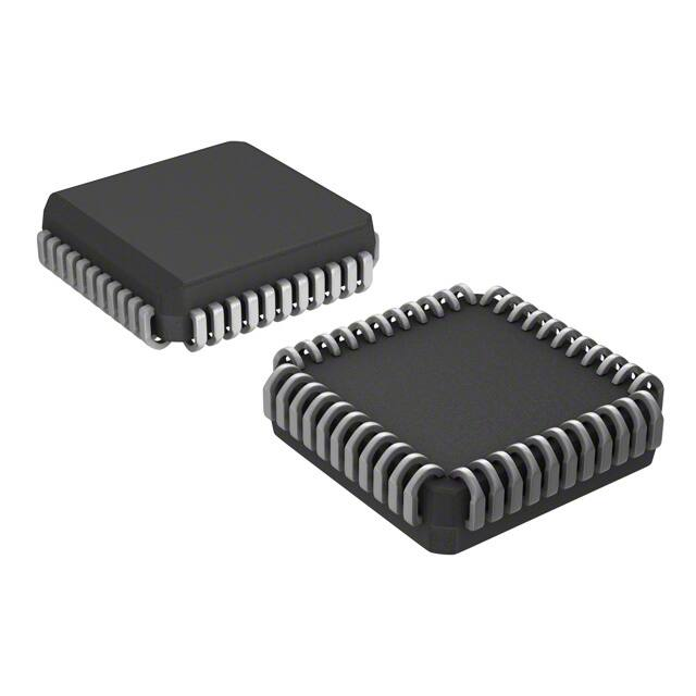


 工商网监
湘ICP备2023018690号
工商网监
湘ICP备2023018690号
