INTEGRATED CIRCUITS
74F827
10-bit buffer/line driver, non-inverting
(3-State)
Product data
Replaces Product specification 74F827/74F828 of 1994 Dec 5
�����
�����
����
�
2004 Jan 21
�Philips Semiconductors
Product data
10-bit buffer/line driver, non-inverting (3-State)
FEATURES
74F827
DESCRIPTION
• High impedance NPN base inputs for reduced loading (20 µA in
The 74F827 10-Bit buffer provides high performance bus interface
buffering for wide data/address paths or buses carrying parity. The
device has NOR Output Enables (OE0, OE1) for maximum control
flexibility.
HIGH and LOW states)
• IIL is 20 µA vs FAST family spec of 600 µA
• Ideal where high speed, light bus loading and increased fan-in are
required
• Controlled rise and fall times to minimize ground bounce
• Glitch free power-up in 3-State
• Flow through pinout architecture for microprocessor oriented
TYPE
TYPICAL
PROPAGATION DELAY
TYPICAL
SUPPLY CURRENT
(TOTAL)
74F827
6.0ns
60 mA
applications
• Outputs sink 64 mA
• 74F827 is available in SSOP type II package
ORDERING INFORMATION
COMMERCIAL RANGE: VCC = 5 V ± 10%; Tamb = 0 °C to +70 °C
Package
Type number
Name
Description
Version
N74F827N
DIP24
plastic dual in-line package; 24 leads (300 mil)
SOT222-1
N74F827D
SO24
plastic small outline package; 24 leads; body width 7.5 mm
SOT137-1
N74F827DB
SSOP24
plastic shrink small outline package; 24 leads; body width 5.3 mm
SOT340-1
INPUT AND OUTPUT LOADING AND FAN-OUT TABLE
74F(U.L.)
HIGH/LOW
LOAD VALUE
HIGH / LOW
Data inputs
1.0/0.033
20 µA / 20 µA
Output enable inputs (active-LOW)
1.0/0.033
20 µA / 20 µA
1200/106.7
24 mA / 64 mA
PINS
DESCRIPTION
D0-D9
OE0-OE1
Q0-Q9
Data outputs
NOTES:
One (1.0) FAST Unit Load is defined as: 20 µA in the HIGH state and 0.6 mA in the LOW state.
PIN CONFIGURATION
OE0
1
24 VCC
D0
2
23 Q0
D1
3
22 Q1
D2
4
21 Q2
D3
5
20 Q3
D4
6
19 Q4
D5
7
18 Q5
D6
8
17 Q6
D7
9
16 Q7
D8 10
15 Q8
D9 11
14 Q9
GND 12
13 OE1
SF00266
2004 Jan 21
2
�Philips Semiconductors
Product data
10-bit buffer/line driver, non-inverting (3-State)
LOGIC SYMBOL
74F827
LOGIC SYMBOL (IEEE/IEC)
1
2
3
4
5
6
7
8
9
&
13
EN1
2
1
10 11
D0 D1 D2 D3 D4 D5 D6 D7 D8 D9
23
3
22
1
OE0
4
21
13
OE1
5
20
6
19
7
18
8
17
9
16
Q0 Q1 Q2 Q3 Q4 Q5 Q6 Q7 Q8 Q9
23 22 21 20 19 18 17 16 15 14
VCC = Pin 24
GND = Pin 12
10
15
11
14
SF00267
SF00268
LOGIC DIAGRAM
D0
D1
D2
D3
D4
D5
D6
D7
2
3
4
5
6
7
8
9
D8
10
D9
11
1
OE0
13
OE1
23
22
Q1
Q0
21
Q2
20
19
Q3
Q4
VCC = Pin 24
GND = Pin 12
INPUTS
OUTPUTS
OPERATING MODE
OEn
Dn
Qn
L
L
L
Transparent
L
H
H
Transparent
X
Z
High impedance
H
=
=
=
=
HIGH voltage level
LOW voltage level
Don’t care
High impedance “off” state
2004 Jan 21
17
Q6
16
Q7
15
Q8
14
Q9
SF00272
FUNCTION TABLE
H
L
X
Z
18
Q5
3
�Philips Semiconductors
Product data
10-bit buffer/line driver, non-inverting (3-State)
74F827
ABSOLUTE MAXIMUM RATINGS
Operation beyond the limits set forth in this table may impair the useful life of the device.
Unless otherwise noted these limits are over the operating free-air temperature range.
SYMBOL
PARAMETER
RATING
UNIT
VCC
Supply voltage
–0.5 to +7.0
V
VIN
Input voltage
–0.5 to +7.0
V
IIN
Input current
–30 to +5
mA
–0.5 to +VCC
V
VOUT
Voltage applied to output in HIGH output state
IOUT
Current applied to output in LOW output state
Tamb
Operating free-air temperature range
Tstg
Storage temperature range
128
mA
0 to +70
°C
–65 to +150
°C
RECOMMENDED OPERATING CONDITIONS
LIMITS
SYMBOL
PARAMETER
UNIT
Min
Nom
Max
5.5
V
VCC
Supply voltage
4.5
5.0
VIH
HIGH-level input voltage
2.0
–
–
V
VIL
LOW-level input voltage
–
–
0.8
V
IIK
Input clamp current
–
–
–18
mA
IOH
HIGH-level output current
–
–
–24
mA
IOL
LOW-level output current
–
–
64
mA
Operating free-air temperature range
0
–
+70
°C
Tamb
2004 Jan 21
4
�Philips Semiconductors
Product data
10-bit buffer/line driver, non-inverting (3-State)
74F827
DC ELECTRICAL CHARACTERISTICS
Over recommended operating free-air temperature range unless otherwise noted.
SYMBOL
VOH
O
TEST CONDITIONS1
PARAMETER
HIGH level output voltage
HIGH-level
VCC = MIN,
VIL = MAX
MAX,
VIH = MIN
IOH
15 mA
O = –15
VCC = MIN,
VIL = MAX
MAX,
VIH = MIN
IOH
24 mA
O = –24
IOL
O = 64 mA
LIMITS
UNIT
MIN
TYP2
MAX
± 10% VCC
2.4
–
–
V
± 5% VCC
2.4
3.3
–
V
± 10% VCC
2.0
–
–
V
± 5% VCC
2.0
–
–
V
± 10% VCC
–
–
0.55
V
± 5% VCC
–
0.42
0.55
V
VOL
O
LOW level output voltage
LOW-level
VCC = MIN,
VIL = MAX
MAX,
VIH = MIN
VIK
Input clamp voltage
VCC = MIN; II = IIK
–
–0.73
–1.2
V
II
Input current at maximum input voltage
VCC = 0 V; VI = 7.0 V
–
–
100
µA
IIH
HIGH-level input current
VCC = MAX; VI = 2.7 V
–
–
20
µA
IIL
LOW-level input current
VCC = MAX; VI = 0.5 V
–
–
–20
µA
IOZH
Off-state output current,
HIGH voltage applied
VCC = MAX; VO = 2.7 V
–
–
50
µA
IOZL
Off-state output current,
LOW voltage applied
VCC = MAX; VO = 0.5 V
–
–
–50
µA
IOS
Short circuit output current 3
VCC = MAX
–100
–
–225
mA
–
50
70
mA
ICC
Supply current (total)
–
70
100
mA
–
60
90
mA
ICCH
ICCL
VCC = MAX
ICCZ
NOTES:
1. For conditions shown as MIN or MAX, use the appropriate value specified under operating conditions for the applicable type.
2. All typical values are at VCC = 5 V, Tamb = 25 °C.
3. Not more than one output should be shorted at one time. For testing IOS, the use of high-speed test apparatus and/or sample-and-hold
techniques are preferable in order to minimize internal heating and more accurately reflect operational values. Otherwise, prolonged
shorting of a HIGH output may raise the chip temperature well above normal and thereby cause invalid readings in other parameter tests.
In any sequence of parameter tests, IOS tests should be performed last.
2004 Jan 21
5
�Philips Semiconductors
Product data
10-bit buffer/line driver, non-inverting (3-State)
74F827
AC CHARACTERISTICS
LIMITS
SYMBOL
PARAMETER
Tamb = +25 °C
VCC = 5 V
CL = 50 pF; RL = 500 Ω
CONDITIONS
Tamb = 0 °C to +70 °C
VCC = 5 V ± 10%
CL = 50 pF; RL = 500 Ω
Min
Typ
Max
Min
Max
UNIT
tPLH
tPHL
Propagation delay
Dn to Qn
Waveform 1
2.0
2.0
5.5
4.5
8.5
8.5
2.0
2.0
9.0
9.0
ns
tPZH
tPZL
Output enable time
OEn to Qn
Waveform 2
Waveform 3
5.0
4.0
8.0
6.0
12.0
10.5
4.5
4.0
14.0
11.5
ns
tPHZ
tPLZ
Output disable time
OEn to Qn
Waveform 2
Waveform 3
2.5
2.5
5.0
5.0
8.0
8.0
2.0
2.0
8.5
8.5
ns
AC CHARACTERISTICS
For 1 Output switching with CL = 300 pF and RL = 500 Ω load
LIMITS
SYMBOL
PARAMETER
Tamb = +25 °C
VCC = 5 V
CL = 300 pF; RL = 500 Ω
CONDITIONS
Tamb = 0 °C to +70 °C
VCC = 5 V ± 10%
CL = 300 pF; RL = 500 Ω
MIN
Typ
Max
MIN
Max
UNIT
tPLH
tPHL
Propagation delay
Dn to Qn
Waveform 1
–
–
9.5
7.5
13.0
10.0
–
–
14.0
11.0
ns
tPZH
tPZL
Output enable time
OEn to Qn
Waveform 2
Waveform 3
–
–
15.0
9.5
20.0
13.0
–
–
21.0
14.0
ns
tPHZ
tPLZ
Output disable time
OEn to Qn
Waveform 2
Waveform 3
–
–
15.0
9.5
19.0
13.5
–
–
20.0
14.0
ns
AC CHARACTERISTICS
For 10 Outputs switching with CL = 300 pF and RL = 500 Ω load
LIMITS
SYMBOL
PARAMETER
Tamb = +25 °C
VCC = 5 V
CL = 300 pF; RL = 500 Ω
CONDITIONS
Tamb = 0 °C to +70 °C
VCC = 5 V ± 10%
CL = 300 pF; RL = 500 Ω
MIN
Typ
Max
MIN
Max
UNIT
tPLH
tPHL
Propagation delay
Dn to Qn
Waveform 1
–
–
12.0
14.0
16.0
17.0
–
–
17.0
18.0
ns
tPZH
tPZL
Output enable time
OEn to Qn
Waveform 2
Waveform 3
–
–
15.0
17.0
20.0
21.0
–
–
21.0
21.5
ns
tPHZ
tPLZ
Output disable time
OEn to Qn
Waveform 2
Waveform 3
–
–
15.0
12.5
19.0
15.5
–
–
20.0
16.0
ns
2004 Jan 21
6
�Philips Semiconductors
Product data
10-bit buffer/line driver, non-inverting (3-State)
74F827
AC WAVEFORMS
For all waveforms, VM = 1.5 V
Dn
VM
VM
tPLH
tPHL
Qn
VM
VM
SF00125
Waveform 1. Propagation delay for non-inverting output
OEn
VM
VM
tPZH
tPHZ
Qn, Qn
OEn
VM
VM
tPZL
VOH -0.3V
tPLZ
VM
Qn, Qn
VM
VOL +0.3V
0V
SF00263
SF00264
Waveform 2. 3-State Output Enable time to HIGH level
and Output Disable time from HIGH level
Waveform 3. 3-State Output Enable time to LOW level
and Output Disable time from LOW level
VCC
7.0 V
VIN
RL
VOUT
PULSE
GENERATOR
tw
90%
NEGATIVE
PULSE
VM
CL
AMP (V)
VM
10%
D.U.T.
RT
90%
10%
tTHL (tf )
tTLH (tr )
tTLH (tr )
tTHL (tf )
0V
RL
AMP (V)
90%
90%
Test Circuit for Open Collector Outputs
POSITIVE
PULSE
VM
VM
10%
TEST
tPLZ
tPZL
All other
SWITCH
closed
closed
open
DEFINITIONS:
RL = Load resistor;
see AC electrical characteristics for value.
CL = Load capacitance includes jig and probe capacitance;
see AC electrical characteristics for value.
RT = Termination resistance should be equal to ZOUT of
pulse generators.
10%
tw
SWITCH POSITION
0V
Input Pulse Definition
INPUT PULSE REQUIREMENTS
family
amplitude VM
74F
3.0 V
1.5 V
rep. rate
1 MHz
tw
tTLH
500 ns 2.5 ns
tTHL
2.5 ns
SF00128
2004 Jan 21
7
�Philips Semiconductors
Product data
10-bit buffer/line driver, non-inverting (3-State)
DIP24: plastic dual in-line package; 24 leads (300 mil)
2004 Jan 21
8
74F827
SOT222-1
�Philips Semiconductors
Product data
10-bit buffer/line driver, non-inverting (3-State)
SO24: plastic small outline package; 24 leads; body width 7.5 mm
2004 Jan 21
9
74F827
SOT137-1
�Philips Semiconductors
Product data
10-bit buffer/line driver, non-inverting (3-State)
SSOP24: plastic shrink small outline package; 24 leads; body width 5.3 mm
2004 Jan 21
10
74F827
SOT340-1
�Philips Semiconductors
Product data
10-bit buffer/line driver, non-inverting (3-State)
74F827
REVISION HISTORY
Rev
Date
Description
_3
20040121
Product data (9397 750 12741). ECN 853-0880 A15336 of 21 January 2004.
Replaces 74F827_74F828_2 dated 1994 Dec 5.
Modifications:
• Delete all references to 74F828 (product discontinued).
• AC Characteristics table (for 10 outputs switching): change Limits columns’ headings from CL = 50 pF to CL = 300 pF.
_2
19941205
Product specification. ECN 853-0880 14382 of 05 December 1994.
Data sheet status
Level
Data sheet status [1]
Product
status [2] [3]
Definitions
I
Objective data
Development
This data sheet contains data from the objective specification for product development.
Philips Semiconductors reserves the right to change the specification in any manner without notice.
II
Preliminary data
Qualification
This data sheet contains data from the preliminary specification. Supplementary data will be published
at a later date. Philips Semiconductors reserves the right to change the specification without notice, in
order to improve the design and supply the best possible product.
III
Product data
Production
This data sheet contains data from the product specification. Philips Semiconductors reserves the
right to make changes at any time in order to improve the design, manufacturing and supply. Relevant
changes will be communicated via a Customer Product/Process Change Notification (CPCN).
[1] Please consult the most recently issued data sheet before initiating or completing a design.
[2] The product status of the device(s) described in this data sheet may have changed since this data sheet was published. The latest information is available on the Internet at URL
http://www.semiconductors.philips.com.
[3] For data sheets describing multiple type numbers, the highest-level product status determines the data sheet status.
Definitions
Short-form specification — The data in a short-form specification is extracted from a full data sheet with the same type number and title. For detailed information see
the relevant data sheet or data handbook.
Limiting values definition — Limiting values given are in accordance with the Absolute Maximum Rating System (IEC 60134). Stress above one or more of the limiting
values may cause permanent damage to the device. These are stress ratings only and operation of the device at these or at any other conditions above those given
in the Characteristics sections of the specification is not implied. Exposure to limiting values for extended periods may affect device reliability.
Application information — Applications that are described herein for any of these products are for illustrative purposes only. Philips Semiconductors make no
representation or warranty that such applications will be suitable for the specified use without further testing or modification.
Disclaimers
Life support — These products are not designed for use in life support appliances, devices, or systems where malfunction of these products can reasonably be
expected to result in personal injury. Philips Semiconductors customers using or selling these products for use in such applications do so at their own risk and agree
to fully indemnify Philips Semiconductors for any damages resulting from such application.
Right to make changes — Philips Semiconductors reserves the right to make changes in the products—including circuits, standard cells, and/or software—described
or contained herein in order to improve design and/or performance. When the product is in full production (status ‘Production’), relevant changes will be communicated
via a Customer Product/Process Change Notification (CPCN). Philips Semiconductors assumes no responsibility or liability for the use of any of these products, conveys
no license or title under any patent, copyright, or mask work right to these products, and makes no representations or warranties that these products are free from patent,
copyright, or mask work right infringement, unless otherwise specified.
Koninklijke Philips Electronics N.V. 2004
All rights reserved. Printed in U.S.A.
Contact information
For additional information please visit
http://www.semiconductors.philips.com.
Fax: +31 40 27 24825
Date of release: 01-04
For sales offices addresses send e-mail to:
sales.addresses@www.semiconductors.philips.com.
Document order number:
�����
�����
����
�
2004 Jan 21
11
9397 750 12741
�
很抱歉,暂时无法提供与“N74F827DB,118”相匹配的价格&库存,您可以联系我们找货
免费人工找货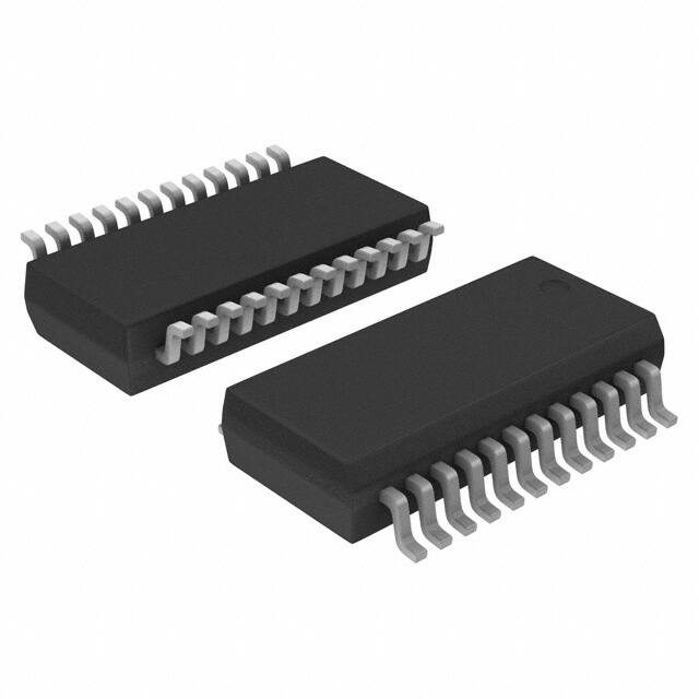


 工商网监
湘ICP备2023018690号
工商网监
湘ICP备2023018690号
