NX3L2267-Q100
Low-ohmic dual single-pole double-throw analog switch
Rev. 1 — 7 August 2012
Product data sheet
1. General description
The NX3L2267-Q100 is a dual low-ohmic single-pole double-throw analog switch suitable
for use as an analog or digital 2:1 multiplexer/demultiplexer. Each switch has a digital
select input (nS), two independent inputs/outputs (nY0 and nY1) and a common
input/output (nZ).
Schmitt trigger action at the digital inputs makes the circuit tolerant to slower input rise and
fall times. Low threshold digital inputs allows this device to be driven by 1.8 V logic levels
in 3.3 V applications without significant increase in supply current ICC. This makes it
possible for the NX3L2267-Q100 to switch 4.3 V signals with a 1.8 V digital controller,
eliminating the need for logic level translation. The NX3L2267-Q100 allows signals with
amplitude up to VCC to be transmitted from nZ to nY0 or nY1, or from nY0 or nY1 to nZ. Its
low ON resistance (0.5 ) and flatness (0.13 ) ensures minimal attenuation and
distortion of transmitted signals.
This product has been qualified to the Automotive Electronics Council (AEC) standard
Q100 (Grade 1) and is suitable for use in automotive applications.
2. Features and benefits
Automotive product qualification in accordance with AEC-Q100 (Grade 1)
Specified from 40 C to +85 C and from 40 C to +125 C
Wide supply voltage range from 1.4 V to 4.3 V
Very low ON resistance (peak):
1.65 (typical) at VCC = 1.4 V
0.95 (typical) at VCC = 1.65 V
0.55 (typical) at VCC = 2.3 V
0.50 (typical) at VCC = 2.7 V
0.50 (typical) at VCC = 4.3 V
Break-before-make switching
High noise immunity
ESD protection:
MIL-STD-883, method 3015 Class 3A exceeds 7500 V
HBM JESD22-A114F Class 3A exceeds 7500 V
MM JESD22-A115-A exceeds 200 V (C = 200 pF, R = 0 )
CDM AEC-Q100-011 revision B exceeds 1000 V
IEC61000-4-2 contact discharge exceeds 8000 V for switch ports
CMOS low-power consumption
Latch-up performance exceeds 100 mA per JESD 78B Class II Level A
�NX3L2267-Q100
NXP Semiconductors
Low-ohmic dual single-pole double-throw analog switch
1.8 V control logic at VCC = 3.6 V
Control input accepts voltages above supply voltage
Very low supply current, even when input is below VCC
High current handling capability (350 mA continuous current under 3.3 V supply)
3. Applications
Cell phone
PDA
Portable media player
4. Ordering information
Table 1.
Ordering information
Type number
Package
Temperature range Name
Description
Version
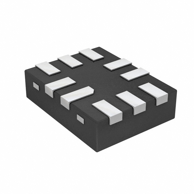
NX3L2267GM-Q100 40 C to +125 C
XQFN10
plastic extremely thin quad flat package; no leads;
10 terminals; body 1.55 2.00 0.50 mm
SOT1049-3
40 C to +125 C
XQFN10
plastic, extremely thin quad flat package; no leads;
10 terminals; body 1.40 1.80 0.50 mm
SOT1160-1
NX3L2267GU-Q100
5. Marking
Table 2.
Marking
Type number
Marking code
NX3L2267GM-Q100
M67
NX3L2267GU-Q100
M7
6. Functional diagram
Y1
1Y0
2Y0
1S
2S
1Z
2Z
1Y1
S
Y0
2Y1
001aac355
001aaj085
Fig 1.
Logic symbol
NX3L2267_Q100
Product data sheet
Z
Fig 2.
Logic diagram (one switch)
All information provided in this document is subject to legal disclaimers.
Rev. 1 — 7 August 2012
© NXP B.V. 2012. All rights reserved.
2 of 22
�NX3L2267-Q100
NXP Semiconductors
Low-ohmic dual single-pole double-throw analog switch
7. Pinning information
7.1 Pinning
�
很抱歉,暂时无法提供与“NX3L2267GU-Q100X”相匹配的价格&库存,您可以联系我们找货
免费人工找货