Ordering number : EN1719D
2SD1620
Bipolar Transistor
10V, 3A, Low VCE(sat), NPN Single PCP
http://onsemi.com
Features
Less power dissipation because of low VCE(sat), permitting more flashes of light to be emitted
Large current capacity and highly resistant to breakdown
Excellent linearity of hFE in the region from low current to high current
Ultrasmall size supports high-density, ultrasmall-sized hybrid IC designs
•
•
•
•
Specifications
Absolute Maximum Ratings at Ta=25°C
Parameter
Symbol
Collector-to-Base Voltage
Collector-to-Emitter Voltage
Collector-to-Emitter Voltage
Emitter-to-Base Voltage
Collector Current
Conditions
Ratings
Unit
VCBO
VCEX
30
V
20
V
VCEO
VEBO
10
V
IC
ICP
Collector Current (Pulse)
6
V
3
A
5
A
Continued on next page.
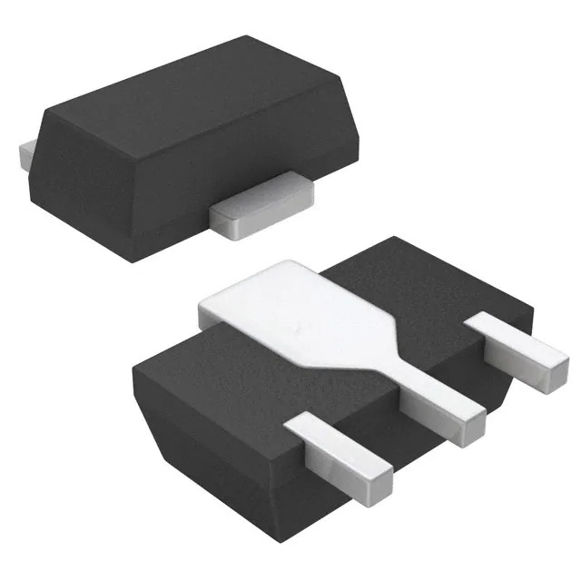
Package Dimensions
Product & Package Information
unit : mm (typ)
7007B-004
• Package
: PCP
• JEITA, JEDEC
: SC-62, SOT-89, TO-243
• Minimum Packing Quantity : 1,000 pcs./reel
Top View
2SD1620-TD-E
2.5
1.0
1
2
Packing Type: TD
4.0
1.5
TD
Marking
LOT No.
1.6
DC
4.5
3
0.4
0.4
0.5
1.5
3.0
Electrical Connection
2
0.75
1
1 : Base
2 : Collector
3 : Emitter
Bottom View
3
PCP
Semiconductor Components Industries, LLC, 2013
September, 2013
82212 TKIM/31010EA TKIM/31005TN(PC)/21599TH (KT)/N1596TS(KOTO)8-7707/5277KI/3045MW, TS No.1719-1/6
�2SD1620
Continued from preceding page.
Parameter
Symbol
Conditions
Ratings
Unit
500
Collector Dissipation
PC
Junction Temperature
Tj
Storage Temperature
Tstg
When mounted on ceramic substrate (250mm2×0.8mm)
mW
1.3
W
150
°C
--55 to +150
°C
Stresses exceeding Maximum Ratings may damage the device. Maximum Ratings are stress ratings only. Functional operation above the Recommended Operating
Conditions is not implied. Extended exposure to stresses above the Recommended Operating Conditions may affect device reliability.
Electrical Characteristics at Ta=25°C
Parameter
Symbol
Collector Cutoff Current
ICBO
IEBO
hFE
Emitter Cutoff Current
DC Current Gain
Gain-Bandwidth Product
Collector-to-Emitter Saturation Voltage
VCE(sat)
V(BR)CBO
Collector-to-Base Breakdown Voltage
Collector-to-Emitter Breakdown Voltage
min
Collector-to-Emitter Breakdown Voltage
V(BR)CEX
V(BR)CEO
Emitter-to-Base Breakdown Voltage
V(BR)EBO
typ
Unit
max
VCB=20V, IE=0A
100
nA
VEB=4V, IC=0A
100
nA
VCE=2V, IC=3A
fT
Cob
Output Capacitance
Ratings
Conditions
140
210
VCE=10V, IC=50mA
200
VCB=10V, f=1MHz
IC=3A, IB=60mA
30
MHz
pF
0.3
0.4
V
IC=10μA, IE=0A
IC=1mA, VBE=3V
30
V
20
V
IC=1mA, RBE=∞
IE=10μA, IC=0A
10
V
6
V
Ordering Information
Device
Package
Shipping
memo
PCP
1,000pcs./reel
Pb Free
2SD1620-TD-E
IC -- VCE
25mA
3
15mA
10mA
2
5mA
1
IB=0mA
0
0.2
0.4
0.6
0.8
4
25mA
15mA
3
10mA
2
5mA
1
2mA
0
mA
mA
A
40m
40
60
4
IC -- VCE
5
Collector Current, IC -- A
Collector Current, IC -- A
5
2mA
1mA
IB=0mA
0
1.0
Collector-to-Emitter Voltage, VCE -- V
1.2
ITR09987
0
5
6
Collector-to-Emitter Voltage, VCE -- V
1
2
3
4
ITR09988
No.1719-2/6
�2SD1620
IC -- VBE
3.2
hFE -- IC
1000
VCE=2V
7
2.4
5
DC Current Gain, hFE
Collector Current, IC -- A
VCE=2V
2.8
2.0
1.6
1.2
0.8
3
2
100
0.4
7
0
0
0.2
0.4
0.6
0.8
1.0
Base-to-Emitter Voltage, VBE -- V
5
0.01
1.2
3
5
2
0.1
3
5
2
1.0
f=1MHz
2
7
Output Capacitance, Cob -- pF
Gain-Bandwidth Product, f T -- MHz
5
10
ITR09990
Cob -- VCB
3
VCE=10V
5
3
2
100
100
7
5
3
2
7
5
10
2
3
5
7
2
100
3
5
Collector Current, IC -- mA
10
1.0
7 1000
ITR09991
IC / IB=50
Collector Current, IC -- A
7
ICP=5A
DC
1.0
tio
2
7
5
Single pulse
Tc=25°C
3
2
1.0
3
5
7 10
ITR09993
PC -- Ta
1.6
n
3
3
7
s
op
era
7
5
0.1
5
0m
2
5
Collector Current, IC -- A
10
IC=3A
3
s
100
5
ITR09992
m
2
3
s
3
2
10
10
5
7
1m
7
3
5
ASO
7
5
1000
2
3
10
2
2
0.1
2
Collector-to-Base Voltage, VCB -- V
VCE(sat) -- IC
3
Collector-to-Emitter
Saturation Voltage, VCE(sat) -- mV
3
Collector Current, IC -- A
f T -- IC
1000
2
ITR09989
3
5
7
1.0
2
3
5
7
10
2
3
Collector-to-Emitter Voltage, VCE -- V ITR09995
Collector Dissipation, PC -- W
1.4
M
ou
1.2
nt
1.0
ed
on
ac
er
am
ic
0.8
bo
ar
d(
25
0.6
No h
0m
m2
✕0
.8
eat s
0.4
ink
0.2
m
m
)
0
0
20
40
60
80
100
120
Ambient Temperature, Ta -- °C
140
160
ITR09994
No.1719-3/6
�2SD1620
Bag Packing Specification
2SD1620-TD-E
No.1719-4/6
�2SD1620
Outline Drawing
2SD1620-TD-E
Land Pattern Example
Mass (g) Unit
0.058 mm
* For reference
Unit: mm
0.9
2.2
3.7
45°
45°
1.0
1.8
1.5
1.0
1.5
3.0
No.1719-5/6
�2SD1620
ON Semiconductor and the ON logo are registered trademarks of Semiconductor Components Industries, LLC (SCILLC). SCILLC owns the rights to a number
of patents, trademarks, copyrights, trade secrets, and other intellectual property. A listing of SCILLC’s product/patent coverage may be accessed at
www.onsemi.com/site/pdf/Patent-Marking.pdf. SCILLC reserves the right to make changes without further notice to any products herein. SCILLC makes no
warranty, representation or guarantee regarding the suitability of its products for any particular purpose, nor does SCILLC assume any liability arising out of the
application or use of any product or circuit, and specifically disclaims any and all liability, including without limitation special, consequential or incidental
damages. “Typical” parameters which may be provided in SCILLC data sheets and/or specifications can and do vary in different applications and actual
performance may vary over time. All operating parameters, including “Typicals” must be validated for each customer application by customer’s technical
experts. SCILLC does not convey any license under its patent rights nor the rights of others. SCILLC products are not designed, intended, or authorized for use
as components in systems intended for surgical implant into the body, or other applications intended to support or sustain life, or for any other application in
which the failure of the SCILLC product could create a situation where personal injury or death may occur. Should Buyer purchase or use SCILLC products for
any such unintended or unauthorized application, Buyer shall indemnify and hold SCILLC and its officers, employees, subsidiaries, affiliates, and distributors
harmless against all claims, costs, damages, and expenses, and reasonable attorney fees arising out of, directly or indirectly, any claim of personal injury or
death associated with such unintended or unauthorized use, even if such claim alleges that SCILLC was negligent regarding the design or manufacture of the
part. SCILLC is an Equal Opportunity/Affirmative Action Employer. This literature is subject to all applicable copyright laws and is not for resale in any manner.
PS No.1719-6/6
�


 工商网监
湘ICP备2023018690号
工商网监
湘ICP备2023018690号
