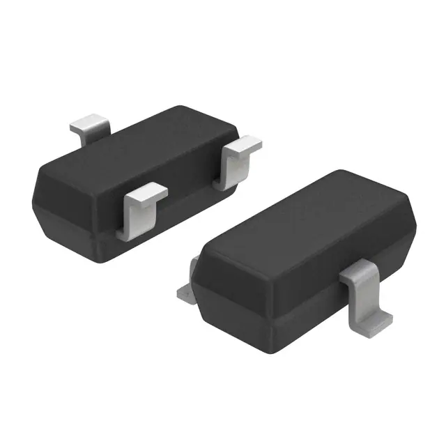
50A02CH
Bipolar Transistor
−50V, −0.5A, Low VCE(sat), PNP Single
www.onsemi.com
Features
• High Collector Current Capability
• Low Collector to Emitter Saturation Voltage (Resistance):
RCE(sat) typ=210mΩ [IC=0.5A, IB=50mA]
• Low ON-Resistance (Ron)
• Pb-Free, Halogen Free and RoHS compliance
ELECTRICAL CONNECTION
3
1 : Base
2 : Emitter
3 : Collector
1
Typical Applications
• Low-Frequency Amplifier
• High Speed Switching
• Small Motor Drive
• Muting Circuit
2
MARKING
© Semiconductor Components Industries, LLC, 2016
April 2016 - Rev. 2
1
1
2
CPH3
LOT No.
Parameter
Symbol
Value
Unit
Collector to Base Voltage
VCBO
−50
V
Collector to Emitter Voltage
VCEO
−50
V
Emitter to Base Voltage
VEBO
−5
V
Collector Current
IC
−500
mA
Collector Current (Pulse)
ICP
−1.0
A
Collector Dissipation (Note 2)
PC
700
mW
Junction Temperature
Tj
150
°C
Storage Temperature
Tstg
−55 to +150
°C
Note 1 : Stresses exceeding those listed in the Maximum Ratings table may damage
the device. If any of these limits are exceeded, device functionality should not
be assumed, damage may occur and reliability may be affected.
2
Note 2 : Surface mounted on ceramic substrate(600mm × 0.8mm)
AX
3
SPECIFICATIONS
ABSOLUTE MAXIMUM RATING at Ta = 25°C (Note 1, 2)
ORDERING INFORMATION
See detailed ordering and shipping
information on page 5 of this data sheet.
Publication Order Number :
50A02CH/D
�50A02CH
ELECTRICAL CHARACTERISTICS at Ta = 25°C (Note 3)
Parameter
Symbol
Conditions
Value
min
typ
max
Unit
Collector Cutoff Current
ICBO
VCB=−40V, IE=0A
−100
nA
Emitter Cutoff Current
IEBO
VEB=−4V, IC=0A
−100
nA
DC Current Gain
hFE
fT
VCE=−2V, IC=−10mA
Gain-Bandwidth Product
VCE=−10V, IC=−50mA
690
MHz
Output Capacitance
Cob
VCB=−10V, f=1MHz
3.8
pF
Collector to Emitter Saturation
Voltage
VCE(sat)
IC=−100mA, IB=−10mA
−60
−120
mV
Base to Emitter Saturation Voltage
VBE(sat)
IC=−100mA, IB=−10mA
−0.9
−1.2
V
V(BR)CBO
IC=−10μA, IE=0A
−50
V
V(BR)CEO
IC=−1mA, RBE=∞
−50
V
Emitter to Base Breakdown Voltage
V(BR)EBO
IE=−10μA, IC=0A
−5
Turn-On Time
ton
tstg
Collector to Base Breakdown
Voltage
Collector to Emitter Breakdown
Voltage
Storage Time
See specified Test
Circuit
200
500
V
30
ns
170
ns
Fall Time
30
tf
ns
Note 3 : Product parametric performance is indicated in the Electrical Characteristics for the listed test conditions, unless otherwise noted.
Product performance may not be indicated by the Electrical Characteristics if operated under different conditions.
Switching Time Test Circuit
www.onsemi.com
2
�50A02CH
www.onsemi.com
3
�50A02CH
www.onsemi.com
4
�50A02CH
PACKAGE DIMENSIONS
unit : mm
CPH3
CASE 318BA
ISSUE O
1 : Base
2 : Emitter
Recommended
Soldering Footprint
3 : Collector
2.4
1.4
0.6
0.95
0.95
ORDERING INFORMATION
Device
Marking
Package
CPH3
(Pb-Free)
50A02CH-TL-E
AX
50A02CH-TL-H
CPH3
(Pb-Free / Halogen Free)
Shipping (Qty / Packing)
3,000 / Tape & Reel
† For information on tape and reel specifications, including part orientation and tape sizes, please refer to our Tape and Reel Packaging Specifications
Brochure, BRD8011/D. http://www.onsemi.com/pub_link/Collateral/BRD8011-D.PDF
ON Semiconductor and the ON logo are registered trademarks of Semiconductor Components Industries, LLC (SCILLC) or its subsidiaries in the United States
and/or other countries. SCILLC owns the rights to a number of patents, trademarks, copyrights, trade secrets, and other intellectual property. A listing of
SCILLC’s product/patent coverage may be accessed at www.onsemi.com/site/pdf/Patent-Marking.pdf . SCILLC reserves the right to make changes without
further notice to any products herein. SCILLC makes no warranty, representation or guarantee regarding the suitability of its products for any particular purpose,
nor does SCILLC assume any liability arising out of the application or use of any product or circuit, and specifically disclaims any and all liability, including
without limitation special, consequential or incidental damages. “Typical” parameters which may be provided in SCILLC data sheets and/or specifications can
and do vary in different applications and actual performance may vary over time. All operating parameters, including “Typicals” must be validated for each
customer application by customer’s technical experts. SCILLC does not convey any license under its patent rights nor the rights of others. SCILLC products are
not designed, intended, or authorized for use as components in systems intended for surgical implant into the body, or other applications intended to support or
sustain life, or for any other application in which the failure of the SCILLC product could create a situation where personal injury or death may occur. Should
Buyer purchase or use SCILLC products for any such unintended or unauthorized application, Buyer shall indemnify and hold SCILLC and its officers,
employees, subsidiaries, affiliates, and distributors harmless against all claims, costs, damages, and expenses, and reasonable attorney fees arising out of,
directly or indirectly, any claim of personal injury or death associated with such unintended or unauthorized use, even if such claim alleges that SCILLC was
negligent regarding the design or manufacture of the part. SCILLC is an Equal Opportunity/Affirmative Action Employer. This literature is subject to all
applicable copyright laws and is not for resale in any manner.
www.onsemi.com
5
�


 工商网监
湘ICP备2023018690号
工商网监
湘ICP备2023018690号
