74F11
Triple 3-Input AND Gate
tm
General Description
This device contains three independent gates, each of
which performs the logic AND function.
Ordering Information
Order
Number
Package
Number
Package Description
74F11SC
M14A
14-Lead Small Outline Integrated Circuit (SOIC), JEDEC MS-012, 0.150" Narrow
74F11SJ
M14D
14-Lead Small Outline Package (SOP), EIAJ TYPE II, 5.3mm Wide
Devices also available in Tape and Reel. Specify by appending the suffix letter “X” to the ordering number.
Connection Diagram
Logic Symbol
IEEE/IEC
Unit Loading/Fan Out
Pin Names
An, Bn, Cn
On
©1988 Fairchild Semiconductor Corporation
74F11 Rev. 1.3
Description
U.L.
HIGH/LOW
Input IIH/IIL,
Output IOH/IOL
Inputs
1.0 / 1.0
20 µA / –0.6mA
Outputs
50 / 33.3
–1 mA / 20 mA
www.fairchildsemi.com
74F11 Triple 3-Input AND Gate
May 2007
�Stresses exceeding the absolute maximum ratings may damage the device. The device may not function or be
operable above the recommended operating conditions and stressing the parts to these levels is not recommended.
In addition, extended exposure to stresses above the recommended operating conditions may affect device reliability.
The absolute maximum ratings are stress ratings only.
Symbol
TSTG
Parameter
Rating
Storage Temperature
–65°C to +150°C
TA
Ambient Temperature Under Bias
–55°C to +125°C
TJ
Junction Temperature Under Bias
–55°C to +150°C
VCC
VCC Pin Potential to Ground Pin
–0.5V to +7.0V
VIN
Input Voltage(1)
–0.5V to +7.0V
IIN
Input Current(1)
–30mA to +5.0mA
VO
Voltage Applied to Output in HIGH State (with VCC = 0V)
Standard Output
–0.5V to VCC
3-STATE Output
–0.5V to 5.5V
Current Applied to Output in LOW State (Max.)
twice the rated IOL (mA)
Note:
1. Either voltage limit or current limit is sufficient to protect inputs.
Recommended Operating Conditions
The Recommended Operating Conditions table defines the conditions for actual device operation. Recommended
operating conditions are specified to ensure optimal performance to the datasheet specifications. Fairchild does not
recommend exceeding them or designing to absolute maximum ratings.
Symbol
TA
VCC
Parameter
Rating
Free Air Ambient Temperature
0°C to +70°C
Supply Voltage
©1988 Fairchild Semiconductor Corporation
74F11 Rev. 1.3
+4.5V to +5.5V
www.fairchildsemi.com
2
74F11 Triple 3-Input AND Gate
Absolute Maximum Ratings
�Symbol
Parameter
VCC
Conditions
Min.
Typ.
Max.
2.0
Units
V
VIH
Input HIGH Voltage
Recognized as a HIGH
Signal
VIL
Input LOW Voltage
Recognized as a LOW
Signal
0.8
V
VCD
Input Clamp Diode Voltage
Min.
IIN = –18mA
–1.2
V
VOH
Output HIGH Voltage
Min.
IOH = –1mA
2.5
IOH = –1mA
2.7
VOL
Output LOW Voltage
IIH
10% VCC
5% VCC
V
Min.
IOL = 20mA
0.5
V
Input HIGH Current
Max.
VIN = 2.7V
5.0
µA
IBVI
Input HIGH Current Breakdown
Test
Max.
VIN = 7.0V
7.0
µA
ICEX
Output HIGH Leakage Current
Max.
VOUT = VCC
50
µA
VID
Input Leakage Test
0.0
IID = 1.9µA, All other pins
grounded
IOD
Output Leakage Circuit Current
0.0
VIOD = 150mV, All other
pins grounded
3.75
µA
IIL
Input LOW Current
VIN = 0.5V
–0.6
mA
10% VCC
Max.
4.75
V
IOS
Output Short-Circuit Current
Max.
VOUT = 0V
–150
mA
ICCH
Power Supply Current
Max.
VO = HIGH
4.1
6.2
mA
ICCL
Power Supply Current
Max.
VO = LOW
6.5
9.7
mA
–60
AC Electrical Characteristics
TA = +25°C,
VCC = +5.0V,
CL = 50pF
Symbol
tPLH
tPHL
Parameter
Propagation Delay,
An, Bn, Cn to On
©1988 Fairchild Semiconductor Corporation
74F11 Rev. 1.3
TA –55°C to +125°C,
VCC = +5.0V,
CL = 50pF
Min. Typ. Max.
Min.
Max.
TA = 0°C to +70°C,
VCC = +5.0V,
CL = 50pF
Min.
Max.
Units
ns
3.0
4.2
5.6
2.5
7.5
3.0
6.6
2.5
4.1
5.5
2.0
7.5
2.5
6.5
www.fairchildsemi.com
3
74F11 Triple 3-Input AND Gate
DC Electrical Characteristics
�74F11 Triple 3-Input AND Gate
Physical Dimensions
Dimensions are in millimeters unless otherwise noted.
Figure 1. 14-Lead Small Outline Integrated Circuit (SOIC), JEDEC MS-012, 0.150" Narrow
Package Number M14A
©1988 Fairchild Semiconductor Corporation
74F11 Rev. 1.3
www.fairchildsemi.com
4
�74F11 Triple 3-Input AND Gate
Physical Dimensions (Continued)
Dimensions are in millimeters unless otherwise noted.
Figure 2. 14-Lead Small Outline Package (SOP), EIAJ TYPE II, 5.3mm Wide
Package Number M14D
©1988 Fairchild Semiconductor Corporation
74F11 Rev. 1.3
www.fairchildsemi.com
5
�®
ACEx
Across the board. Around the world.™
ActiveArray™
Bottomless™
Build it Now™
CoolFET™
CROSSVOLT™
CTL™
Current Transfer Logic™
DOME™
2
E CMOS™
®
EcoSPARK
EnSigna™
FACT Quiet Series™
®
FACT
®
FAST
FASTr™
FPS™
®
FRFET
GlobalOptoisolator™
GTO™
HiSeC™
i-Lo™
ImpliedDisconnect™
IntelliMAX™
ISOPLANAR™
MICROCOUPLER™
MicroPak™
MICROWIRE™
Motion-SPM™
MSX™
MSXPro™
OCX™
OCXPro™
®
OPTOLOGIC
®
OPTOPLANAR
PACMAN™
PDP-SPM™
POP™
®
Power220
®
Power247
PowerEdge™
PowerSaver™
Power-SPM™
®
PowerTrench
Programmable Active Droop™
®
QFET
QS™
QT Optoelectronics™
Quiet Series™
RapidConfigure™
RapidConnect™
ScalarPump™
SMART START™
®
SPM
STEALTH™
SuperFET™
SuperSOT™-3
SuperSOT™-6
SuperSOT™-8
SyncFET™
TCM™
®
The Power Franchise
TinyBoost™
TinyBuck™
®
TinyLogic
TINYOPTO™
TinyPower™
TinyWire™
TruTranslation™
µSerDes™
®
UHC
UniFET™
VCX™
Wire™
™
DISCLAIMER
FAIRCHILD SEMICONDUCTOR RESERVES THE RIGHT TO MAKE CHANGES WITHOUT FURTHER NOTICE TO ANY PRODUCTS
HEREIN TO IMPROVE RELIABILITY, FUNCTION OR DESIGN. FAIRCHILD DOES NOT ASSUME ANY LIABILITY ARISING OUT OF THE
APPLICATION OR USE OF ANY PRODUCT OR CIRCUIT DESCRIBED HEREIN; NEITHER DOES IT CONVEY ANY LICENSE UNDER
ITS PATENT RIGHTS, NOR THE RIGHTS OF OTHERS. THESE SPECIFICATIONS DO NOT EXPAND THE TERMS OF FAIRCHILD’S
WORLDWIDE TERMS AND CONDITIONS, SPECIFICALLY THE WARRANTY THEREIN, WHICH COVERS THESE PRODUCTS.
LIFE SUPPORT POLICY
FAIRCHILD’S PRODUCTS ARE NOT AUTHORIZED FOR USE AS CRITICAL COMPONENTS IN LIFE SUPPORT DEVICES OR
SYSTEMS WITHOUT THE EXPRESS WRITTEN APPROVAL OF FAIRCHILD SEMICONDUCTOR CORPORATION.
As used herein:
1. Life support devices or systems are devices or systems
which, (a) are intended for surgical implant into the body or
(b) support or sustain life, and (c) whose failure to perform
when properly used in accordance with instructions for use
provided in the labeling, can be reasonably expected to
result in a significant injury of the user.
2. A critical component in any component of a life support,
device, or system whose failure to perform can be
reasonably expected to cause the failure of the life support
device or system, or to affect its safety or effectiveness.
PRODUCT STATUS DEFINITIONS
Definition of Terms
Datasheet Identification
Product Status
Advance Information
Formative or In Design
This datasheet contains the design specifications for product
development. Specifications may change in any manner without notice.
Definition
Preliminary
First Production
This datasheet contains preliminary data; supplementary data will be
published at a later date. Fairchild Semiconductor reserves the right to
make changes at any time without notice to improve design.
No Identification Needed
Full Production
This datasheet contains final specifications. Fairchild Semiconductor
reserves the right to make changes at any time without notice to improve
design.
Obsolete
Not In Production
This datasheet contains specifications on a product that has been
discontinued by Fairchild Semiconductor. The datasheet is printed for
reference information only.
Rev. I26
©1988 Fairchild Semiconductor Corporation
74F11 Rev. 1.3
www.fairchildsemi.com
6
74F11 Triple 3-Input AND Gate
TRADEMARKS
The following are registered and unregistered trademarks Fairchild Semiconductor owns or is authorized to use and is not intended to be an
exhaustive list of all such trademarks.
�
很抱歉,暂时无法提供与“74F11SC”相匹配的价格&库存,您可以联系我们找货
免费人工找货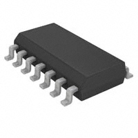


 工商网监
湘ICP备2023018690号
工商网监
湘ICP备2023018690号
