Revised September 2000
74F151A
8-Input Multiplexer
General Description
The F151A is a high-speed 8-input digital multiplexer. It
provides in one package the ability to select one line of
data from up to eight sources. The F151A can be used as a
universal function generator to generate any logic function
of four variables. Both assertion and negation outputs are
provided.
Ordering Code:
Order Number
Package Number
Package Description
74F151ASC
M16A
16-Lead Small Outline Integrated Circuit (SOIC), JEDEC MS-012, 0.150 Narrow
74F151ASJ
M16D
16-Lead Small Outline Package (SOP), EIAJ TYPE II, 5.3mm Wide
74F151APC
N16E
16-Lead Plastic Dual-In-Line Package (PDIP), JEDEC MS-001, 0.300 Wide
Devices also available in Tape and Reel. Specify by appending the suffix letter “X” to the ordering code.
Logic Symbols
Connection Diagram
IEEE/IEC
Unit Loading/Fan Out
U.L.
Pin Names
Description
Input IIH/IIL
HIGH/LOW Output IOH/IOL
I0–I7
Data Inputs
1.0/1.0
20 µA/−0.6 mA
S0–S2
Select Inputs
1.0/1.0
20 µA/−0.6 mA
E
Enable Input (Active LOW)
1.0/1.0
20 µA/−0.6 mA
Z
Data Output
50/33.3
−1 mA/20 mA
Z
Inverted Data Output
50/33.3
−1 mA/20 mA
© 2000 Fairchild Semiconductor Corporation
DS009481
www.fairchildsemi.com
74F151A 8-Input Multiplexer
April 1988
�74F151A
Functional Description
Truth Table
The F151A is a logic implementation of a single pole, 8position switch with the switch position controlled by the
state of three Select inputs, S0, S1, S2. Both assertion and
negation outputs are provided. The Enable input (E) is
active LOW. When it is not activated, the negation output is
HIGH and the assertion output is LOW regardless of all
other inputs. The logic function provided at the output is:
Inputs
Z = E • (I0 S2 S1 S0 + I1 S2 S1 S0 + I2 S2 S1 S0 +
I3 S2 S1 S0 + I4 S2 S1 S0 + I5 S2 S1 S0 +
Outputs
E
S2
S1
S0
Z
H
X
X
X
H
L
L
L
L
L
I0
I0
L
L
L
H
I1
I1
L
L
H
L
I2
I2
L
L
H
H
I3
I3
L
H
L
L
I4
I4
L
H
L
H
I5
I5
L
H
H
L
I6
I6
L
H
H
H
I7
I7
Z
I6 S2 S1 S0 + I7 S2 S1 S0)
The F151A provides the ability, in one package, to select
from eight sources of data or control information. By proper
manipulation of the inputs, the F151A can provide any logic
function of four variables and its negation.
H = HIGH Voltage Level
L = LOW Voltage Level
X = Immaterial
Logic Diagram
Please note that this diagram is provided only for the understanding of logic operations and should not be used to estimate propagation delays.
www.fairchildsemi.com
2
�Recommended Operating
Conditions
Storage Temperature
−65°C to +150°C
Ambient Temperature under Bias
−55°C to +125°C
Free Air Ambient Temperature
Junction Temperature under Bias
−55°C to +150°C
Supply Voltage
0°C to +70°C
+4.5V to +5.5V
VCC Pin Potential to
−0.5V to +7.0V
Ground Pin
Input Voltage (Note 2)
−0.5V to +7.0V
Input Current (Note 2)
−30 mA to +5.0 mA
Voltage Applied to Output
in HIGH State (with VCC = 0V)
Standard Output
−0.5V to VCC
3-STATE Output
−0.5V to +5.5V
Note 1: Absolute maximum ratings are values beyond which the device
may be damaged or have its useful life impaired. Functional operation
under these conditions is not implied.
Current Applied to Output
in LOW State (Max)
twice the rated IOL (mA)
Note 2: Either voltage limit or current limit is sufficient to protect inputs.
DC Electrical Characteristics
Symbol
Min
Parameter
Typ
Max
2.0
Units
VIH
Input HIGH Voltage
VIL
Input LOW Voltage
0.8
V
VCD
Input Clamp Diode Voltage
−1.2
V
VOH
Output HIGH
10% VCC
2.5
Voltage
5% VCC
2.7
VOL
Output LOW Voltage
10% VCC
IIH
Input HIGH Current
IBVI
Input HIGH Current
Breakdown Test
ICEX
Output HIGH
Leakage Current
VID
Input Leakage
Test
IOD
Circuit Current
Input LOW Current
IOS
Output Short-Circuit Current
ICC
Power Supply Current
−60
13.5
3
Conditions
Recognized as a HIGH Signal
Recognized as a LOW Signal
Min
IIN = −18 mA
IOH = −1 mA
V
Min
0.5
V
Min
IOL = 20 mA
5.0
µA
Max
VIN = 2.7V
7.0
µA
Max
VIN = 7.0V
50
µA
Max
VOUT = VCC
V
0.0
3.75
µA
0.0
−0.6
mA
Max
VIN = 0.5V
−150
mA
Max
VOUT = 0V
21.0
mA
Max
VO = HIGH
4.75
Output Leakage
IIL
VCC
V
IOH = −1 mA
IID = 1.9 µA
All Other Pins Grounded
VIOD = 150 mV
All Other Pins Grounded
www.fairchildsemi.com
74F151A
Absolute Maximum Ratings(Note 1)
�74F151A
AC Electrical Characteristics
Symbol
Parameter
TA = +25°C
TA = 0°C to +70°C
VCC = +5.0V
CL = 50 pF
CL = 50 pF
Min
Typ
Max
Min
Max
tPLH
Propagation Delay
4.0
6.2
9.0
3.5
9.5
tPHL
Sn to Z
3.2
5.2
7.5
3.2
7.5
tPLH
Propagation Delay
4.5
7.5
10.5
4.5
12.0
tPHL
Sn to Z
4.0
6.2
9.0
4.0
9.0
tPLH
Propagation Delay
3.0
4.7
6.1
3.0
7.0
tPHL
E to Z
3.0
4.4
6.0
2.5
6.0
tPLH
Propagation Delay
5.0
7.0
9.5
4.0
10.5
tPHL
E to Z
3.5
5.3
7.0
3.0
7.5
tPLH
Propagation Delay
3.0
4.8
6.5
3.0
7.0
tPHL
In to Z
1.5
2.5
4.0
1.5
5.0
tPLH
Propagation Delay
3.0
4.8
6.5
2.5
7.5
tPHL
In to Z
3.7
5.5
7.0
3.7
7.5
www.fairchildsemi.com
4
Units
ns
ns
ns
ns
ns
ns
�74F151A
Physical Dimensions inches (millimeters) unless otherwise noted
16-Lead Small Outline Integrated Circuit (SOIC), JEDEC MS-012, 0.150 Narrow
Package Number M16A
5
www.fairchildsemi.com
�74F151A
Physical Dimensions inches (millimeters) unless otherwise noted (Continued)
16-Lead Small Outline Package (SOP), EIAJ TYPE II, 5.3mm Wide
Package Number M16D
www.fairchildsemi.com
6
�74F151A 8-Input Multiplexer
Physical Dimensions inches (millimeters) unless otherwise noted (Continued)
16-Lead Plastic Dual-In-Line Package (PDIP), JEDEC MS-001, 0.300 Wide
Package Number N16E
Fairchild does not assume any responsibility for use of any circuitry described, no circuit patent licenses are implied and
Fairchild reserves the right at any time without notice to change said circuitry and specifications.
LIFE SUPPORT POLICY
FAIRCHILD’S PRODUCTS ARE NOT AUTHORIZED FOR USE AS CRITICAL COMPONENTS IN LIFE SUPPORT
DEVICES OR SYSTEMS WITHOUT THE EXPRESS WRITTEN APPROVAL OF THE PRESIDENT OF FAIRCHILD
SEMICONDUCTOR CORPORATION. As used herein:
2. A critical component in any component of a life support
device or system whose failure to perform can be reasonably expected to cause the failure of the life support
device or system, or to affect its safety or effectiveness.
1. Life support devices or systems are devices or systems
which, (a) are intended for surgical implant into the
body, or (b) support or sustain life, and (c) whose failure
to perform when properly used in accordance with
instructions for use provided in the labeling, can be reasonably expected to result in a significant injury to the
user.
www.fairchildsemi.com
7
www.fairchildsemi.com
�
很抱歉,暂时无法提供与“74F151APC”相匹配的价格&库存,您可以联系我们找货
免费人工找货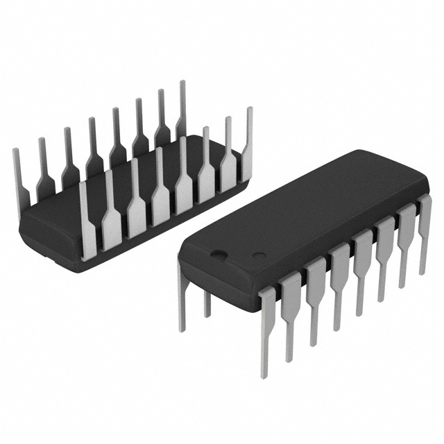


 工商网监
湘ICP备2023018690号
工商网监
湘ICP备2023018690号
