Revised January 2004
74F181
4-Bit Arithmetic Logic Unit
General Description
Features
The 74F181 is a 4-bit Arithmetic logic Unit (ALU) which can
perform all the possible 16 logic operations on two variables and a variety of arithmetic operations. It is 40% faster
than the Schottky ALU and only consumes 30% as much
power.
■ Full lookahead for high-speed arithmetic operation on
long words
Ordering Code:
Order Number
Package Number
Package Description
74F181PC
N24A
24-Lead Plastic Dual-In-Line Package (PDIP), JEDEC MS-011, 0.600" Wide
74F181SPC
N24C
24-Lead Plastic Dual-In-Line Package (PDIP), JEDEC MS-001, 0.300" Wide
Logic Symbols
Connection Diagram
Active-HIGH Operands
Active-LOW Operands
IEEE/IEC
© 2004 Fairchild Semiconductor Corporation
DS009491
www.fairchildsemi.com
74F181 4-Bit Arithmetic Logic Unit
April 1988
�74F181
Unit Loading/Fan Out
Pin Names
U.L.
Input IIH/IIL
HIGH/LOW
Output IOH/IOL
1.0/3.0
20 µA/−1.8 mA
Description
A0–A3
A Operand Inputs (Active LOW)
B0–B3
B Operand Inputs (Active LOW)
1.0/3.0
20 µA/−1.8 mA
S0–S3
Function Select Inputs
1.0/4.0
20 µA/−2.4 mA
M
Mode Control Input
1.0/1.0
20 µA/−0.6 mA
Cn
Carry Input
1.0/5.0
20 µA/−3.0 mA
50/33.3
−1 mA/20 mA
OC (Note 1)/33.3
(Note 1)/20 mA
Carry Generate Output (Active LOW)
50/33.3
−1 mA/20 mA
Carry Propagate Output (Active LOW)
50/33.3
−1 mA/20 mA
Carry Output
50/33.3
−1 mA/20 mA
F0–F3
Function Outputs (Active LOW)
A=B
Comparator Output
G
P
Cn + 4
Note 1: OC-Open Collector
Functional Description
devices. Carry lookahead can be provided at various levels
and offers high speed capability over extremely long word
lengths.
The 74F181 is a 4-bit high-speed parallel Arithmetic Logic
Unit (ALU). Controlled by the four Function Select inputs
(S0–S3) and the Mode Control input (M), it can perform all
the 16 possible logic operations or 16 different arithmetic
operations on Active HIGH or Active LOW operands. The
Function Table lists these operations.
The A = B output from the device goes HIGH when all four
F outputs are HIGH and can be used to indicate logic
equivalence over four bits when the unit is in the Subtract
mode. The A = B output is open collector and can be wired
AND with other A = B outputs to give a comparison for
more than four bits. The A = B signal can also be used with
the Cn+4 signal to indicate A > B and A < B.
When the Mode Control input (M) is HIGH, all internal carries are inhibited and the device performs logic operations
on the individual bits as listed. When the Mode Control
input is LOW, the carries are enabled and the device performs arithmetic operations on the two 4-bit words. The
device incorporates full internal carry lookahead and provides for either ripple carry between devices using the
Cn + 4 output, or for carry lookahead between packages
using the signals P (Carry Propagate) and G (Carry Generate). In the Add mode, P indicates that F is 15 or more,
while G indicates that F is 16 or more. In the Subtract mode
P indicates that F is zero or less, while G indicates that F is
less than zero. P and G are not affected by carry in. When
speed requirements are not stringent, the 74F181 can be
used in a simple Ripple Carry mode by connecting the
Carry output (Cn+4) signal to the Carry input (Cn) of the
next unit. For high speed operation the device is used in
conjunction with a carry lookahead circuit. One carry lookahead package is required for each group of four 74F181
www.fairchildsemi.com
The Function Table lists the arithmetic operations that are
performed without a carry in. An incoming carry adds a one
to each operation. Thus, select code LHHL generates A
minus B minus 1 (2s complement notation) without a carry
in and generates A minus B when a carry is applied.
Because subtraction is actually performed by complementary addition (1s complement), a carry out means borrow;
thus a carry is generated when there is no underflow and
no carry is generated when there is underflow. As indicated, this device can be used with either active LOW
inputs producing active LOW outputs or with active HIGH
inputs producing active HIGH outputs. For either case the
table lists the operations that are performed to the operands labeled inside the logic symbol.
2
�S0
a. All Input Data Inverted
b. All Input Data True
S1
S2
S3
Logic
Arithmetic
Arithmetic
(M=H)
(M=L, C0=Inactive)
(M=L, C0=Active)
L
L
L
L
A
A minus 1
A
H
L
L
L
A•B
A • B minus 1
A•B
A+B
A • B minus 1
A•B
L
H
L
L
H
H
L
L
L
L
H
L
H
L
H
L
L
H
H
L
H
H
H
L
Logic “1” minus 1 (2s comp.)
A+B
Zero
A plus (A + B)
A plus (A + B) plus 1
B
A • B plus (A + B)
A • B plus (A + B) plus 1
A⊕B
A minus B minus 1
A minus B
A+B
A+B
A + B plus 1
A plus (A + B plus 1
L
L
L
H
A•B
A plus (A + B)
H
L
L
H
A⊕ B
A plus B
A plus B plus 1
L
H
L
H
B
A • B plus (A + B)
A • B plus (A + B) plus 1
H
H
L
H
A+B
A+B
A + B plus 1
L
L
H
H
Logic “0”
A plus A (2 × A)
A plus A (2 × A) plus 1
H
L
H
H
A•B
A plus A • B
A plus A • B plus 1
L
H
H
H
A•B
A plus A • B
A plus A • B plus 1
H
H
H
H
A
A
A plus 1
L
L
L
L
A
A
A plus 1
H
L
L
L
A+B
A+B
A + B plus 1
L
H
L
L
A•B
A+B
A + B plus 1
H
H
L
L
L
L
H
L
Logic “0” minus 1 (2s comp.)
A•B
Zero
A plus (A • B)
A plus A • B plus 1
H
L
H
L
B
A • B plus (A + B)
A • B plus (A + B) plus 1
L
H
H
L
A⊕B
A minus B minus 1
A minus B
H
H
H
L
A•B
A • B minus 1
A•B
L
L
L
H
A+B
A plus A • B
A plus A • B plus 1
H
L
L
H
A⊕ B
A plus B
A plus B plus 1
L
H
L
H
B
A • B plus (A + B)
A • B plus (A + B) plus 1
H
H
L
H
A•B
A • B minus 1
A•B
L
L
H
H
Logic “1”
A plus A (2 × A)
A plus A (2 × A) plus 1
H
L
H
H
A+B
A plus (A + B)
A plus (A+B) plus 1
L
H
H
H
A+B
A plus (A + B)
A plus (A+B) plus 1
H
H
H
H
A
A minus 1
A
3
www.fairchildsemi.com
74F181
Operation Table
�74F181
Operation Table
(Continued)
S0
c. A All Input Data Inverted; B Input Data True
d. A Input Data True; B Input Date Inverted
www.fairchildsemi.com
S1
S2
S3
Logic
Arithmetic
Arithmetic
(M=H)
(M=L, C0=Inactive)
(M=L, C0=Active)
L
L
L
L
A
A minus 1
A
H
L
L
L
A+B
A • B minus 1
A•B
A•B
A • B minus 1
A•B
L
H
L
L
H
H
L
L
L
L
H
L
H
L
H
L
H
H
H
H
L
L
Logic “1” minus 1 (2s comp.)
Zero
A•B
A plus (A + B)
A plus (A + B) plus 1
L
B
A • B plus (A + B)
A • B plus (A + B) plus 1
L
A⊕B
A plus B
A plus B plus 1
H
L
A+B
A+B
A + B plus 1
L
H
A+B
A plus (A + B)
A plus (A + B) plus 1
H
L
L
H
A⊕ B
A minus B minus 1
A minus B
L
H
L
H
B
A • B plus (A + B)
A • B plus (A + B) plus 1
H
H
L
H
A+B
A+B
A + B plus 1
L
L
H
H
Logic “0”
A plus A (2 × A)
A plus A (2 × A) plus 1
H
L
H
H
A•B
A plus A • B
A plus A • B plus 1
L
H
H
H
A•B
A plus A • B
A plus A • B plus 1
H
H
H
H
A
A
A plus 1
L
L
L
L
A
A
A plus 1
H
L
L
L
A•B
A+B
A + B plus 1
A+B
A+B
A + B plus 1
L
H
L
L
H
H
L
L
L
L
H
L
H
L
H
L
H
H
H
H
L
L
Logic “0” minus 1 (2s comp.)
Zero
A+B
A plus A • B
A plus A • B plus 1
L
B
A • B plus (A + B)
A • B plus (A + B) plus 1
L
A⊕B
A plus B
A plus B plus 1
H
L
A•B
A • B minus 1
A•B
L
H
A•B
A plus A • B
A plus A • B plus 1
H
L
L
H
A⊕ B
A minus B minus 1
A minus B
L
H
L
H
B
A • B plus (A + B)
A • B plus (A + B) plus 1
H
H
L
H
A•B
A • B minus 1
A•B
L
L
H
H
Logic “1”
A plus A (2 × A)
A plus A (2 × A) plus 1
H
L
H
H
A+B
A plus (A + B)
A plus (A+B) plus 1
L
H
H
H
A+B
A plus (A + B)
A plus (A+B) plus 1
H
H
H
H
A
A minus 1
A
4
�74F181
Logic Diagram
p
Please note that this diagram is provided only for the understanding of logic operations and should not be used to estimate propagation delays.
5
www.fairchildsemi.com
�74F181
Absolute Maximum Ratings(Note 2)
Recommended Operating
Conditions
Storage Temperature
−65°C to +150 °C
Ambient Temperature under Bias
−55°C to +125 °C
Free Air Ambient Temperature
Junction Temperature under Bias
−55°C to +150 °C
Supply Voltage
0°C to +70°C
+4.5V to +5.5V
−0.5V to +7.0V
VCC Pin Potential to Ground Pin
Input Voltage (Note 3)
−0.5V to +7.0V
Input Current (Note 3)
−30 mA to +5.0 mA
Voltage Applied to Output
in HIGH State (with VCC = 0V)
Standard Output
−0.5V to VCC
3-STATE Output
−0.5V to +5.5V
Note 2: Absolute maximum ratings are values beyond which the device
may be damaged or have its useful life impaired. Functional operation
under these conditions is not implied.
Current Applied to Output
in LOW State (Max)
Note 3: Either voltage limit or current limit is sufficient to protect inputs.
twice the rated IOL (mA)
ESD Last Passing Voltage (Min)
4000V
DC Electrical Characteristics
Symbol
Parameter
Min
Typ
Max
Input HIGH Voltage
VIL
Input LOW Voltage
0.8
V
VCD
Input Clamp Diode Voltage
−1.2
V
VOH
Output HIGH
Voltage
VOL
Output LOW
2.0
Units
VIH
10% VCC
2.5
5% VCC
2.7
10% VCC
0.5
Voltage
IIH
Input HIGH
5.0
Current
IBVI
Input HIGH Current
7.0
Breakdown Test
ICEX
Output HIGH
50
Leakage Current
VID
Input Leakage
Test
IOD
4.75
Output Leakage
3.75
Circuit Current
IIL
VCC
V
Recognized as a LOW Signal
Min
−1.8
Min
V
Min
IOL = 20 mA
µA
Max
VIN = 2.7V
µA
Max
VIN = 7.0V
µA
Max
VOUT = VCC (Fn, G, P, Cn+4)
V
0.0
µA
0.0
IOHC
Open Collector, Output
−60
OFF Leakage Test
IID = 1.9 µA
All Other Pins Grounded
VIOD = 150 mV
All Other Pins Grounded
VIN = 0.5V (M)
VIN = 0.5V (A0, A1, A3, B0, B1, B3)
Max
−150
mA
Max
VOUT = 0V (Fn, G, P, Cn+4)
250
µA
Min
VO = VCC (A = B)
−3.0
Output Short-Circuit Current
IOH = −1 mA
mA
−2.4
IOS
IIN = −18 mA
IOH = −1 mA
V
−0.6
Input LOW Current
Conditions
Recognized as a HIGH Signal
VIN = 0.5V (Sn, A2, B2)
VIN = 0.5V (Cn)
ICCH
Power Supply Current
43
65.0
mA
Max
VO = HIGH
ICCL
Power Supply Current
43
65.0
mA
Max
VO = LOW
www.fairchildsemi.com
6
�74F181
AC Electrical Characteristics
Symbol
Parameter
Path
TA = −55°C to +125°C
TA = 0°C to +70°C
VCC = +5.0V
VCC = +5.0V
CL = 50 pF
CL = 50 pF
CL = 50 pF
Min
Typ
Max
Min
Max
Min
Max
tPLH
Propagation Delay
3.0
6.4
8.5
3.0
10.0
3.0
9.5
tPHL
Cn to Cn + 4
3.0
6.1
8.0
3.0
9.5
3.0
9.0
5.0
10.0
13.0
5.0
15.5
5.0
14.0
4.0
9.4
12.0
3.5
16.5
4.0
13.0
5.0
10.8
14.0
5.0
17.0
5.0
15.0
5.0
10.0
13.0
4.0
15.0
5.0
14.0
3.0
6.7
8.5
2.5
16.0
3.0
9.5
3.0
6.5
8.5
2.5
12.0
3.0
9.5
3.0
5.7
7.5
2.5
9.0
3.0
8.5
3.0
5.8
7.5
2.5
9.5
3.0
8.5
3.0
6.5
8.5
2.5
11.5
3.0
9.5
3.0
7.3
9.5
2.5
11.0
3.0
10.5
3.0
5.0
7.0
2.5
8.5
3.0
8.0
3.0
5.5
7.5
3.0
9.5
3.0
8.5
3.0
5.8
7.5
2.5
11.0
3.0
8.5
4.0
6.5
8.5
3.0
11.0
4.0
9.5
3.0
7.0
9.0
3.0
14.5
3.0
10.0
3.0
7.2
10.0
3.0
14.5
3.0
10.0
3.0
8.2
11.0
3.0
17.5
3.0
12.0
3.0
5.0
11.0
3.0
14.5
3.0
12.0
4.0
8.0
10.5
3.5
16.5
4.0
11.5
4.0
7.8
10.0
4.0
13.5
4.0
11.0
4.5
9.4
12.0
3.5
17.5
4.5
13.0
3.5
9.4
12.0
3.0
14.0
3.5
13.0
4.0
6.0
9.0
3.5
14.5
4.0
10.0
4.0
6.0
10.0
3.0
15.5
4.0
11.0
11.0
18.5
27.0
8.0
35.0
11.0
29.0
6.0
9.8
12.5
5.5
21.0
6.0
13.5
tPLH
Propagation Delay
tPHL
A or B to Cn + 4
tPLH
Propagation Delay
tPHL
A or B to Cn + 4
tPLH
Propagation Delay
tPHL
Cn to F
tPLH
Propagation Delay
tPHL
A or B or G
tPLH
Propagation Delay
tPHL
A or B to G
tPLH
Propagation Delay
tPHL
A or B to P
tPLH
Propagation Delay
tPHL
A or B to P
tPLH
Propagation Delay
tPHL
Ai or Bi to Fi
tPLH
Propagation Delay
tPHL
Ai or Bi to Fi
tPLH
Propagation Delay
tPHL
Any A or B to Any F
tPLH
Propagation Delay
tPHL
Any A or B to Any F
tPLH
Propagation Delay
tPHL
A or B to F
tPLH
Propagation Delay
tPHL
A or B to A = B
Mode
TA = +25°C
VCC = +5.0V
Sum
Dif
Any
Sum
Dif
Sum
Dif
Sum
Dif
Sum
Dif
Logic
Dif
7
Units
ns
ns
ns
ns
ns
ns
ns
ns
ns
ns
ns
ns
ns
ns
www.fairchildsemi.com
�74F181
Physical Dimensions inches (millimeters) unless otherwise noted
24-Lead Plastic Dual-In-Line Package (PDIP), JEDEC MS-011, 0.600" Wide
Package Number N24A
www.fairchildsemi.com
8
�74F181 4-Bit Arithmetic Logic Unit
Physical Dimensions inches (millimeters) unless otherwise noted (Continued)
24-Lead Plastic Dual-In-Line Package (PDIP), JEDEC MS-001, 0.300" Wide
Package Number N24C
Fairchild does not assume any responsibility for use of any circuitry described, no circuit patent licenses are implied and
Fairchild reserves the right at any time without notice to change said circuitry and specifications.
LIFE SUPPORT POLICY
FAIRCHILD’S PRODUCTS ARE NOT AUTHORIZED FOR USE AS CRITICAL COMPONENTS IN LIFE SUPPORT
DEVICES OR SYSTEMS WITHOUT THE EXPRESS WRITTEN APPROVAL OF THE PRESIDENT OF FAIRCHILD
SEMICONDUCTOR CORPORATION. As used herein:
2. A critical component in any component of a life support
device or system whose failure to perform can be reasonably expected to cause the failure of the life support
device or system, or to affect its safety or effectiveness.
1. Life support devices or systems are devices or systems
which, (a) are intended for surgical implant into the
body, or (b) support or sustain life, and (c) whose failure
to perform when properly used in accordance with
instructions for use provided in the labeling, can be reasonably expected to result in a significant injury to the
user.
www.fairchildsemi.com
9
www.fairchildsemi.com
�
很抱歉,暂时无法提供与“74F181SPC”相匹配的价格&库存,您可以联系我们找货
免费人工找货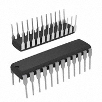


 工商网监
湘ICP备2023018690号
工商网监
湘ICP备2023018690号
