CAT3604A
4-Channel Regulated
Charge Pump White LED
Driver
Description
http://onsemi.com
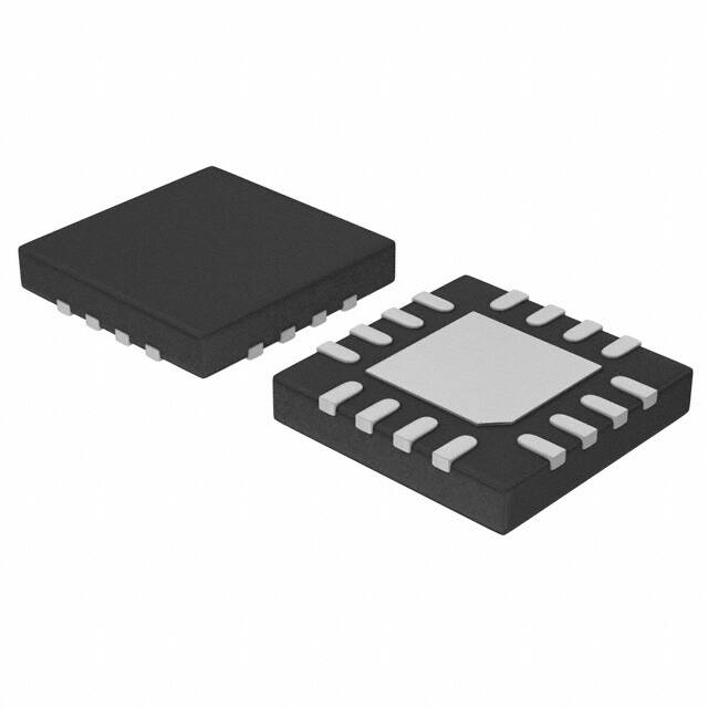
TQFN−16
HV4 SUFFIX
CASE 510AE
Applications
•
•
•
•
•
•
Color LCD and Keypad Backlighting
Cellular Phones
Handheld Devices
Digital Cameras
PDAs
Portable MP3 Players
© Semiconductor Components Industries, LLC, 2010
November, 2010 − Rev. 0
LED4
GND
CTR0
C2+
GND
CTR1
C2−
C1+
C1−
VIN
CTR2
RSET
Drives Individually up to 4 LEDs
Output Current up to 30 mA per LED
Compatible with Supply Voltage of 3 V to 5.5 V
Power Efficiency up to 93%
2 Modes of Operation 1x and 1.5x
LED On/Off by Control Lines
High−frequency Operation at 1 MHz
Low Value Ceramic Capacitors
“604” Compatible Pinout
Soft Start and Current Limiting
TQFN 16−pad Package, 4 x 4 mm, 0.8 mm Max Height
These Devices are Pb−Free, Halogen Free/BFR Free and are RoHS
Compliant
LED3
1
EN
Features
•
•
•
•
•
•
•
•
•
•
•
•
LED2
LED1
PIN CONNECTIONS (Note 1)
VOUT
The CAT3604A is a charge pump operating in either 1x (LDO)
mode or 1.5x fractional mode regulating current through each of the 4
LED pins. Operation at a fixed high frequency of 1 MHz typical
allows the use of very small value ceramic capacitors.
The CAT3604A drives white light-emitting diodes (LEDs)
connected in parallel and provides tightly matched regulated current to
achieve uniformity of brightness in LCD backlighting applications.
An external resistor RSET controls the output current level. LED
currents of up to 30 mA are supported over a range of input supply
voltages from 3 V to 5.5 V, making the device ideal for
battery-powered applications.
LED dimming can be accomplished by several methods including
using a DC voltage to set the RSET pin current, applying a PWM
signal on the Control signals, or adding a switched resistor in parallel
with RSET. The Enable input pin allows the device to be placed in
power-down mode with “zero” quiescent current.
The CAT3604A features short circuit and overcurrent limiting
protection. The device is available in a 16−pad TQFN package with a
max height of 0.8 mm.
(4 x 4 mm) (Top View)
MARKING DIAGRAMS
E364
E364 = CAT3604AHV4−T2
ORDERING INFORMATION
Device
Package
Shipping
CAT3604AHV4−T2
TQFN−16
(Note 2)
2,000/
Tape & Reel
1. The package exposed pad is electrically connected inside the package to GND and to pin 12.
2. Matte−Tin Plated Finish (RoHS−compliant).
1
Publication Order Number:
CAT3604A/D
�CAT3604A
1 μF
C1+
Battery +
−
VIN
3 V to 4.2 V
C1− C2+
VIN
CIN
EN
EN
1 μF
C2−
VOUT
CAT3604A
1 μF Control 0
CTR0
LED1
Control 1
CTR1
LED2
Control 2
CTR2
LED3
RSET
RSET
24 kW
VOUT
GND
LED4
Figure 1. Typical Application Circuit
Table 1. PIN DESCRIPTION
Pin #
Name
Function
1
EN
2
CTR0
Digital control input 0
3
CTR1
Digital control input 1
4
CTR2
Digital control input 2
5
RSET
The LED output current is set by the current sourced out of the RSET pin
6
VOUT
Charge pump output connected to the LED anodes
7
VIN
Supply voltage
8
C1+
Bucket capacitor 1 terminal
9
C1
Bucket capacitor 1 terminal
10
C2
Bucket capacitor 2 terminal
Enable input, active HIGH
11
C2+
Bucket capacitor 2 terminal
12
GND
Ground reference
13
LED4
LED 4 cathode terminal
14
LED3
LED 3 cathode terminal
15
LED2
LED 2 cathode terminal
16
LED1
LED 1 cathode terminal
Pad
GND Pad
Ground reference
http://onsemi.com
2
COUT
1 μF
20 mA
�CAT3604A
Table 2. ABSOLUTE MAXIMUM RATINGS
Parameter
Rating
Unit
VIN, VOUT, LEDx voltage
−0.3 to 7.0
V
EN, CTRx voltage
−0.3 to VIN
V
RSET voltage
−0.3 to VIN
V
RSET current
±1
mA
Ambient Temperature Range
−40 to +85
_C
Storage Temperature Range
−65 to +160
_C
300
_C
2,000
V
200
V
Lead Temperature
ESD Rating HBM (Human Body Model)
ESD Rating MM (Machine Model) (Note 3)
Stresses exceeding Maximum Ratings may damage the device. Maximum Ratings are stress ratings only. Functional operation above the
Recommended Operating Conditions is not implied. Extended exposure to stresses above the Recommended Operating Conditions may affect
device reliability.
3. Machine model is with 200 pF capacitor discharged directly into each pin.
Table 3. RECOMMENDED OPERATING CONDITIONS
Range
Unit
VIN
Parameter
3.0 to 5.5
V
Ambient Temperature Range
−40 to +85
_C
1 ±20% typical
mF
0 to 30
mA
Input/Output/Bucket Capacitors
ILED per LED pin
4. Typical application circuit with external components is shown on page 2.
Table 4. ELECTRICAL OPERATING CHARACTERISTICS
(Limits over recommended operating conditions unless specified otherwise. Typical values at TA = 25°C, VIN = 3.5 V, IRSET = 5 mA)
Symbol
IQ
Parameter
Quiescent Current
Conditions
Min
VEN = 0 V, Shutdown Mode
1x Mode, No Load
1.5x Mode, No Load
1.17
Typ
Max
Units
0.05
0.3
2.6
1
1
5
mA
mA
mA
1.2
1.23
V
VRSET
RSET Regulated Voltage
ILED
Programmed LED Current
IRSET = 5 mA
IRSET = 37 mA
IRSET = 78 mA
2.4
15.0
30.0
mA
ILED−ACC
LED Current Accuracy
0.5 mA ≤ ILED ≤ 3 mA
3 mA ≤ ILED ≤ 30 mA
±15
±5
%
ILED−DEV
LED Channel Matching
(ILED – ILEDAVG) / ILEDAVG
±3
%
ROUT
Output Resistance
(Open Loop)
1x Mode
1.5x Mode, IOUT = 100 mA
1.4
6.5
2.5
10
W
fOSC
Charge Pump Frequency
0.8
1.0
1.3
MHz
TDROPOUT
1x to 1.5x Mode Transition
Dropout Delay
0.4
0.6
0.9
ms
0.001
1
mA
IEN−CTR
Input Leakage Current
On Inputs EN, CTR0, 1 & 2
VEN−CTR
High Detect Threshold Low
On Inputs EN, CTR0, 1 & 2
0.4
0.8
1.3
V
ISC
Input Current Limit
VOUT = GND
30
45
60
mA
ILIM
Maximum Input Current
VOUT > 1 V
200
400
600
mA
http://onsemi.com
3
�CAT3604A
Block Diagram
1 μF
C1−
VIN −
3 V to 4.2 V
C1+ C2−
C2+
1x mode (LDO)
1.5x Charge Pump
VIN
Battery +
1 μF
VOUT
CIN
COUT
1 μF
1 μF
Mode Control
1 MHz
Oscillator
LED1
EN
LED2
LED3
1.2 V Ref
LED4
RSET
RSET
24 kW
CTR0
CTR1
CTR2
Current
Setting
4 Current
Sink Regulators
LED
Output
Select
GND
Figure 2. CAT3604A Functional Block Diagram
http://onsemi.com
4
20 mA
�CAT3604A
Basic Operation
At power-up, the CAT3604A starts operation in 1x mode.
If it is able to drive the programmed LED current, it
continues in 1x mode. If the battery voltage drops to a level
where the LED current cannot be met, the driver
automatically switches into 1.5x mode. The 1.5x charge
pump will boost the output voltage accordingly to achieve
the nominal LED current.
The operating mode is reinitialized each and every time
the chip is powered up or is taken out of shutdown mode (via
EN pin). The use of the control pins (CTR0, CTR1, CTR2)
does not reconfigure the mode of operation.
Table 5. RSET Resistor Selection
LED Current Setting
Table 6. LED Selection
The LED current is set by the external resistor RSET
connected between the RSET pin and ground. Table 5 lists
various LED currents and the associated RSET resistor value
for standard 1% precision surface mount resistors.
The digital control lines CTR0, CTR1 and CTR2 allow to
turn On or Off a combition of LEDs as shown in Table 6.
LED Current (mA)
RSET (kW)
1
649
2
287
5
102
10
49.9
15
32.4
20
23.7
30
15.4
Control Lines
CTR1
CTR0
LED4
LED3
LED2
LED1
0
0
0
–
–
–
ON
0
0
1
–
–
ON
–
0
1
0
–
ON
–
–
0
1
1
ON
−
–
–
1
0
0
–
–
ON
ON
1
0
1
–
ON
ON
ON
1
1
0
ON
ON
ON
ON
1
1
1
–
–
–
–
NOTE:
http://onsemi.com
5
LED Outputs
CTR2
1 = logic high (or VIN)
0 = logic low (or GND)
– = LED output OFF
�CAT3604A
TYPICAL CHARACTERISTICS
(VIN = 3.6 V, EN = VIN, CIN = COUT = 1 mF, RSET = 24 kW, TAMB = 25°C, unless otherwise specified.)
100
1x Mode
90
1.5x Mode
EFFICIENCY (%)
EFFICIENCY (%)
90
100
80
15 mA per LED
70
20 mA per LED
60
50
40
70
VIN = 3.2 V (1.5x Mode)
60
50
4.2
4.0
3.8
3.6
3.4
3.2
40
3.0
0
50
100
150
200
DISCHARGING BATTERY (V)
TOTAL LED CURRENT (mA)
Figure 3. Efficiency vs. Input Voltage
(4 LEDs)
Figure 4. Efficiency vs. Total LED Current
(4 LEDs)
16.0
24
22
1 LED at 20 mA
20
4 LEDs at 20 mA
4 LEDs at 15 mA
Vin = 4 V
LED CURRENT (mA)
LED CURRENT (mA)
VIN = 4 V (1x Mode)
80
18
16
4 LEDs at 15 mA
14
15.5
15.0
14.5
12
10
3.0
3.2
3.4
3.6
3.8
4.0
14.0
−50
4.2
25
50
75
100
TEMPERATURE (°C)
Figure 5. LED Current vs. Input Voltage
Figure 6. LED Current vs. Temperature
125
0.5
GROUND CURRENT (mA)
GROUND CURRENT (mA)
0
INPUT VOLTAGE (V)
0.5
0.4
0.3
0.2
4 LEDs Off
0.1
0
−25
3.0
3.2
3.4
3.6
3.8
4.0
0.4
0.3
0.2
0
−40
4.2
4 LEDs OFF
Rset = 500 kW
0.1
−20
0
20
40
60
80
INPUT VOLTAGE (V)
TEMPERATURE (°C)
Figure 7. Ground Current vs. Input Voltage
(1x Mode)
Figure 8. Ground Current vs. Temperature
(1x Mode)
http://onsemi.com
6
100
�CAT3604A
TYPICAL CHARACTERISTICS
5
100
4
80
SUPPLY CURRENT (mA)
GROUND CURRENT (mA)
(VIN = 3.6 V, EN = VIN, CIN = COUT = 1 mF, RSET = 24 kW, TAMB = 25°C, unless otherwise specified.)
3
2
VIN = 3.6 V
all LEDs open
1
1.5x Mode
1x Mode
60
40
20
4 LEDs at 15 mA
0
3.0
3.2
3.4
3.6
3.8
4.0
0
4.2
Figure 10. Supply Current vs. Input Voltage
4.2
1.10
CLOCK FREQUENCY (MHz)
CLOCK FREQUENCY (MHz)
4.0
Figure 9. Ground Current vs. Input Voltage
(1.5x Mode)
1.00
0.95
4 LEDs at 20 mA
3.0
3.2
3.4
3.6
3.8
4.0
1.05
1.00
VIN = 3.6 V
4 LEDs at 15 mA
0.95
0.90
−40
4.2
−20
0
40
20
60
80
INPUT VOLTAGE (V)
TEMPERATURE (°C)
Figure 11. Oscillator Frequency vs. Input
Voltage
Figure 12. Oscillator Frequency vs.
Temperature
100
10
OUTPUT RESISTANCE (W)
4
OUTPUT RESISTANCE (W)
3.8
3.6
INPUT VOLTAGE (V)
1.05
3
2
100 mA load
1
0
3.4
3.2
INPUT VOLTAGE (V)
1.10
0.90
3.0
3.0
3.2
3.4
3.6
3.8
4.0
8
100 mA load
6
4
2
4.2
25 mA load
3.0
3.2
3.4
3.6
3.8
4.0
4.2
INPUT VOLTAGE (V)
INPUT VOLTAGE (V)
Figure 13. Output Resistance vs. Input Voltage
(1x Mode)
Figure 14. Output Resistance vs. Input Voltage
(1.5x Mode)
http://onsemi.com
7
�CAT3604A
TYPICAL CHARACTERISTICS
(VIN = 3.6 V, EN = VIN, CIN = COUT = 1 mF, RSET = 24 kW, TAMB = 25°C, unless otherwise specified.)
VIN
50mV/
div
Input
Current
10mA/
div
AC coupled
VIN
50mV/div
AC coupled
AC coupled
Input
Current
10mA/div
AC coupled
VOUT
50mV/
div
VOUT
50mV/div
AC coupled
AC coupled
500 nsec/div
500 nsec/div
Figure 15. Switching Waveforms in 1.5x Mode
Figure 16. Operating Waveforms in 1x Mode
EN
2V/div
EN
2V/div
Input
Current
100mA/
div
Input
Current
100mA/div
VOUT
2V/div
VOUT
2V/div
500 msec/div
500 msec/div
Figure 17. Power Up 4 LEDs at 15 mA,
Vin = 3 V (1.5x Mode)
Figure 18. Power Up 4 LEDs at 15 mA,
Vin = 3.6 V (1x Mode)
LED CURRENT (mA)
100
Vin
3.6V to 4.9V
1V/div
LED Current
5mA/div
10
1
VOUT
2V/div
AC coupled
10
100
1000
200 msec/div
RSET (kW)
Figure 19. LED Current vs. RSET
Figure 20. Line Transient Response
in 1x Mode
http://onsemi.com
8
�CAT3604A
TYPICAL CHARACTERISTICS
(VIN = 3.6 V, EN = VIN, CIN = COUT = 1 mF, unless otherwise specified.)
OUTPUT VOLTAGE (V)
5
4
1x Mode
3
2
1
0
0
100
200
300
400
500
OUTPUT CURRENT (mA)
Figure 21. Foldback Current Limiting
Recommended Layout
A square copper area matches the QFN16 exposed pad
(GND) which is connected by a trace to the pin 12 pad
(GND). A large via (metalized hole) centered in the square
pad provides a low impedance connection to the ground
plane on the opposite side of the PCB and allows the heat
dissipated by the driver IC to spread out resulting in
excellent thermal performance.
When the driver is in the 1.5x charge pump mode, the
1 MHz switching frequency operation requires to minimize
trace length and impedance to ground on all 4 capacitors. A
ground plane should cover the area on the bottom side of the
PCB opposite to the IC and the bypass capacitors.
Capacitors Cin and Cout require short connection to ground
which can be done with multiple vias as shown on Figure 22.
0.76 mm
2.25 mm
Figure 22. PCB Layout
0.35 mm
Figure 23. Recommended QFN 16
Package Land Pattern
http://onsemi.com
9
4.41 mm
1.95 mm
2.25 mm
0.65 mm
�MECHANICAL CASE OUTLINE
PACKAGE DIMENSIONS
TQFN16, 4x4
CASE 510AE−01
ISSUE A
DATE 18 MAR 2009
A
D
DETAIL A
E2
E
PIN#1 ID
PIN#1 INDEX AREA
TOP VIEW
SIDE VIEW
SYMBOL
MIN
NOM
MAX
A
0.70
0.75
0.80
A1
0.00
0.02
0.05
A3
BOTTOM VIEW
e
b
0.20 REF
b
0.25
0.30
0.35
D
3.90
4.00
4.10
D2
2.00
−−−
2.25
E
3.90
4.00
4.10
E2
2.00
−−−
2.25
e
L
D2
A1
0.65 BSC
0.45
−−−
Notes:
(1) All dimensions are in millimeters.
(2) Complies with JEDEC MO-220.
DOCUMENT NUMBER:
DESCRIPTION:
98AON34374E
TQFN16, 4X4
0.65
L
DETAIL A
A
A1
A3
FRONT VIEW
Electronic versions are uncontrolled except when accessed directly from the Document Repository.
Printed versions are uncontrolled except when stamped “CONTROLLED COPY” in red.
PAGE 1 OF 1
ON Semiconductor and
are trademarks of Semiconductor Components Industries, LLC dba ON Semiconductor or its subsidiaries in the United States and/or other countries.
ON Semiconductor reserves the right to make changes without further notice to any products herein. ON Semiconductor makes no warranty, representation or guarantee regarding
the suitability of its products for any particular purpose, nor does ON Semiconductor assume any liability arising out of the application or use of any product or circuit, and specifically
disclaims any and all liability, including without limitation special, consequential or incidental damages. ON Semiconductor does not convey any license under its patent rights nor the
rights of others.
© Semiconductor Components Industries, LLC, 2019
www.onsemi.com
�ON Semiconductor and
are trademarks of Semiconductor Components Industries, LLC dba ON Semiconductor or its subsidiaries in the United States and/or other countries.
ON Semiconductor owns the rights to a number of patents, trademarks, copyrights, trade secrets, and other intellectual property. A listing of ON Semiconductor’s product/patent
coverage may be accessed at www.onsemi.com/site/pdf/Patent−Marking.pdf. ON Semiconductor reserves the right to make changes without further notice to any products herein.
ON Semiconductor makes no warranty, representation or guarantee regarding the suitability of its products for any particular purpose, nor does ON Semiconductor assume any liability
arising out of the application or use of any product or circuit, and specifically disclaims any and all liability, including without limitation special, consequential or incidental damages.
Buyer is responsible for its products and applications using ON Semiconductor products, including compliance with all laws, regulations and safety requirements or standards,
regardless of any support or applications information provided by ON Semiconductor. “Typical” parameters which may be provided in ON Semiconductor data sheets and/or
specifications can and do vary in different applications and actual performance may vary over time. All operating parameters, including “Typicals” must be validated for each customer
application by customer’s technical experts. ON Semiconductor does not convey any license under its patent rights nor the rights of others. ON Semiconductor products are not
designed, intended, or authorized for use as a critical component in life support systems or any FDA Class 3 medical devices or medical devices with a same or similar classification
in a foreign jurisdiction or any devices intended for implantation in the human body. Should Buyer purchase or use ON Semiconductor products for any such unintended or unauthorized
application, Buyer shall indemnify and hold ON Semiconductor and its officers, employees, subsidiaries, affiliates, and distributors harmless against all claims, costs, damages, and
expenses, and reasonable attorney fees arising out of, directly or indirectly, any claim of personal injury or death associated with such unintended or unauthorized use, even if such
claim alleges that ON Semiconductor was negligent regarding the design or manufacture of the part. ON Semiconductor is an Equal Opportunity/Affirmative Action Employer. This
literature is subject to all applicable copyright laws and is not for resale in any manner.
PUBLICATION ORDERING INFORMATION
LITERATURE FULFILLMENT:
Email Requests to: orderlit@onsemi.com
ON Semiconductor Website: www.onsemi.com
◊
TECHNICAL SUPPORT
North American Technical Support:
Voice Mail: 1 800−282−9855 Toll Free USA/Canada
Phone: 011 421 33 790 2910
www.onsemi.com
1
Europe, Middle East and Africa Technical Support:
Phone: 00421 33 790 2910
For additional information, please contact your local Sales Representative
�