CM1621
LCD and Camera EMI Filter
Array with ESD Protection
Features
• Six Channels of EMI Filtering with Integrated ESD Protection
• Pi−Style EMI Filters in a Capacitor−Resistor−Capacitor (C−R−C)
http://onsemi.com
Network
• ±15 kV ESD Protection on Each Channel
•
•
•
•
12
(IEC 61000−4−2 Level 4, Contact Discharge)
±30 kV ESD Protection on Each Channel (HBM)
Greater than 40 dB Attenuation (Typical) at 1 GHz
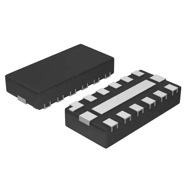
uDFN Package with 0.40 mm Lead Pitch:
• 12−Lead: 2.50 mm x 1.20 mm x 0.50 mm
These Devices are Pb−Free and are RoHS Compliant
1
UDFN12
DE SUFFIX
CASE 517AE
MARKING DIAGRAM
Applications
P21 M
G
• LCD and Camera Data Lines in Mobile Handsets
• I/O Port Protection for Mobile Handsets, Notebook Computers,
•
•
•
PDAs, etc.
EMI Filtering for Data Ports in Cell Phones, PDAs or Notebook
Computers
Wireless Handsets
Handheld PCs/PDAs
BLOCK DIAGRAM
100 W
FILTER+ESDn*
R
C
17 pF
FILTER+ESDn*
17 pF
1
P21
M
G
= CM1621−06DE
= Month Code
= Pb−Free Package
ORDERING INFORMATION
Device
Package
Shipping†
CM1621−06DE
uDFN−12
(Pb−Free)
3000/Tape & Reel
†For information on tape and reel specifications,
including part orientation and tape sizes, please
refer to our Tape and Reel Packaging Specification
Brochure, BRD8011/D.
C
GND
1 of 6 EMI / RFI + ESD Channels
*See Package/Pinout Diagrams for expanded pin information.
© Semiconductor Components Industries, LLC, 2011
April, 2011 − Rev. 3
1
Publication Order Number:
CM1621/D
�CM1621
PACKAGE / PINOUT DIAGRAMS
Pin 1
Marking
Top View
(Pins Down View)
Bottom View
(Pins Up View)
14 13 12 11 10 9
1 2 3 4 5 6
P21
GND
PAD
1 2 3 4 5 6
14 13 12 11 10 9
12−Lead UDFN Package
Table 1. PIN DESCRIPTIONS
Device Pin(s)
Name
1
FILTER1
2
FILTER2
3
Description
Device Pin(s)
Name
Description
Filter + ESD Channel 1
12
FILTER1
Filter + ESD Channel 1
Filter + ESD Channel 2
11
FILTER2
Filter + ESD Channel 2
FILTER3
Filter + ESD Channel 3
10
FILTER3
Filter + ESD Channel 3
4
FILTER4
Filter + ESD Channel 4
9
FILTER4
Filter + ESD Channel 4
5
FILTER5
Filter + ESD Channel 5
8
FILTER5
Filter + ESD Channel 5
6
FILTER6
Filter + ESD Channel 6
7
FILTER6
Filter + ESD Channel 6
GND PAD
GND
Device Ground
SPECIFICATIONS
Table 2. ABSOLUTE MAXIMUM RATINGS
Parameter
Rating
Storage Temperature Range
Units
−65 to +150
°C
DC Power per Resistor
100
mW
DC Package Power Rating
500
mW
Stresses exceeding Maximum Ratings may damage the device. Maximum Ratings are stress ratings only. Functional operation above the
Recommended Operating Conditions is not implied. Extended exposure to stresses above the Recommended Operating Conditions may affect
device reliability.
Table 3. STANDARD OPERATING CONDITIONS
Parameter
Operating Temperature Range
http://onsemi.com
2
Rating
Units
−40 to +85
°C
�CM1621
Table 4. ELECTRICAL OPERATING CHARACTERISTICS (Note 1)
Symbol
R
CTOTAL
Parameter
Conditions
Resistance
Min
Typ
Max
Units
85
100
115
W
27
34
41
pF
Total Channel Capacitance
At 2.5 VDC Reverse Bias,
1 MHz, 30 mVAC
Capacitance C
At 2.5 VDC Reverse Bias,
1 MHz, 30 mVAC
17
pF
Standoff Voltage
IDIODE = 10 mA
6.0
V
ILEAK
Diode Leakage Current (reverse bias)
VDIODE = +3.3 V
VSIG
Signal Clamp Voltage
ILOAD = 1.0 mA
VESD
In−system ESD Withstand Voltage
a) Human Body Model (HBM), MIL−STD−883,
Method 3015
b) Contact Discharge per IEC 61000−4−2 Level 4
(Note 2)
C
VDIODE
RDYN
fC
A1GHz
A800MHz
− 3 GHz
6.0
7.0
100
nA
8.0
V
kV
±30
±15
Dynamic Resistance
Positive
Negative
W
2.3
0.9
Cut−off Frequency
ZSOURCE = 50 W, ZLOAD = 50 W
Channel R = 100 W,
Channel C = 15 pF
90
Absolute Attenuation at 1 GHz from 0 dB Level
ZSOURCE = 50 W, ZLOAD = 50 W,
DC Bias = 0 V; (Notes 1 and 3)
−40
dB
Absolute Attenuation at 800 MHz to 3 Ghz
from 0 dB Level
ZSOURCE = 50 W, ZLOAD = 50 W,
DC Bias = 0 V; (Notes 1 and 3)
−35
dB
1. TA = 25°C unless otherwise specified.
2. ESD applied to input and output pins with respect to GND, one at a time.
3. Attenuation / RF curves characterized by a network analyzer using microprobes.
http://onsemi.com
3
135
(Note 3)
MHz
�CM1621
PERFORMANCE INFORMATION
Typical Filter Performance (TA = 255C, DC Bias = 0 V, 50 W Environment)
Figure 1. Insertion Loss vs. Frequency (FILTER1 Input to GND, CM1621−06DE)
Typical Diode Capacitance vs. Input Voltage
Figure 2. Insertion Loss vs. Frequency (FILTER2 Input to GND, CM1621−06DE)
Typical Diode Capacitance vs. Input Voltage
http://onsemi.com
4
�CM1621
PERFORMANCE INFORMATION (Cont’d)
Typical Filter Performance (TA = 255C, DC Bias = 0 V, 50 W Environment)
Figure 3. Insertion Loss vs. Frequency (FILTER3 Input to GND, CM1621−06DE)
Typical Diode Capacitance vs. Input Voltage
Figure 4. Insertion Loss vs. Frequency (FILTER4 Input to GND, CM1621−06DE)
Typical Diode Capacitance vs. Input Voltage
http://onsemi.com
5
�CM1621
PERFORMANCE INFORMATION (Cont’d)
Typical Filter Performance (TA = 255C, DC Bias = 0 V, 50 W Environment)
Figure 5. Insertion Loss vs. Frequency (FILTER5 Input to GND, CM1621−06DE)
Typical Diode Capacitance vs. Input Voltage
Figure 6. Insertion Loss vs. Frequency (FILTER6 Input to GND, CM1621−06DE)
Typical Diode Capacitance vs. Input Voltage
http://onsemi.com
6
�CM1621
Capacitance (Normalized)
PERFORMANCE INFORMATION (Cont’d)
DC Voltage
Figure 7. Filter Capacitance vs. Input Voltage
(normalized to capacitance at 2.5 VDC and 255C)
http://onsemi.com
7
�MECHANICAL CASE OUTLINE
PACKAGE DIMENSIONS
UDFN12 2.5x1.2, 0.4P
CASE 517AE
ISSUE C
12
1
DATE 23 OCT 2012
SCALE 4:1
0.15 C
PIN ONE
REFERENCE
2X
A3
A
B
D
2X
ÉÉÉ
ÉÉÉ
NOTES:
1. DIMENSIONING AND TOLERANCING PER
ASME Y14.5M, 1994.
2. CONTROLLING DIMENSION: MILLIMETERS.
3. DIMENSION b APPLIES TO PLATED TERMINAL
AND IS MEASURED BETWEEN 0.25 AND
0.30 mm FROM TERMINAL.
4. COPLANARITY APPLIES TO THE EXPOSED
PAD AS WELL AS THE TERMINALS.
ÇÇ
ÉÉ
E
A1
DETAIL B
OPTIONAL
CONSTRUCTION
0.15 C
TOP VIEW
(A3)
DETAIL B
A
0.10 C
12X
SEATING
PLANE
0.08 C
SIDE VIEW
C
A1
L1
D2
DETAIL A
12X
L
1
e
(0.10)
E2
MILLIMETERS
MIN
NOM MAX
0.45
0.50
0.55
0.00
0.03
0.05
0.127 REF
0.15
0.20
0.25
2.50 BSC
1.70
1.80
1.90
1.20 BSC
0.20
0.30
0.40
0.40 BSC
0.20 TYP
0.20
0.25
0.30
−−−
−−−
0.10
GENERIC
MARKING DIAGRAM*
10X
6
L
DIM
A
A1
A3
b
D
D2
E
E2
e
K
L
L1
XXXM
G
DETAIL A
OPTIONAL
CONSTRUCTION
12X
K
12
7
12X
b
XXX
M
G
0.10 C A B
BOTTOM VIEW
0.05 C
1
NOTE 3
= Specific Device Code
= Month Code
= Pb−Free Package
*This information is generic. Please refer
to device data sheet for actual part
marking.
Pb−Free indicator, “G” or microdot “ G”,
may or may not be present.
SOLDERING FOOTPRINT*
1.50
0.35
0.40
1.90
11X
0.25
0.40 PITCH
12 X
0.45
DIMENSIONS: MILLIMETERS
*For additional information on our Pb−Free strategy and soldering
details, please download the ON Semiconductor Soldering and
Mounting Techniques Reference Manual, SOLDERRM/D.
DOCUMENT NUMBER:
DESCRIPTION:
98AON22155D
UDFN12 2.5X1.2, 0.4P
Electronic versions are uncontrolled except when accessed directly from the Document Repository.
Printed versions are uncontrolled except when stamped “CONTROLLED COPY” in red.
PAGE 1 OF 1
ON Semiconductor and
are trademarks of Semiconductor Components Industries, LLC dba ON Semiconductor or its subsidiaries in the United States and/or other countries.
ON Semiconductor reserves the right to make changes without further notice to any products herein. ON Semiconductor makes no warranty, representation or guarantee regarding
the suitability of its products for any particular purpose, nor does ON Semiconductor assume any liability arising out of the application or use of any product or circuit, and specifically
disclaims any and all liability, including without limitation special, consequential or incidental damages. ON Semiconductor does not convey any license under its patent rights nor the
rights of others.
© Semiconductor Components Industries, LLC, 2019
www.onsemi.com
�onsemi,
, and other names, marks, and brands are registered and/or common law trademarks of Semiconductor Components Industries, LLC dba “onsemi” or its affiliates
and/or subsidiaries in the United States and/or other countries. onsemi owns the rights to a number of patents, trademarks, copyrights, trade secrets, and other intellectual property.
A listing of onsemi’s product/patent coverage may be accessed at www.onsemi.com/site/pdf/Patent−Marking.pdf. onsemi reserves the right to make changes at any time to any
products or information herein, without notice. The information herein is provided “as−is” and onsemi makes no warranty, representation or guarantee regarding the accuracy of the
information, product features, availability, functionality, or suitability of its products for any particular purpose, nor does onsemi assume any liability arising out of the application or use
of any product or circuit, and specifically disclaims any and all liability, including without limitation special, consequential or incidental damages. Buyer is responsible for its products
and applications using onsemi products, including compliance with all laws, regulations and safety requirements or standards, regardless of any support or applications information
provided by onsemi. “Typical” parameters which may be provided in onsemi data sheets and/or specifications can and do vary in different applications and actual performance may
vary over time. All operating parameters, including “Typicals” must be validated for each customer application by customer’s technical experts. onsemi does not convey any license
under any of its intellectual property rights nor the rights of others. onsemi products are not designed, intended, or authorized for use as a critical component in life support systems
or any FDA Class 3 medical devices or medical devices with a same or similar classification in a foreign jurisdiction or any devices intended for implantation in the human body. Should
Buyer purchase or use onsemi products for any such unintended or unauthorized application, Buyer shall indemnify and hold onsemi and its officers, employees, subsidiaries, affiliates,
and distributors harmless against all claims, costs, damages, and expenses, and reasonable attorney fees arising out of, directly or indirectly, any claim of personal injury or death
associated with such unintended or unauthorized use, even if such claim alleges that onsemi was negligent regarding the design or manufacture of the part. onsemi is an Equal
Opportunity/Affirmative Action Employer. This literature is subject to all applicable copyright laws and is not for resale in any manner.
PUBLICATION ORDERING INFORMATION
LITERATURE FULFILLMENT:
Email Requests to: orderlit@onsemi.com
onsemi Website: www.onsemi.com
◊
TECHNICAL SUPPORT
North American Technical Support:
Voice Mail: 1 800−282−9855 Toll Free USA/Canada
Phone: 011 421 33 790 2910
Europe, Middle East and Africa Technical Support:
Phone: 00421 33 790 2910
For additional information, please contact your local Sales Representative
�