ON Semiconductor
Is Now
To learn more about onsemi™, please visit our website at
www.onsemi.com
onsemi and and other names, marks, and brands are registered and/or common law trademarks of Semiconductor Components Industries, LLC dba “onsemi” or its affiliates and/or
subsidiaries in the United States and/or other countries. onsemi owns the rights to a number of patents, trademarks, copyrights, trade secrets, and other intellectual property. A listing of onsemi
product/patent coverage may be accessed at www.onsemi.com/site/pdf/Patent-Marking.pdf. onsemi reserves the right to make changes at any time to any products or information herein, without
notice. The information herein is provided “as-is” and onsemi makes no warranty, representation or guarantee regarding the accuracy of the information, product features, availability, functionality,
or suitability of its products for any particular purpose, nor does onsemi assume any liability arising out of the application or use of any product or circuit, and specifically disclaims any and all
liability, including without limitation special, consequential or incidental damages. Buyer is responsible for its products and applications using onsemi products, including compliance with all laws,
regulations and safety requirements or standards, regardless of any support or applications information provided by onsemi. “Typical” parameters which may be provided in onsemi data sheets and/
or specifications can and do vary in different applications and actual performance may vary over time. All operating parameters, including “Typicals” must be validated for each customer application
by customer’s technical experts. onsemi does not convey any license under any of its intellectual property rights nor the rights of others. onsemi products are not designed, intended, or authorized
for use as a critical component in life support systems or any FDA Class 3 medical devices or medical devices with a same or similar classification in a foreign jurisdiction or any devices intended for
implantation in the human body. Should Buyer purchase or use onsemi products for any such unintended or unauthorized application, Buyer shall indemnify and hold onsemi and its officers, employees,
subsidiaries, affiliates, and distributors harmless against all claims, costs, damages, and expenses, and reasonable attorney fees arising out of, directly or indirectly, any claim of personal injury or death
associated with such unintended or unauthorized use, even if such claim alleges that onsemi was negligent regarding the design or manufacture of the part. onsemi is an Equal Opportunity/Affirmative
Action Employer. This literature is subject to all applicable copyright laws and is not for resale in any manner. Other names and brands may be claimed as the property of others.
�CS8147
10 V/5.0 V Low Dropout
Dual Regulator with ENABLE
The CS8147 is a 10 V/5.0 V dual output linear regulator. The 10V
±5.0% output sources 500 mA and the 5.0 V ±3% output sources 70
mA. The secondary output is inherently stable and does not require an
external capacitor.
The on board ENABLE function controls the regulator’s two
outputs. When ENABLE is high, the regulator is placed in SLEEP
mode. Both outputs are disabled and the regulator draws only 70 µA of
quiescent current.
The regulator is protected against overvoltage conditions. Both
outputs are protected against short circuit and thermal runaway
conditions.
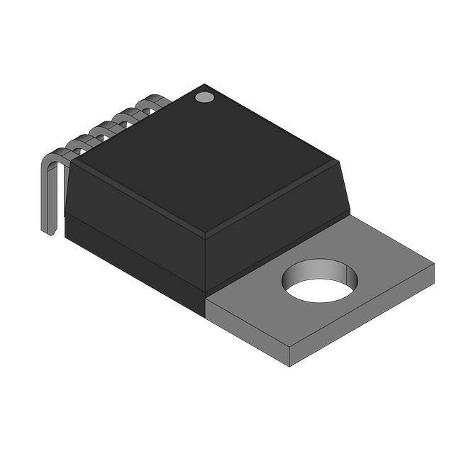
The CS8147 is packaged in a 5 lead TO–220 with copper tab. The
copper tab can be connected to a heat sink if necessary.
http://onsemi.com
TO–220
FIVE LEAD
T SUFFIX
CASE 314D
1
5
TO–220
FIVE LEAD
TVA SUFFIX
CASE 314K
1
Features
• Two Regulated Outputs
– 10 V ±5.0%; 500 mA
– 5.0 V ±3.0%; 70 mA
• 70 µA SLEEP Mode Current
• Inherently Stable Secondary Output (No Output Capacitor Required)
• Fault Protection
– Overvoltage Shutdown
– Reverse Battery
– 60 V Peak Transient
– –50 V Reverse Transient
– Short Circuit
– Thermal Shutdown
• CMOS Compatible ENABLE Input with Low (IOUT(max)) Input
Current
1
TO–220
FIVE LEAD
THA SUFFIX
CASE 314A
5
PIN CONNECTIONS AND
MARKING DIAGRAM
CS8147
AWLYWW
Tab = GND
Pin 1. ENABLE
2. VIN
3. GND
4. VOUT1 (10 V)
5. VOUT2 (5.0 V)
1
A
WL, L
YY, Y
WW, W
= Assembly Location
= Wafer Lot
= Year
= Work Week
ORDERING INFORMATION
Device
Package
Shipping
CS8147YT5
TO–220*
STRAIGHT
50 Units/Rail
CS8147YTVA5
TO–220*
VERTICAL
50 Units/Rail
CS8147YTHA5
TO–220*
HORIZONTAL
50 Units/Rail
*Five lead.
Semiconductor Components Industries, LLC, 2001
January, 2001 – Rev. 6
1
Publication Order Number:
CS8147/D
�CS8147
Primary Output
VOUT1
VIN
Overvoltage
Shutdown
Anti–saturation
and
Current Limit
ENABLE
–
+
+
–
Pre–Regulator
Secondary Output
Bandgap
Reference
–
+
VOUT2
GND
Thermal
Shutdown
Current Limit
Figure 1. Block Diagram
ABSOLUTE MAXIMUM RATINGS*
Rating
Value
Unit
–18 to 26
60
–50
V
V
V
2.0
kV
–0.3 to 10
V
Internally Limited
–
Junction Temperature Range
–40 to +150
°C
Storage Temperature Range
–65 to +150
°C
260 peak
°C
Input Voltage:
DC
Positive Peak Transient Voltage (Note 1.)
Negative Peak Transient Voltage
ESD (Human Body Model)
ENABLE Input
Internal Power Dissipation
Lead Temperature Soldering:
Wave Solder (through hole styles only) (Note 2.)
1. 46 V Load Dump @ VIN = 14 V
2. 10 second maximum.
*The maximum package power dissipation must be observed.
http://onsemi.com
2
�CS8147
ELECTRICAL CHARACTERISTICS for VOUT: (VIN = 14 V, IOUT1 = IOUT2 = 5.0 mA, –40°C < TJ < 150°C,
–40°C ≤ TA ≤ 125°C, ENABLE = LOW; unless otherwise specified.)
Test Conditions
Characteristic
Min
Typ
Max
Unit
9.50
10.00
10.5
V
Primary Output (VOUT1)
Output Voltage
13 V ≤ VIN ≤ 26 V, IOUT1 ≤ 500 mA
Dropout Voltage
IOUT1 = 500 mA
–
0.5
0.7
V
Line Regulation
11 V ≤ VIN ≤ 18 V, IOUT1 = 250 mA
–
45
90
mV
Load Regulation
5.0 mA ≤ IOUT1 ≤ 500 mA
–
15
75
mV
Quiescent Current
IOUT1 ≤ 1.0 mA, No Load on VOUT2, VIN = 18 V
IOUT1 = 500 mA, No Load on VOUT2, VIN = 11 V
–
–
3.0
60
7.0
120
mA
mA
Quiescent Current
ENABLE = HIGH, VOUT1, VOUT2 = OFF
–
70
200
µA
Current Limit
–
0.55
0.80
–
A
Long Term Stability
–
–
50
–
mV/khr
32
36
40
V
4.85
5.00
5.15
V
Overvoltage Shutdown
VOUT1 and VOUT2
Secondary Output (VOUT2)
Output Voltage
6.0 V ≤ VIN ≤ 26 V, 1.0 mA ≤ IOUT2 ≤ 70 mA
Dropout Voltage
IOUT2 ≤ 70 mA
–
1.5
2.5
V
Line Regulation
11 ≤ VIN ≤ 18 V, IOUT = 70 µA
–
4.0
50
mV
Load Regulation
1.0 mA ≤ IOUT2 ≤ 70 mA, VIN = 14 V
–
10
50
mV
–
150
–
mA
Current Limit
–
ENABLE Function (ENABLE)
Input ENABLE Threshold
VOUT2(ON)
VOUT1(OFF)
–
0.8
1.40
1.40
2.50
–
V
V
Input ENABLE Current
Input Voltage Range 0 to 5.0 V
–10
–
10
µA
PACKAGE PIN DESCRIPTION
PACKAGE LEAD #
5 Lead TO–220
LEAD SYMBOL
1
ENABLE
2
VIN
3
GND
4
VOUT1
Regulated output 10 V, 500 mA (typ).
5
VOUT2
Secondary output 5.0 V, 70 mA (typ).
FUNCTION
CMOS compatible input lead; switches VOUT1 and VOUT2 on
and off. When ENABLE is low, VOUT1 and VOUT2 are active.
Supply voltage, usually direct from battery.
Ground connection.
http://onsemi.com
3
�CS8147
2.00
600
550
500
450
400
125°C
350
25°C
300
250
–40°C
200
150
100
1.60
25°C
1.40
1.20
125°C
1.00
0.80
0.60
VIN = 6.00 V
0.40
0.20
50
0
0
0
0
50 100 150 200 250 300 350 400 450 500 550 600
20
30
40
50
60
70
80
Output Current (mA), VOUT2 (5.0 V)
Figure 2. Dropout Voltage vs.
Output Current (VOUT1)
Figure 3. Dropout Voltage vs.
Output Current (VOUT2)
90 100
7.0
90
25°C
125°C
70
60
–40°C
50
6.0
Quiescent Current (mA)
80
VIN = 14 V
40
30
20
5.0
–40°C
4.0
25°C
3.0
125°C
2.0
1.0
10
VIN = 14 V
0
0
0
0
50 100 150 200 250 300 350 400 450 500 550 600
20
30
40
50
60
70
80
Output Current (mA), VOUT2 (5.0 V)
Figure 4. Quiescent Current vs.
Output Current (VOUT1)
Figure 5. Quiescent Current vs.
Output Current (VOUT2)
90 100
120
110
100
Line Regulation (mV)
5.01
5.00
4.99
125°C
VIN = 11 V – 26 V
90
80
25°C
70
–40°C
60
50
40
30
20
10
0
4.98
–50
10
Output Current (mA)
5.02
VOUT (Volts)
10
Output Current (mA)
100
Quiescent Current (mA)
–40°C
1.80
Dropout Voltage (V), VOUT2
Dropout Voltage (mV), VOUT1
TYPICAL PERFORMANCE CHARACTERISTICS
–30
–10
10
30
50
70
90
110
130
0
50 100 150 200 250 300 350 400 450 500 550 600
Output Current (mA), VOUT1 (10 V)
Temp (C°)
PART1 VIN = 14 V, No Load
Figure 7. Line Regulation vs.
Output Current (VOUT1)
Figure 6. VOUT2 vs. Temperature
http://onsemi.com
4
�CS8147
30
10
26
9.0
125°C
VIN = 14 V
18
8.0
Load Regulation (mV)
Load Regulation (mV)
22
25°C
14
–40°C
10
6
2
125°C
VIN = 14 V
7.0
6.0
25°C
5.0
4.0
–40°C
3.0
–2
2.0
–6
1.0
–10
0
0
0
50 100 150 200 250 300 350 400 450 500 550 600
10
20
30
40
50
60
70
80
Output Current (mA), VOUT1 (10 V)
Output Current (mA), VOUT2 (5.0 V)
Figure 8. Load Regulation vs.
Output Current (VOUT1)
Figure 9. Load Regulation vs.
Output Current (VOUT2)
90 100
350
–40°C
100.0
300
V10 = 500 mA Load
V5 = 70 mA Load
IENABLE (µA)
250
ICQ (mA)
20.00
/div
0
25°C
200
150
125°C
100
50
0
–100.0
–1.000
0
0
9.000
2
3
4
5
6
7
8
9 10 11 12 13 14 15
VIN (V)
Figure 10. ENABLE Input Current vs.
Input Voltage
Figure 11. Quiescent Current (ICQ) vs.
VIN Overtemperature
300
10.025
VOUT1 = 500 mA Load
VIN = 14 V
IO = 30 mA
10.020
VOUT2 = 100 mA Load
250
10.015
10.010
150
VOUT (V)
200
ICQ (mA)
1
VENABLE 1.000/div (V)
VOUT1 = 500 mA Load
VOUT2 = No Load
100
10.005
10.000
9.995
9.990
9.985
50
VOUT1 = No Load
9.980
VOUT2 = No Load
0
9.975
0
1
2
3
4
5
6
7
8
9 10 11 12 13 14 15
–50 –30 –10
10
30
50
70
90
110 130 150
VIN (V)
TEMP (°C)
Figure 12. Quiescent Current (ICQ) vs.
VIN Over RLOAD
Figure 13. VOUT1 vs. Temperature
http://onsemi.com
5
�CS8147
DEFINITION OF TERMS
Load Regulation – The change in output voltage for a
change in load current at constant chip temperature.
Long Term Stability – Output voltage stability under
accelerated life–test conditions after 1000 hours with
maximum rated voltage and junction temperature.
Output Noise Voltage – The rms AC voltage at the
output, with constant load and no input ripple, measured
over a specified frequency range.
Quiescent Current – The part of the positive input
current that does not contribute to the positive load current.
The regulator ground lead current.
Ripple Rejection – The ratio of the peak–to–peak input
ripple voltage to the peak–to–peak output ripple voltage.
Temperature Stability of VOUT – The percentage
change in output voltage for a thermal variation from room
temperature to either temperature extreme.
Dropout Voltage – The input–output voltage differential
at which the circuit ceases to regulate against further
reduction in input voltage. Measured when the output
voltage has dropped 100 mV from the nominal value
obtained at 14 V input, dropout voltage is dependent upon
load current and junction temperature.
Current Limit – Peak current that can be delivered to the
output.
Input Voltage – The DC voltage applied to the input
terminals with respect to ground.
Input Output Differential – The voltage difference
between the unregulated input voltage and the regulated
output voltage for which the regulator will operate.
Line Regulation – The change in output voltage for a
change in the input voltage. The measurement is made under
conditions of low dissipation or by using pulse techniques
such that the average chip temperature is not significantly
affected.
60 V
VIN
14 V
ENABLE
2.0 V
0.8 V
31 V
26 V
14V
5.0 V
10 V
10 V
10 V
10 V
5.0 V
VOUT1
0V
0V
5.0 V
VOUT2
5.0 V
5.0 V
3.0 V
5.0 V
Load
Dump
Line
Noise, Etc.
Low VIN
0V
5.0 V
0V
0V
0V
Turn
On
10 V
0V
VOUT
Short
Circuit
Thermal
Shutdown
Figure 14. Typical Circuit Waveform
C1 *
0.1 µF
ENABLE
10V
VOUT1
CS8147
Control
VIN
C2**
10 µF
5.0V
VOUT2
GND
* C1 is required if the regulator is located away from the power source filter.
** C2 is required for stability.
Figure 15. Test & Applications Circuit
http://onsemi.com
6
Tuner IC
0V
Turn
Off
�CS8147
APPLICATION NOTES
This point represents the worst case input voltage
conditions.
Step 5: If the capacitor is adequate, repeat steps 3 and 4 with
the next smaller valued capacitor. A smaller capacitor will
usually cost less and occupy less board space. If the output
oscillates within the range of expected operating conditions,
repeat steps 3 and 4 with the next larger standard capacitor
value.
Step 6: Test the load transient response by switching in
various loads at several frequencies to simulate its real
working environment. Vary the ESR to reduce ringing.
Step 7: Raise the temperature to the highest specified
operating temperature. Vary the load current as instructed in
step 5 to test for any oscillations.
Once the minimum capacitor value with the maximum
ESR is found for each output, a safety factor should be added
to allow for the tolerance of the capacitor and any variations
in regulator performance. Most good quality aluminum
electrolytic capacitors have a tolerance of ±20% so the
minimum value found should be increased by at least 50%
to allow for this tolerance plus the variation which will occur
at low temperatures. The ESR of the capacitors should be
less than 50% of the maximum allowable ESR found in step
3 above.
Since both outputs are controlled by the same ENABLE,
the CS8147 is ideal for applications where a sleep mode is
required. Using the CS8147, a section of circuitry such as a
display and nonessential 5.0 V circuits can be shut down
under microprocessor control to conserve energy.
The test applications circuit diagram shows an automotive
radio application where the display is powered by 10 V from
VOUT1 and the Tuner IC is powered by 5.0 V from VOUT2.
Neither output is required unless both the ignition and the
Radio On/OFF switch are on.
Stability Considerations
The secondary output VOUT2 is inherently stable and does
not require a compensation capacitor. However a
compensation capacitor connected between VOUT1 and
ground is required for stability in most applications.
The output or compensation capacitor helps determine
three main characteristics of a linear regulator: start–up
delay, load transient response and loop stability.
The capacitor value and type should be based on cost,
availability, size and temperature constraints. A tantalum or
aluminum electrolytic capacitor is best, since a film or
ceramic capacitor with almost zero ESR can cause
instability. The aluminum electrolytic capacitor is the least
expensive solution, but, if the circuit operates at low
temperatures (–25°C to –40°C), both the value and ESR of
the capacitor will vary considerably. The capacitor
manufacturers data sheet usually provides this information.
The value for the output capacitor C2 shown in the test and
applications circuit should work for most applications,
however it is not necessarily the optimized solution.
To determine acceptable value for C2 for a particular
application, start with a tantalum capacitor of the
recommended value and work towards a less expensive
alternative part.
Step 1: Place the completed circuit with a tantalum
capacitor of the recommended value in an environmental
chamber at the lowest specified operating temperature and
monitor the outputs with an oscilloscope. A decade box
connected in series with the capacitor will simulate the
higher ESR of an aluminum capacitor. Leave the decade box
outside the chamber, the small resistance added by the
longer leads is negligible.
Step 2: With the input voltage at its maximum value,
increase the load current slowly from zero to full load while
observing the output for any oscillations. If no oscillations
are observed, the capacitor is large enough to ensure a stable
design under steady state conditions.
Step 3: Increase the ESR of the capacitor from zero using the
decade box and vary the load current until oscillations
appear. Record the values of load current and ESR that cause
the greatest oscillation. This represents the worst case load
conditions for the regulator at low temperature.
Step 4: Maintain the worst case load conditions set in step
3 and vary the input voltage until the oscillations increase.
Calculating Power Dissipation in a
Dual Output Linear Regulator
The maximum power dissipation for a dual output
regulator (Figure 16) is
PD(max) � �VIN(max) � VOUT1(min)�IOUT1(max) �
�VIN(max) � VOUT2(min)�IOUT2(max) � VIN(max)IQ (1)
where:
VIN(max) is the maximum input voltage,
VOUT1(min) is the minimum output voltage from VOUT1,
VOUT2(min) is the minimum output voltage from VOUT2,
IOUT1(max) is the maximum output current, for the
application,
IOUT2(max) is the maximum output current, for the
application, and
IQ is the quiescent current the regulator consumes at
IOUT(max).
Once the value of PD(max) is known, the maximum
permissible value of RΘJA can be calculated:
R�JA �
150°C � TA
PD
(2)
The value of RΘJA can be compared with those in the
package section of the data sheet. Those packages with
RΘJA’s less than the calculated value in equation 2 will keep
the die temperature below 150°C.
In some cases, none of the packages will be sufficient to
dissipate the heat generated by the IC, and an external
heatsink will be required.
http://onsemi.com
7
�CS8147
IIN
VIN
Smart
Regulator
Control
Features
Each material in the heat flow path between the IC and the
outside environment will have a thermal resistance. Like
series electrical resistances, these resistances are summed to
determine the value of RΘJA:
IOUT1
VOUT1
IOUT2
R�JA � R�JC � R�CS � R�SA
VOUT2
(3)
where:
RΘJC = the junction–to–case thermal resistance,
RΘCS = the case–to–heatsink thermal resistance, and
RΘSA = the heatsink–to–ambient thermal resistance.
IQ
RΘJC appears in the package section of the data sheet. Like
RΘJA, it too is a function of package type. RΘCS and RΘSA
are functions of the package type, heatsink and the interface
between them. These values appear in heat sink data sheets
of heat sink manufacturers.
Figure 16. Dual Output Regulator With Key
Performance Parameters Labeled.
Heat Sinks
A heat sink effectively increases the surface area of the
package to improve the flow of heat away from the IC and
into the surrounding air.
http://onsemi.com
8
�CS8147
PACKAGE DIMENSIONS
TO–220
FIVE LEAD
T SUFFIX
CASE 314D–04
ISSUE E
–T–
–Q–
SEATING
PLANE
NOTES:
1. DIMENSIONING AND TOLERANCING PER ANSI
Y14.5M, 1982.
2. CONTROLLING DIMENSION: INCH.
3. DIMENSION D DOES NOT INCLUDE
INTERCONNECT BAR (DAMBAR) PROTRUSION.
DIMENSION D INCLUDING PROTRUSION SHALL
NOT EXCEED 10.92 (0.043) MAXIMUM.
C
B
E
A
U
L
K
J
H
G
D
DIM
A
B
C
D
E
G
H
J
K
L
Q
U
1234 5
5 PL
0.356 (0.014)
M
T Q
M
INCHES
MIN
MAX
0.572
0.613
0.390
0.415
0.170
0.180
0.025
0.038
0.048
0.055
0.067 BSC
0.087
0.112
0.015
0.025
0.990
1.045
0.320
0.365
0.140
0.153
0.105
0.117
MILLIMETERS
MIN
MAX
14.529 15.570
9.906 10.541
4.318
4.572
0.635
0.965
1.219
1.397
1.702 BSC
2.210
2.845
0.381
0.635
25.146 26.543
8.128
9.271
3.556
3.886
2.667
2.972
TO–220
FIVE LEAD
TVA SUFFIX
CASE 314K–01
ISSUE O
–T–
SEATING
PLANE
C
B
–Q–
E
W
A
U
F
L
1
2
3
4
K
5
M
D
0.356 (0.014)
M
J
5 PL
T Q
M
G
S
R
http://onsemi.com
9
NOTES:
��1. DIMENSIONING AND TOLERANCING PER ANSI
Y14.5M, 1982.
��2. CONTROLLING DIMENSION: INCH.
��3. DIMENSION D DOES NOT INCLUDE
INTERCONNECT BAR (DAMBAR) PROTRUSION.
DIMENSION D INCLUDING PROTRUSION SHALL
NOT EXCEED 10.92 (0.043) MAXIMUM.
DIM
A
B
C
D
E
F
G
J
K
L
M
Q
R
S
U
W
INCHES
MIN
MAX
0.560
0.590
0.385
0.415
0.160
0.190
0.027
0.037
0.045
0.055
0.530
0.545
0.067 BSC
0.014
0.022
0.785
0.800
0.321
0.337
0.063
0.078
0.146
0.156
0.271
0.321
0.146
0.196
0.460
0.475
5°
MILLIMETERS
MIN
MAX
14.22
14.99
9.78
10.54
4.06
4.83
0.69
0.94
1.14
1.40
13.46
13.84
1.70 BSC
0.36
0.56
19.94
20.32
8.15
8.56
1.60
1.98
3.71
3.96
6.88
8.15
3.71
4.98
11.68
12.07
5°
�CS8147
TO–220
FIVE LEAD
THA SUFFIX
CASE 314A–03
ISSUE E
–T–
B
–P–
Q
C
E
OPTIONAL
CHAMFER
A
U
F
L
G
5X
NOTES:
1. DIMENSIONING AND TOLERANCING PER ANSI
Y14.5M, 1982.
2. CONTROLLING DIMENSION: INCH.
3. DIMENSION D DOES NOT INCLUDE
INTERCONNECT BAR (DAMBAR) PROTRUSION.
DIMENSION D INCLUDING PROTRUSION SHALL
NOT EXCEED 0.043 (1.092) MAXIMUM.
SEATING
PLANE
DIM
A
B
C
D
E
F
G
J
K
L
Q
S
U
K
5X
J
S
D
0.014 (0.356)
M
T P
M
INCHES
MIN
MAX
0.572
0.613
0.390
0.415
0.170
0.180
0.025
0.038
0.048
0.055
0.570
0.585
0.067 BSC
0.015
0.025
0.730
0.745
0.320
0.365
0.140
0.153
0.210
0.260
0.468
0.505
PACKAGE THERMAL DATA
Parameter
TO–220
Unit
RΘJC
Typical
2.4
°C/W
RΘJA
Typical
50
°C/W
http://onsemi.com
10
MILLIMETERS
MIN
MAX
14.529 15.570
9.906 10.541
4.318
4.572
0.635
0.965
1.219
1.397
14.478 14.859
1.702 BSC
0.381
0.635
18.542 18.923
8.128
9.271
3.556
3.886
5.334
6.604
11.888 12.827
�CS8147
Notes
http://onsemi.com
11
�CS8147
ON Semiconductor and
are trademarks of Semiconductor Components Industries, LLC (SCILLC). SCILLC reserves the right to make changes without
further notice to any products herein. SCILLC makes no warranty, representation or guarantee regarding the suitability of its products for any particular
purpose, nor does SCILLC assume any liability arising out of the application or use of any product or circuit, and specifically disclaims any and all liability,
including without limitation special, consequential or incidental damages. “Typical” parameters which may be provided in SCILLC data sheets and/or
specifications can and do vary in different applications and actual performance may vary over time. All operating parameters, including “Typicals” must be
validated for each customer application by customer’s technical experts. SCILLC does not convey any license under its patent rights nor the rights of others.
SCILLC products are not designed, intended, or authorized for use as components in systems intended for surgical implant into the body, or other applications
intended to support or sustain life, or for any other application in which the failure of the SCILLC product could create a situation where personal injury or
death may occur. Should Buyer purchase or use SCILLC products for any such unintended or unauthorized application, Buyer shall indemnify and hold
SCILLC and its officers, employees, subsidiaries, affiliates, and distributors harmless against all claims, costs, damages, and expenses, and reasonable
attorney fees arising out of, directly or indirectly, any claim of personal injury or death associated with such unintended or unauthorized use, even if such claim
alleges that SCILLC was negligent regarding the design or manufacture of the part. SCILLC is an Equal Opportunity/Affirmative Action Employer.
PUBLICATION ORDERING INFORMATION
NORTH AMERICA Literature Fulfillment:
Literature Distribution Center for ON Semiconductor
P.O. Box 5163, Denver, Colorado 80217 USA
Phone: 303–675–2175 or 800–344–3860 Toll Free USA/Canada
Fax: 303–675–2176 or 800–344–3867 Toll Free USA/Canada
Email: ONlit@hibbertco.com
Fax Response Line: 303–675–2167 or 800–344–3810 Toll Free USA/Canada
N. American Technical Support: 800–282–9855 Toll Free USA/Canada
CENTRAL/SOUTH AMERICA:
Spanish Phone: 303–308–7143 (Mon–Fri 8:00am to 5:00pm MST)
Email: ONlit–spanish@hibbertco.com
ASIA/PACIFIC: LDC for ON Semiconductor – Asia Support
Phone: 303–675–2121 (Tue–Fri 9:00am to 1:00pm, Hong Kong Time)
Toll Free from Hong Kong & Singapore:
001–800–4422–3781
Email: ONlit–asia@hibbertco.com
JAPAN: ON Semiconductor, Japan Customer Focus Center
4–32–1 Nishi–Gotanda, Shinagawa–ku, Tokyo, Japan 141–0031
Phone: 81–3–5740–2745
Email: r14525@onsemi.com
EUROPE: LDC for ON Semiconductor – European Support
German Phone: (+1) 303–308–7140 (Mon–Fri 2:30pm to 7:00pm CET)
Email: ONlit–german@hibbertco.com
French Phone: (+1) 303–308–7141 (Mon–Fri 2:00pm to 7:00pm CET)
Email: ONlit–french@hibbertco.com
English Phone: (+1) 303–308–7142 (Mon–Fri 12:00pm to 5:00pm GMT)
Email: ONlit@hibbertco.com
ON Semiconductor Website: http://onsemi.com
EUROPEAN TOLL–FREE ACCESS*: 00–800–4422–3781
*Available from Germany, France, Italy, UK, Ireland
For additional information, please contact your local
Sales Representative.
http://onsemi.com
12
CS8147/D
�


 工商网监
湘ICP备2023018690号
工商网监
湘ICP备2023018690号
