Is Now Part of
To learn more about ON Semiconductor, please visit our website at
www.onsemi.com
Please note: As part of the Fairchild Semiconductor integration, some of the Fairchild orderable part numbers
will need to change in order to meet ON Semiconductor’s system requirements. Since the ON Semiconductor
product management systems do not have the ability to manage part nomenclature that utilizes an underscore
(_), the underscore (_) in the Fairchild part numbers will be changed to a dash (-). This document may contain
device numbers with an underscore (_). Please check the ON Semiconductor website to verify the updated
device numbers. The most current and up-to-date ordering information can be found at www.onsemi.com. Please
email any questions regarding the system integration to Fairchild_questions@onsemi.com.
ON Semiconductor and the ON Semiconductor logo are trademarks of Semiconductor Components Industries, LLC dba ON Semiconductor or its subsidiaries in the United States and/or other countries. ON Semiconductor owns the rights to a number
of patents, trademarks, copyrights, trade secrets, and other intellectual property. A listing of ON Semiconductor’s product/patent coverage may be accessed at www.onsemi.com/site/pdf/Patent-Marking.pdf. ON Semiconductor reserves the right
to make changes without further notice to any products herein. ON Semiconductor makes no warranty, representation or guarantee regarding the suitability of its products for any particular purpose, nor does ON Semiconductor assume any liability
arising out of the application or use of any product or circuit, and specifically disclaims any and all liability, including without limitation special, consequential or incidental damages. Buyer is responsible for its products and applications using ON
Semiconductor products, including compliance with all laws, regulations and safety requirements or standards, regardless of any support or applications information provided by ON Semiconductor. “Typical” parameters which may be provided in ON
Semiconductor data sheets and/or specifications can and do vary in different applications and actual performance may vary over time. All operating parameters, including “Typicals” must be validated for each customer application by customer’s
technical experts. ON Semiconductor does not convey any license under its patent rights nor the rights of others. ON Semiconductor products are not designed, intended, or authorized for use as a critical component in life support systems or any FDA
Class 3 medical devices or medical devices with a same or similar classification in a foreign jurisdiction or any devices intended for implantation in the human body. Should Buyer purchase or use ON Semiconductor products for any such unintended
or unauthorized application, Buyer shall indemnify and hold ON Semiconductor and its officers, employees, subsidiaries, affiliates, and distributors harmless against all claims, costs, damages, and expenses, and reasonable attorney fees arising out
of, directly or indirectly, any claim of personal injury or death associated with such unintended or unauthorized use, even if such claim alleges that ON Semiconductor was negligent regarding the design or manufacture of the part. ON Semiconductor
is an Equal Opportunity/Affirmative Action Employer. This literature is subject to all applicable copyright laws and is not for resale in any manner.
�FAN53541
2.4 MHz, 5 A TinyBuck™ Synchronous Buck Regulator
Features
Description
The FAN53541 is a step-down switching voltage regulator
that delivers an adjustable output from an input voltage
supply of 2.7 V to 5.5 V. Using a proprietary architecture with
synchronous rectification, the FAN53541 is capable of
delivering 5 A at over 90% efficiency, while maintaining a
very high efficiency of over 80% at load currents as low as
2 mA. The regulator operates at a nominal fixed frequency of
2.4 MHz, which reduces the value of the external
components to 470 nH for the output inductor and 20 µF for
the output capacitor. Additional output capacitance can be
added to improve regulation during load transients without
affecting stability and inductance up to 1.2 µH may be used
with additional output capacitance.
2.4 MHz Fixed-Frequency Operation
Best-in-Class Load Transient Response
5 A Output Current Capability
2.7 V to 5.5 V Input Voltage Range
Adjustable Output Voltage: 0.8 V to 90% of VIN
PFM Mode for High Efficiency in Light Load
(Forced PWM Available on MODE Pin)
50 µA Typical Quiescent Current in PFM Mode
External Frequency Synchronization
Low Ripple Light-Load PFM Mode with Forced
PWM Control
Power Good Output
Internal Soft-Start
Input Under-Voltage Lockout (UVLO)
Thermal Shutdown and Overload Protection
No External Compensation Required
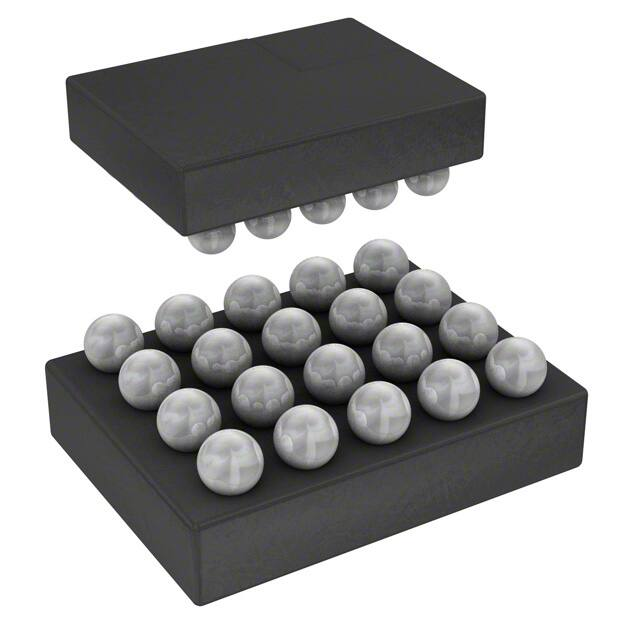
20-Bump WLCSP
Applications
Set-Top Box
Hard Disk Drive
Communications Cards
DSP Power
At moderate and light loads, pulse frequency modulation
(PFM) is used to operate the device in power-save mode
with a typical quiescent current of 50 µA. Even with such a
low quiescent current, the part exhibits excellent transient
response during large load swings. At higher loads, the
system automatically switches to fixed-frequency control,
operating at 2.4 MHz. In shutdown mode, the supply current
drops below 1 µA, reducing power consumption. PFM mode
can be disabled if constant frequency is desired. The
FAN53541 is available in a 20-bump 1.96 mm x 1.56 mm
Wafer-Level Chip-Scale Package (WLCSP).
PGOOD
VIN
CIN
10µF
L1
SW
CIN1
0.47H
10nF
FAN53541
GND
COUT
COUT
10µF
10µF
VOUT
EN
R1
FB
MODE
R2
Figure 1. Typical Application
Ordering Information
Part Number
Temperature Range
FAN53541UCX
-40 to 85°C
© 2013 Semiconductor Components Industries, LLC.
FAN53541 • Rev. 1.1
Package
20-Ball Wafer-Level, Chip-Scale Package (WLCSP),
4x5 Array, 0.4 mm Pitch, 250 µm Ball
Packing Method
Tape and Reel
www.fairchildsemi.com
www.onsemi.com
FAN53541 — 2.4MHz, 5A TinyBuck™ Synchronous Buck Regulator
May 2017
�Table 1. Recommended External Components for 5 A Maximum Load Current
Component
Description
Vendor
Parameter
Typical
Unit
L1
470 nH Nominal
See Table 2
L
0.47
H
COUT
10 F, 6.3V, X5R, 0805, 2 Pieces
C
20
F
CIN
10 F, 6.3 V, X5R, 0805
GRM21BR60J106M (Murata)
C2012X5R0J106M (TDK)
C
10
F
CIN1
10 nF, 25 V, X7R, 0402
Any
C
10
nF
Table 2. Recommended Inductors
Component Dimensions
DCR (mΩ) IMAXDC 1
( )
Manufacturer
Part#
L (nH)
Bourns
SRP5012-R47M
470
19
Bourns
SRP4012-R47M
470
20
L
W
H
6.0
5.1
4.5
1.2
5.5
4.6
4.0
1.2
Coilcraft
XPL4020-471ML
470
19
7.2
4.2
4.2
2.0
Inter-Technical(2)
SC2511-R47M
470
2.6
16.0
6.5
6.5
3.0
TDK
VLC5020T-R47M
470
15
5.4
5.0
5.0
2.0
Vishay
IHLP1616ABERR47M01
470
20
5.0
4.5
4.1
1.2
Notes:
1. IMAXDC is the lesser current to produce 40°C temperature rise or 30% inductance roll-off.
2. Inductor used for efficiency and temperature rise measurements.
© 2013 Semiconductor Components Industries, LLC.
FAN53541 • Rev. 1.1
2
www.fairchildsemi.com
www.onsemi.com
FAN53541 — 2.4 MHz, 5 A TinyBuck™ Synchronous Buck Regulator
Recommended External Components
�PGOOD
EN
FB
VOUT
A1
A2
A3
A4
A4
A3
A2
A1
MODE
GND
B1
B2
B3
B4
B4
B3
B2
B1
C1
C2
C3
C4
C4
C3
C2
C1
D1
D2
D3
D4
D4
D3
D2
D1
E1
E2
E3
E4
E4
E3
E2
E1
VIN
SW
Figure 2. Top View
Figure 3. Top View Bottom View
Pin Definitions
Bump #
Name
Description
A1
PGOOD
A2
EN
Enable. The device is in Shutdown Mode when this pin is LOW. Do not leave this pin floating.
A3
FB
FB. Connect to resistor divider. The IC regulates this pin to 0.8 V.
A4
VOUT
VOUT. Sense pin for VOUT. Connect directly to COUT.
B1
MODE
MODE / SYNC. A logic 0 allows the IC to automatically switch to PFM during light loads. When held
HIGH, the IC to stays in PWM Mode. The regulator also synchronizes its switching frequency to four
times (4X) the frequency provided on this pin (fMODE). Do not leave this pin floating.
B2, B3,
C1 – C4
GND
Ground. Low-side MOSFET is referenced to this pin. CIN and COUT should be returned with a minimal
path to these pins.
B4
AGND
D1, D2,
E1, E2
VIN
Power Input Voltage. Connect to input power source. Connect to CIN with minimal path.
D3, D4,
E3, E4
SW
Switching Node. Connect to inductor.
Power Good. This open-drain pin pulls LOW if the output falls out of regulation or is in soft-start.
Analog Ground. All signals are referenced to this pin. Avoid routing high dV/dt AC currents through
this pin.
© 2013 Semiconductor Components Industries, LLC.
FAN53541 • Rev. 1.1
3
www.fairchildsemi.com
www.onsemi.com
FAN53541 — 2.4 MHz, 5 A TinyBuck™ Synchronous Buck Regulator
Pin Configuration
�Stresses exceeding the absolute maximum ratings may damage the device. The device may not function or be operable above
the recommended operating conditions and stressing the parts to these levels is not recommended. In addition, extended
exposure to stresses above the recommended operating conditions may affect device reliability. The absolute maximum
ratings are stress ratings only.
Symbol
Parameter
SW, VIN Pins
VIN
Other Pins
Min.
Max.
-0.3
7.0(3)
Tied without Series Impedance
-0.3
4.5
Tied through Series Resistance ≥100
-0.3
VIN⁽4⁾
Human Body Model per JESD22-A114
2250
Charged Device Model per JESD22-C101
1500
Unit
V
ESD
Electrostatic Discharge
Protection Level
TJ
Junction Temperature
–40
+150
°C
TSTG
Storage Temperature
–65
+150
°C
+260
°C
TL
Lead Soldering Temperature, 10 Seconds
V
Note:
3. VIN slew rate is limited to 1 V/µs.
4. Lesser of 7 V or VIN+0.3 V.
Recommended Operating Conditions
The Recommended Operating Conditions table defines the conditions for actual device operation. Recommended operating
conditions are specified to ensure optimal performance to the datasheet specifications. ON Semiconductor does not
recommend exceeding them or designing to Absolute Maximum Ratings.
Symbol
Parameter
Min.
Typ.
Max.
Unit
VIN
Supply Voltage Range
2.7
5.5
V
VOUT
Output Voltage Range
0.8
90% Duty
Cycle
V
IOUT
Output Current
0
5
A
1.20
µH
L
CIN
COUT
Inductor
0.47
Input Capacitor
10
Output Capacitor
µF
20
µF
TA
Operating Ambient Temperature
-40
+85
°C
TJ
Operating Junction Temperature
-40
+125
°C
Typical
Unit
38(5)
°C/W
Thermal Properties
Symbol
JA
Parameter
Junction-to-Ambient Thermal Resistance
Note:
5. See Thermal Considerations in the Applications section.
© 2013 Semiconductor Components Industries, LLC.
FAN53541 • Rev. 1.1
4
www.fairchildsemi.com
www.onsemi.com
FAN53541 — 2.4 MHz, 5 A TinyBuck™ Synchronous Buck Regulator
Absolute Maximum Ratings
�Minimum and maximum values are at V IN=2.7 V to 5.5 V, and TA=-40°C to +85°C, unless otherwise noted. Typical values are
at TA=25°C, VIN=5 V, and VOUT=1.2 V.
Symbol
Parameter
Condition
Min.
Typ.
Max. Unit
ILOAD=0, MODE=0 (AUTO PFM/PWM)
15
50
200
µA
ILOAD=0, MODE=1 (Forced PWM)
8
30
100
mA
Power Supplies
IQ
Quiescent Current
I SD
Shutdown Supply Current
VUVLO
Under-Voltage Lockout Threshold
VUVHYST
Under-Voltage Lockout Hysteresis
EN=GND
0.1
10
µA
VIN Rising
2.67
2.80
V
VIN Falling
2.1
2.3
V
365
mV
Logic Pins
VIH
High-Level Input Voltage
VIL
Low-Level Input Voltage
VLHYST
IIN
1.05
V
0.4
Logic Input Hysteresis Voltage
140
Input Bias Current
Input Tied to GND or 1 kΩ Resistor to VIN
IOUTL
PGOOD Pull-Down Current
VPGOOD=0.4 V
IOUTH
PGOOD HIGH Leakage Current
VPGOOD=VIN
0.01
V
mV
1.00
1
µA
mA
0.01
1.00
µA
VOUT Regulation
VREF
Output Reference DC Accuracy,
Measured at FB Pin
TA=25°C, Forced PWM
0.792
0.800
0.808
V
TA=-40°C to 85°C, Forced PWM
0.787
0.800
0.813
V
AUTO PFM/PWM
0.784
0.800
0.824
V
VOUT
ILOAD
Load Regulation
MODE=VIN (Forced PWM)
–0.02
%/A
VOUT
VIN
Line Regulation
2.7 V ≤ VIN ≤ 5.5 V, IOUT(DC)=1.5 A
-0.16
%/V
FB Pin Leakage Current
FB=0.8 V
Transient Response
ILOAD Step 0.1 A to 1.5 A, tR=100 ns
IREF
1
nA
-30
mV
RDS(ON)P P-Channel MOSFET On Resistance
33
mΩ
RDS(ON)N N-Channel MOSFET On Resistance
28
mΩ
VOUT
Power Switch and Protection
ILIMPK
P-MOS Peak Current Limit
TLIMIT
Thermal Shutdown
THYST
Thermal Shutdown Hysteresis
VSDWN
Input OVP Shutdown
Open Loop
5.8
Closed Loop
8.8
A
8
A
155
°C
20
°C
6.1
V
5.5
5.8
V
2.1
2.4
3.0
MHz
525
600
700
kHz
Rising Threshold
Falling Threshold
7.5
Frequency Control
fSW
fMODE
Oscillator Frequency
MODE Pin Synchronization Range
External Square-Wave, 30% to 70% Duty
Cycle
Soft-Start and Output Discharge
tSS
RDIS
Regulator Enable to Regulated VOUT
(Rising PGOOD)
Output Discharge Resistance
© 2013 Semiconductor Components Industries, LLC.
FAN53541 • Rev. 1.1
EN=0 V
5
1.2
ms
175
Ω
www.fairchildsemi.com
www.onsemi.com
FAN53541 — 2.4 MHz, 5 A TinyBuck™ Synchronous Buck Regulator
Electrical Characteristics
�95%
95%
90%
90%
Efficiency
Efficiency
Unless otherwise specified; VIN=5 V, VOUT=1.2 V, VMODE=0 V, TA=25°C, circuit in Figure 1, and components per Table 1.
85%
80%
2.7 VIN
75%
85%
80%
-40C
75%
3.3 VIN
+25C
5.0 VIN
+85C
5.5 VIN
70%
70%
0
1000
2000
3000
4000
5000
0
1000
Load Current (mA)
3000
4000
Figure 5. Efficiency vs. ILOAD, 1.2 VOUT
95%
90%
90%
Efficiency
95%
85%
80%
2.7 VIN
75%
85%
80%
-40C
75%
3.3 VIN
+25C
5.0 VIN
+85C
5.5 VIN
70%
70%
0
1000
2000
3000
4000
5000
0
1000
Load Current (mA)
2000
3000
4000
5000
Load Current (mA)
Figure 6. Efficiency vs. ILOAD, 1.8 VOUT
Figure 7. Efficiency vs. ILOAD, 1.8 VOUT
100%
100%
95%
95%
Efficiency
Efficiency
5000
Load Current (mA)
Figure 4. Efficiency vs. ILOAD, 1.2 VOUT
Efficiency
2000
90%
85%
4.2 VIN
80%
90%
85%
-40C
80%
5.0 VIN
+25C
5.5 VIN
+85C
75%
75%
0
1000
2000
3000
4000
5000
0
Load Current (mA)
2000
3000
4000
5000
Load Current (mA)
Figure 8. Efficiency vs. ILOAD, 3.3 VOUT
© 2013 Semiconductor Components Industries, LLC.
FAN53541 • Rev. 1.1
1000
Figure 9. Efficiency vs. ILOAD, 3.3 VOUT
6
www.fairchildsemi.com
www.onsemi.com
FAN53541 — 2.4 MHz, 5 A TinyBuck™ Synchronous Buck Regulator
Typical Characteristics
�Unless otherwise specified; VIN=5 V, VOUT=1.2 V, VMODE=0 V, TA=25°C, circuit in Figure 1, and components per Table 1.
70
35
30
25
2.7 VIN
65
4.2 VIN
3.3 VIN
60
5.0 VIN
5.0 VIN
55
5.5 VIN
5.5 VIN
50
VOUT Shift (mV)
VOUT Shift (mV)
45
20
15
10
40
35
30
25
20
15
5
10
0
5
-5
-5
0
1000
2000
3000
4000
0
5000
1000
2000
3000
4000
Load Current (mA)
Load Current (mA)
Figure 10. Regulation, 1.2 VOUT
Figure 11. Regulation, 3.3 VOUT
1,400
1,400
1,200
1,200
1,000
1,000
Load Current (mA)
Load Current (mA)
0
800
600
400
PFM Exit
200
5000
800
600
400
PFM Exit
200
PFM Enter
PFM Enter
0
0
2.5
3.0
3.5
4.0
4.5
5.0
5.5
3.5
4.0
Input Voltage (V)
4.5
5.0
5.5
Input Voltage (V)
Figure 12. PFM / PWM Boundaries, 1.2 VOUT
Figure 13. PFM / PWM Boundaries, 3.3 VOUT
30
3,000
3.6VIN, Auto
3.6VIN, PWM
2,500
5.0VIN, Auto
Switching Frequency (KHz)
Output Ripple (mVpp)
25
5.0VIN, PWM
20
15
10
5
2,000
1,500
1,000
3.6VIN, Auto
5.0VIN, Auto
500
0
0
0
1000
2000
3000
4000
0
5000
Figure 14. Output Voltage Ripple
© 2013 Semiconductor Components Industries, LLC.
FAN53541 • Rev. 1.1
1000
2000
3000
4000
5000
Load Current (mA)
Load Current (mA)
Figure 15. Switching Frequency
7
www.fairchildsemi.com
www.onsemi.com
FAN53541 — 2.4 MHz, 5 A TinyBuck™ Synchronous Buck Regulator
Typical Characteristics
�60
50
50
40
Input Current (mA)
Input Current (A)
Unless otherwise specified; VIN=5 V, VOUT=1.2 V, VMODE=0 V, TA=25°C, circuit in Figure 1, and components per Table 1.
40
30
20
30
20
10
-40C
-40C
+25C
+25C
+85C
10
+85C
0
2.5
3.0
3.5
4.0
4.5
5.0
5.5
2.5
3.0
Input Voltage (V)
4.0
4.5
5.0
5.5
Input Voltage (V)
Figure 16. Quiescent Current, Auto Mode, EN=VIN
Figure 17. Quiescent Current, PMW Mode, EN=VIN
70
100%
1.2VOUT,
25mA Load
1.2VOUT,
1.0A Load
3.3VOUT,
1.0A Load
60
95%
50
90%
Efficiency
PSRR (dB)
3.5
40
30
85%
1.2 VOUT, L=SC2511
80%
1.2 VOUT, L=IHLP16
1.8 VOUT, L=SC2511
20
75%
10
70%
1.8 VOUT, L=IHLP16
3.3 VOUT, L=SC2511
10
100
1,000
10,000
100,000
3.3 VOUT, L=IHLP16
0
Frequency (Hz)
1000
2000
3000
4000
5000
Load Current (mA)
Figure 18. Power Supply Rejection (PSRR)
Figure 19. Inductor Efficiency Comparison, 5.0 VIN
Figure 20. Line Transient, 50 Load, tR=tF=10 s
Figure 21. Line Transient, ILOAD=1.0 A, tR=tF=10 s
© 2013 Semiconductor Components Industries, LLC.
FAN53541 • Rev. 1.1
8
www.fairchildsemi.com
www.onsemi.com
FAN53541 — 2.4 MHz, 5 A TinyBuck™ Synchronous Buck Regulator
Typical Characteristics
�Unless otherwise specified; VIN=5 V, VOUT=1.2 V, VMODE=0 V, TA=25°C, circuit in Figure 1, and components per Table 1.
Figure 22. Load Transient, 0.1-1.5 A Load,
tR=tF=100 ns
Figure 23. Load Transient, 0.1-3.0 A Load,
tR=tF=100 ns, COUT=2x22 F
Figure 24. Startup / Shutdown, No Load
Figure 25. Startup / Shutdown, 240 m Load,
COUT=2x22 F
Figure 26. Overload Protection and Recovery
Figure 27. Startup into Overload
© 2013 Semiconductor Components Industries, LLC.
FAN53541 • Rev. 1.1
9
www.fairchildsemi.com
www.onsemi.com
FAN53541 — 2.4 MHz, 5 A TinyBuck™ Synchronous Buck Regulator
Typical Characteristics
�The FAN53541 is a step-down switching voltage regulator
that delivers an adjustable output from an input voltage
supply of 2.7 V to 5.5 V. Using a proprietary architecture with
synchronous rectification, the FAN53541 is capable of
delivering up to 5 A at over 90% efficiency. The regulator
operates at a nominal frequency of 2.4 MHz at full load,
which reduces the value of the external components to
470 nH for the output inductor and 20 µF for the output
capacitor. High efficiency is maintained at light load with
single-pulse PFM Mode.
limits the COUT capacitance when a heavy load ( ILOAD(SS) ) is
applied during the startup.
The maximum COUT capacitance for successful starting with
a heavy constant-current load is approximately:
COUT
Under-Voltage Lockout (UVLO)
When EN is HIGH, the under-voltage lockout keeps the part
from operating until the input supply voltage rises high
enough to operate properly. This ensures no misbehavior of
the regulator during startup or shutdown.
Input Over-Voltage Protection (OVP)
For very light loads, the FAN53541 operates in
Discontinuous Current (DCM) single-pulse PFM Mode, which
produces low output ripple compared with other PFM
architectures. Transition between PWM and PFM is
seamless, with a glitch of less than 3% of VOUT during the
transition between DCM and CCM Modes.
When VIN exceeds VSDWN (about 6.1 V), the IC stops
switching to protect the circuitry from excessive internal
voltage spikes. An internal filter prevents the circuit from
shutting down due to VIN noise spikes.
Current Limiting
PFM Mode is disabled by holding the MODE pin HIGH. The
IC synchronizes to the MODE pin frequency. When
synchronizing to the MODE pin, PFM Mode is disabled.
A heavy load or short circuit on the output causes the current
in the inductor to increase until a maximum current threshold
is reached in the high-side switch. Upon reaching this point,
the high-side switch turns off, preventing high currents from
causing damage. 16 consecutive PWM cycles in current limit
cause the regulator to shut down and stay off for about
1.6 ms before attempting a restart.
Setting Output Voltage
The output voltage is set by the R1, R2, and VREF (0.8 V):
(1)
In the event of a short circuit, the soft-start circuit attempts to
restart and produces an over-current fault after 16
consecutive cycles in current limit, which results in a duty
cycle of less than 5%, providing current into a short circuit.
(2)
External Frequency Synchronization
R1 must be set at or below 100 KΩ; therefore:
R1 0.8
Logic 1 on the MODE pin forces the IC to stay in PWM
Mode. Logic 0 allows the IC to automatically switch to PFM
during light loads. If the MODE pin is toggled, the converter
synchronizes its switching frequency to four times the
frequency on the mode pin (fMODE).
For example, for VOUT=1.2 V, R1=100 kΩ, R2=200 kΩ.
Enable and Soft-Start
When the EN pin is LOW, the IC is shut down, all internal
circuits are off, and the part draws very little current. Raising
EN above its threshold voltage activates the part and starts
the soft-start cycle. During soft-start, the modulator’s internal
reference is ramped slowly to minimize surge currents on the
input and prevents overshoot of the output voltage.
The MODE pin is internally buffered with a Schmitt trigger,
which allows the MODE pin to be driven with slow rise and
fall times. An asymmetric duty cycle for frequency
synchronization is permitted, provided it is consistent with
parametric table limits.
If large values of output capacitance are used, the regulator
may fail to start. If VOUT fails to achieve regulation within
1.2 ms from the beginning of soft-start, the regulator shuts
down and waits 1.6 ms before attempting a restart. If the
regulator is in current limit for 16 consecutive PWM cycles,
the regulator shuts down before restarting 1.6 ms later. This
© 2013 Semiconductor Components Industries, LLC.
FAN53541 • Rev. 1.1
(3)
When EN is LOW, a 150 resistor discharges VOUT.
Regulator performance is independent of the output
capacitor ESR, allowing for the use of ceramic output
capacitors. Although this type of operation normally results in
a switching frequency that varies with input voltage and load
current, an internal frequency loop holds the switching
frequency constant over a large range of input voltages and
load currents.
VOUT 0.8
800
VOUT
Diode Emulation Mode is employed during soft-start,
allowing the IC to start into a pre-charged output. Diode
emulation prohibits reverse inductor current from flowing
through the synchronous rectifier.
The FAN53541 uses a proprietary non-linear, fixedfrequency PWM modulator to deliver very fast load transient
response, while maintaining a constant switching frequency
over a wide range of operating conditions.
R2
5.8 ILOAD
where COUTMAX is expressed in F and ILOAD is
the load current during soft-start, expressed in A.
Control Scheme
R1 VOUT VREF
R2
VREF
MAX
10
www.fairchildsemi.com
www.onsemi.com
FAN53541 — 2.4 MHz, 5 A TinyBuck™ Synchronous Buck Regulator
Operation Description
�Application Information
The PGOOD pin is an open-drain that indicates that the IC is
in regulation when its state is open. PGOOD pulls LOW
under the following conditions:
The IC has operated in cycle-by-cycle current limit for
eight consecutive PWM cycles;
The circuit is disabled, either after a fault occurs or when
EN is LOW; or
Selecting the Inductor
The output inductor must meet both the required inductance
and the energy handling capability of the application. The
inductor value affects the average current limit, output
voltage ripple, transient response, and efficiency.
The ripple current (∆I) of the regulator is:
The IC is performing a soft-start.
I
Thermal Shutdown
When the die temperature increases, due to a high load
condition and/or a high ambient temperature, the output
switching is disabled until the temperature on the die has
fallen sufficiently. The junction temperature at which the
thermal shutdown activates is nominally 155°C with a
20°C hysteresis.
IMAX (LOAD) ILIM(PK)
(5)
I
2
(6)
The FAN53541 is optimized for operation with L=470 nH, but
is stable with inductances up to 1.2 H (nominal). The
inductor should be rated to maintain at least 80% of its value
at ILIM(PK). Failure to do so lowers the amount of DC current
the IC can deliver.
tOFF(MIN) is 45 ns, which constrains the maximum VOUT/VIN
that the FAN53541 can provide, while still maintaining a fixed
switching frequency in PWM Mode. Regulation is maintained
even though the regulator is unable to provide sufficient
duty-cycle and operate at 2.4 MHz.
Efficiency is affected by the inductor DCR and inductance
value. Decreasing the inductor value for a given physical
size typically decreases the DCR; but since ∆I increases, the
RMS current increases, as do core and skin-effect losses.
Switching frequency is the lower of 2.4 MHz or:
The maximum average load current, I MAX(LOAD), is related to
the peak current limit, ILIM(PK), by the ripple current as:
Minimum Off-Time Effect on Switching
Frequency
VOUT IOUT ROFF
fSW (MHz) 22.2 1
V
IN IOUT (R OFF R ON )
VOUT VIN VOUT
VIN L fSW
IRMS
(4)
IOUT(DC ) 2
I2
12
(7)
The increased RMS current produces higher losses through
the RDS(ON) of the IC MOSFETs as well as the inductor ESR.
where:
Increasing the inductor value produces lower RMS currents,
but degrades transient response. For a given physical
inductor size, increased inductance usually results in an
inductor with lower saturation current.
IOUT = load current, in A;
RON = RDS(ON)_P + DCRL, in Ohms; and
ROFF = RDS(ON)_N + DCRL, in Ohms.
Table 3 shows the effects on regulator performance of higher
inductance than the recommended 470 nH.
A result of 0.4 mm wide trace is recommended. Avoid
routing this trace directly beneath SW unless separated by
an internal GND plane.
To minimize ESL, try to use capacitors with the lowest ratio
of length to width. 0805 s have lower ESL than 1206 s. If
very low output ripple is necessary, research vendors that
produce 0508 or 0612 capacitors with ultra-low ESL. Placing
additional small value capacitors near the load also reduces
the high-frequency ripple components.
If the MODE function is not required, extend the ground
plane through the MODE pin to reduce the loop inductance
for the VIN bypass.
Input Capacitor
The 10 F ceramic input capacitor should be placed as close
as possible between the VIN pin and PGND to minimize the
parasitic inductance. If a long wire is used to bring power to
the IC, additional “bulk” capacitance (electrolytic or tantalum)
should be placed between CIN and the power source lead to
reduce under-damped ringing that can occur between the
inductance of the power source leads and CIN.
Thermal Considerations
Heat is removed from the IC through the solder bumps to the
PCB copper. The junction-to-ambient thermal resistance
(JA) is largely a function of the PCB layout (size, copper
weight, and trace width) and the temperature rise from
junction to ambient (T).
The JA is 38°C/W when mounted on its four-layer evaluation
board in still air, with 2 oz. outer layer copper weight and
1 oz. inner layers. Halving the copper thickness results in an
increased JA of 48°C/W.
The effective CIN capacitance value decreases as VIN
increases due to DC bias effects. This has no significant
impact on regulator performance.
To reduce ringing and overshoot on VIN and SW, an
additional bypass capacitor CIN1 is recommended. Because
this lower value capacitor has a higher resonant frequency
than CIN; CIN1 should be placed closer to the VIN and GND
pins of the IC than CIN.
© 2013 Semiconductor Components Industries, LLC.
FAN53541 • Rev. 1.1
For long term reliable operation, the IC’s junction
temperature (TJ) should be maintained below 125°C.
Maximum IC power loss is 2.88 W. Figure 29 shows required
power dissipation and derating for a FAN53541 mounted on
the ON Semiconductor evaluation board in still air (38°C/W).
12
www.fairchildsemi.com
www.onsemi.com
FAN53541 — 2.4 MHz, 5 A TinyBuck™ Synchronous Buck Regulator
Output Capacitor and VOUT Ripple
�Maximum Power Dissipation (W)
3.0
2.88W, max.
2.5
2.0
1.5
1.0
0.5
E.
0
25
50
75
100
From Eq. (11), DCR


 工商网监
湘ICP备2023018690号
工商网监
湘ICP备2023018690号
