Is Now Part of
To learn more about ON Semiconductor, please visit our website at
www.onsemi.com
Please note: As part of the Fairchild Semiconductor integration, some of the Fairchild orderable part numbers
will need to change in order to meet ON Semiconductor’s system requirements. Since the ON Semiconductor
product management systems do not have the ability to manage part nomenclature that utilizes an underscore
(_), the underscore (_) in the Fairchild part numbers will be changed to a dash (-). This document may contain
device numbers with an underscore (_). Please check the ON Semiconductor website to verify the updated
device numbers. The most current and up-to-date ordering information can be found at www.onsemi.com. Please
email any questions regarding the system integration to Fairchild_questions@onsemi.com.
ON Semiconductor and the ON Semiconductor logo are trademarks of Semiconductor Components Industries, LLC dba ON Semiconductor or its subsidiaries in the United States and/or other countries. ON Semiconductor owns the rights to a number
of patents, trademarks, copyrights, trade secrets, and other intellectual property. A listing of ON Semiconductor’s product/patent coverage may be accessed at www.onsemi.com/site/pdf/Patent-Marking.pdf. ON Semiconductor reserves the right
to make changes without further notice to any products herein. ON Semiconductor makes no warranty, representation or guarantee regarding the suitability of its products for any particular purpose, nor does ON Semiconductor assume any liability
arising out of the application or use of any product or circuit, and specifically disclaims any and all liability, including without limitation special, consequential or incidental damages. Buyer is responsible for its products and applications using ON
Semiconductor products, including compliance with all laws, regulations and safety requirements or standards, regardless of any support or applications information provided by ON Semiconductor. “Typical” parameters which may be provided in ON
Semiconductor data sheets and/or specifications can and do vary in different applications and actual performance may vary over time. All operating parameters, including “Typicals” must be validated for each customer application by customer’s
technical experts. ON Semiconductor does not convey any license under its patent rights nor the rights of others. ON Semiconductor products are not designed, intended, or authorized for use as a critical component in life support systems or any FDA
Class 3 medical devices or medical devices with a same or similar classification in a foreign jurisdiction or any devices intended for implantation in the human body. Should Buyer purchase or use ON Semiconductor products for any such unintended
or unauthorized application, Buyer shall indemnify and hold ON Semiconductor and its officers, employees, subsidiaries, affiliates, and distributors harmless against all claims, costs, damages, and expenses, and reasonable attorney fees arising out
of, directly or indirectly, any claim of personal injury or death associated with such unintended or unauthorized use, even if such claim alleges that ON Semiconductor was negligent regarding the design or manufacture of the part. ON Semiconductor
is an Equal Opportunity/Affirmative Action Employer. This literature is subject to all applicable copyright laws and is not for resale in any manner.
�FAN5646
Programmable Indicator ―Soft‖ LED Blinker with TinyWire™
Single-Wire Interface
Features
Description
LED “Soft” Blink: with Logarithmic Fade Up and Fade
Down for Power Savings
Follow or Repeat Pattern Mode for Blinking when
Applications Processor is Powered Down
Default Pattern Optionally Modified using TinyWire™
Single-Wire Digital Control for:
– LED Current Rise / Fall Time
– tON and tOFF for Up to Two Pulses
The FAN5646 is a flexible and compact solution for a blinking
or “breathing” LED indicator. The internal programmable blink
algorithm eliminates any need for continual system processor
control. This means longer battery life for a hand-held system
because the system processor is not awakened from sleep
mode to blink an LED.
High-Side Constant Current LED Driver:
– 20 mA Maximum Output Current
– 80 mV Drop-out at 20 mA IOUT
– External RSET (SC70 only) or Internal Current
Programming
35 A Operating Quiescent Current
Short-Circuit, Under-Voltage, and Thermal Protections
Very low dropout of 80 mV allows driving an LED without any
inductors or switch capacitors. LED blink rate, rise and fall
time, and CTRL line behavior can be programmed by a
TinyWire™ single-wire digital interface. The on-time and time
between pulses can be set for up to two different pulse widths.
The default for FAN5646 option 01 is “follow” mode, where the
LED turns on with the programmed rise time, then stays on as
long as CTRL remains HIGH. When CTRL falls, the LED turns
off at the programmed fall time. For option 00; when CTRL is
HIGH continuously, the LED repeats the programmed pattern.
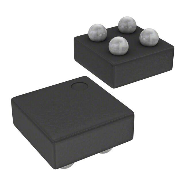
The FAN5646 is available in a four-pin wafer-level chip-scale
package with 0.4 mm pitch or a five-lead SC70 package.
Wide Input Range: 2.7 to 5.5 V
4-Bump WLCSP, 0.4 mm pitch or
5-Lead SC70 (EIAJ SC88)
VIN
2.7 to 5.5V
0.1
GND
Applications
1
5
2
ISET
3
Cell Phone
Pocket PCs and Digital Cameras
LED+
4
CTRL
R=24.3kW
Bluetooth® Headsets PMP and MP3 players
Figure 1. Typical Application
Ordering Information
Part Number
Option Follow Bit Default Temperature Range
Package
Packing
FAN5646UC00X
00
0
-40 to 85°C
WLCSP-4, 0.4mm Pitch
Tape and Reel
FAN5646S700X
00
0
-40 to 85°C
5-Lead SC70, EIAJ SC88 Tape and Reel
FAN5646UC01X
01
1
-40 to 85°C
WLCSP-4, 0.4mm Pitch
FAN5646S701X
01
1
-40 to 85°C
5-Lead SC70, EIAJ SC88 Tape and Reel
Tape and Reel
Bluetooth® is a registered trademark of Bluetooth SIG, Inc.
Important: Contact a Fairchild Semiconductor sales representative for additional performance information and specifications.
© 2009 Fairchild Semiconductor Corporation
FAN5646 • Rev. 1.0.3
www.fairchildsemi.com
FAN5646 — Programmable Indicator ―Soft‖ LED Blinker with TinyWire™ Interface
May 2013
�VIN
A1
A2
LED+
LED+
A2
A1
VIN
GND
B1
B2
CTRL
CTRL
B2
B1
GND
Figure 2. WLCSP – Top View: Bumps Facing Down
Figure 3. WLCSP – Bottom View: Bumps Facing Up
VIN 1
5 LED+
GND 2
ISET 3
4 CTRL
Figure 4. SC70-5 Top View
Pin Definitions
Pin #
Name
Description
WLCSP
SC70-5
A1
1
VIN
A2
5
LED+
LED Anode. LED current source output.
B1
2
GND
Ground.
B2
4
CTRL
Control pin. Logic input that controls programming and starts IC playback.
3
ISET
LED Current Setting. Full-scale LED current is set by tying this pin through a
resistor (RSET) to GND. If this pin is left open, an internal current reference is used.
© 2009 Fairchild Semiconductor Corporation
FAN5646 • Rev. 1.0.3
Input Voltage. Connect to 2.7-5.5 VDC input power source.
www.fairchildsemi.com
2
FAN5646 — Programmable Indicator ―Soft‖ LED Blinker with TinyWire™ Interface
Pin Configuration
�Stresses exceeding the absolute maximum ratings may damage the device. The device may not function or be operable above
the recommended operating conditions and stressing the parts to these levels is not recommended. In addition, extended
exposure to stresses above the recommended operating conditions may affect device reliability. The absolute maximum ratings
are stress ratings only.
Symbol
VCC
ESD
Parameter
Min.
Max.
Units
VIN, LED+, CTRL Voltage
-0.3
6.0
V
ISET Voltage
-0.3
VIN +
0.3
V
Electrostatic Discharge Protection Level
Human Body Model per JESD22-A114
8.0
Charged Device Model per JESD22-C101
2.0
kV
TJ
Junction Temperature
–40
+150
°C
TSTG
Storage Temperature
–65
+150
°C
+260
°C
TL
Lead Soldering Temperature, 10 Seconds
Recommended Operating Conditions
The Recommended Operating Conditions table defines the conditions for actual device operation. Recommended operating
conditions are specified to ensure optimal performance to the datasheet specifications. Fairchild does not recommend exceeding
them or designing to absolute maximum ratings.
Symbol
Parameter
Min.
Max.
Units
VIN
Power Supply Voltage Range
2.7
5.5
V
TA
Operating Ambient Temperature Range
-40
+85
°C
TJ
Operating Junction Temperature Range
-40
+125
°C
mA
ILED(FS)
RSET
Full-Scale LED Current
If ISET is OPEN
(1)
RSET Values for +10% ISET Accuracy
5
20
CONTROL[7:6] = 00
ILED = 7.2 mA to 2.5 mA
17.4
48.7
CONTROL[7:6] = 01
ILED = 12.1 mA to 7.1 mA
20.5
34.8
CONTROL[7:6] = 10
ILED = 17.3 mA to 12.3 mA
21.5
30.1
CONTROL[7:6] = 11
ILED = 20.4 mA to 17.3 mA
24.3
28.7
kΩ
Note:
1. Applicable for SC70 version only.
© 2009 Fairchild Semiconductor Corporation
FAN5646 • Rev. 1.0.3
www.fairchildsemi.com
3
FAN5646 — Programmable Indicator ―Soft‖ LED Blinker with TinyWire™ Interface
Absolute Maximum Ratings
�VIN = 2.7 V to 5.5 V, TA = -40°C to +85°C, Vf = 1.8 V to [ 3.5 V or VIN – 0.1 V ], whichever is smaller. Typical values are at
TA = 25°C, VIN = 3.6 V, and Vf = 2.5 V.
Symbol
Parameter
Conditions
Min.
Typ.
Max.
Units
VIN = 3.6 V, CTRL = 0 V
0.30
0.75
µA
VIN = 3.6 V, ILED = 0 mA
35
80
µA
VIN = 3.6 V, LED+ = ON
220
Power Supplies
ISD
IDLE Mode Supply Current
IIN
Quiescent Current
IACTIVE
Active Mode Supply Current
(2)
µA
VIH
Logic Input Voltage HIGH
VIL
Logic Input Voltage LOW
IIH
Control Pin Input Current
CTRL = 1.8 V
Under-Voltage Lockout
Threshold
VIN Rising
2.5
V
VIN Falling
2.2
V
VUVLO
1.1
V
1
0.4
V
250
nA
Regulation
ISET OPEN
ILED
LED Output
Current
4.25
5.00
5.75
CONTROL[7:6] = 01
8.70
10.00
11.30
CONTROL[7:6] = 10
13.20
15.00
16.80
CONTROL[7:6] = 11
18.00
20.00
22.00
CONTROL[7:6] = 00
4.70
5.00
5.30
CONTROL[7:6] = 01
9.40
10.00
10.60
CONTROL[7:6] = 10
14.10
15.00
15.90
CONTROL[7:6] = 11
18.80
20.00
21.20
mA
RSET = 24.3kW
VISET
CONTROL[7:6] = 00
ISET Drive Voltage
12.1 kΩ ≤ RSET ≤ 100 kΩ
1.23
V
0.5
% p-p
IOUT_RIPPLE
VIN = 3.6 V, ΔVIN = 700 mV,
Maximum LED Ripple Current(2) ILED = 20 mA, trise = tfall = 10 µs,
tLOW = 280 µs
∆IOUT_LOAD
IOUT Load Regulation
LED Vf = 1.8 to 3.45 V, VIN = 3.6 V
-3
+3
%
∆IOUT_LINE
IOUT Line Regulation
VIN = 2.7 to 4.8 V, Vf = 2.5 V
-3
+3
%
VDROPOUT
Dropout Voltage
ILED = 20 mA, -10% ILED Drop
80
Rising Temperature at Junction
150
Hysteresis
20
TSD
mV
Thermal Shutdown
°C
Timing
fOSC
Internal Oscillator Frequency
TOSC
Oscillator Stability Over
Temperature(2)
VIN = 3.6 V
61
77
3
93
kHz
%
Note:
2. These parameters are guaranteed by design and characterization.
© 2009 Fairchild Semiconductor Corporation
FAN5646 • Rev. 1.0.3
www.fairchildsemi.com
4
FAN5646 — Programmable Indicator ―Soft‖ LED Blinker with TinyWire™ Interface
Electrical Specifications
�300
90
280
80
260
70
240
IIN [µA]
Efficiency [%]
100
60
50
40
VF = 3.3V
IOUT = 15mA
30
20
25°C
85°C
220
200
-40°C
180
160
140
120
10
100
2.50
0
3.00
3.50
4.00
4.50
5.00
5.50
3.00
VIN [V]
4.50
5.00
5.50
Figure 6. Active Mode Supply Current (LED+ = ON)
60
25
50
20
ILED [mA]
85°C
25°C
40
IIN [µA]
4.00
VIN [V]
Figure 5. Efficiency at 25C
30
-40°C
20
25°C
15
10
5
10
-40°C
85°C
0
0
2.50
3.00
3.50
4.00
4.50
5.00
5.50
Figure 7. Quiescent Current (ILED = 0 mA)
22
20
18
16
14
12
10
8
6
4
2
0
0
100
200
300
0.00 0.01 0.02 0.03 0.04 0.05 0.06 0.07 0.08 0.09 0.10
VIN - VOUT [V]
VIN [V]
ILED [mA]
3.50
400
Figure 8. Output Current vs. Headroom Voltage
500
RSET [kW]
Figure 9. Output Current vs. RSET at 25C
© 2009 Fairchild Semiconductor Corporation
FAN5646 • Rev. 1.0.3
www.fairchildsemi.com
5
FAN5646 — Programmable Indicator ―Soft‖ LED Blinker with TinyWire™ Interface
Typical Characteristics
�Operating Modes
Play and Follow Bits
Table 3. PLAY and FOLLOW Bit Definition
PLAY
FOLLOW
Behavior
0
0
Default Behavior per Table 1*
0
1
LED Follows CTRL**
1
0
LED Enters PLAY Mode
1
1
LED Enters One-Shot Mode
TOFF2
TON2
TOFF1
TON1
TOFF2
TON2
INITIAL 1.7s
TOFF1
At power up, the device is in IDLE (“sleep”) Mode until a rising
edge of a CTRL signal is detected. When both the PLAY and
FOLLOW bits are 0, the FAN5646 executes the LED pattern
shown in Figure 10. If the length of the CTRL pulse is less
than 1.7 s, only the initial pulse is seen. A CTRL pulse that is
kept HIGH after the initial 1.7 s pulse causes the FAN5646 to
go into PLAY mode where PULSE1 and PULSE2 are played
as programmed in the registers (see Table 9).
LED
One-Shot Mode
This mode is enabled when the PLAY and FOLLOW bits are
both 1. One-Shot Mode is similar to PLAY mode except that
PULSE1 is enabled while PULSE2 is always ignored. In OneShot Mode, PULSE1 is played after CTRL is held HIGH for at
least 200 s. Once PULSE1 is initiated, CTRL is ignored until
PULSE1 is completed. If CTRL remains HIGH through the tOFF
time of PULSE1, PULSE1 continues to replay until CTRL is
lowered. Therefore, One-Shot Mode enables the LED to blink
in the programmed pattern as long as CTRL is HIGH.
CTRL
Figure 10. Initial Pulse Mode Timing
Table 1. CTRL Pin Operation, CONTROL[1:0] = 00
Mode
LED
Entry
IDLE
OFF
CTRL LOW for > 200 s
PLAY
Play Pattern
CTRL HIGH > 2 s
FOLLOW
Follows CTRL
CTRL HIGH < 2 s
Program
OFF
CTRL HIGH < 50 s
t RISE
t ON
t FALL
t OFF
The behavior described in Table 1 can be changed using the
PLAY and FOLLOW bits (see Table 3).
Figure 11. LED Average Current Profile
In PLAY Mode, the default pattern of PULSE1 repeats when
CTRL is held HIGH while PULSE2 is always ignored (see
Table 2). The FAN5646 plays the programmed sequence for
blinking the LED until CTRL is set LOW. The programmed
LED pattern always starts with PULSE1 and it can have tON
and tOFF times that are multiples of 106ms (see Equation (4))
while PULSE2 is disabled when its respective tON and tOFF
times are set to zero.
Table 4. Brightness Steps during Fade Up/Down (12.5%)
IOUT(DC) = 12.5% of Full Scale
Table 2. PULSE1 Default Pattern – PLAY Mode
tRISE
tFALL
tON
tOFF
516ms
516ms
533ms
1600ms
The IC creates the rise and fall profiles in Figure 11 by
stepping through PWM dimming values given in Table 4 and
Table 5. The SLEW1 and SLEW2 registers control the
brightness of the LED for PULSE1 and PULSE2, respectively.
In the example in Table 2, only the SLEW1 register is
programmed with the brightness level for the LED.
Step #
tON (s)
tOFF (s)
% of Full Power
0
1
2
3
4
5
6
7
0
13
65
156
299
482
716
1,016
3,333
3,320
3,268
3,177
3,034
2,852
2,617
2,318
0.00%
0.05%
0.24%
0.60%
1.10%
1.80%
2.70%
3.80%
In FOLLOW Mode, the LED+ pin is ON when CTRL is HIGH
and, as such, follows the CTRL signal applied to FAN5646.
*
**
© 2009 Fairchild Semiconductor Corporation
FAN5646 • Rev. 1.0.3
Default setting for FAN5646_00
Default setting for FAN5646_01
www.fairchildsemi.com
6
FAN5646 — Programmable Indicator ―Soft‖ LED Blinker with TinyWire™ Interface
Circuit Description
�Table 6. LED Maximum Current, WLCSP or ISET Open
ISET Bits
IOUT(DC) = 100% of Full Scale
ILED(MAX) (mA)
***
Step #
tON (s)
tOFF (s)
00
% of Full
Power
5
01
10
10
15
11
20
8
169
3,164
5.1%
9
221
3,112
6.6%
10
273
3,060
8.2%
11
339
2,995
10.2%
12
417
2,917
12.5%
13
495
2,839
14.8%
14
586
2,747
17.6%
15
677
2,656
20.3%
16
781
2,552
23.4%
ISET Bits
K
17
885
2,448
26.6%
00***
123
18
1,003
2,331
30.1%
01
246
19
1,133
2,201
34.0%
10
369
20
1,276
2,057
38.3%
11
492
21
1,419
1,914
42.6%
22
1,563
1,771
46.9%
23
1,732
1,602
52.0%
24
1,901
1,432
57.0%
25
2,070
1,263
62.1%
26
2,266
1,068
68.0%
27
2,461
872
73.8%
28
2,669
664
80.1%
29
2,878
456
86.3%
30
3,099
234
93.0%
31
3,333
0
100.0%
ILED can be programmed with an external RSET resistor to GND
in conjunction with the ISET bits:
I LED
K
RSET 200
RSET
K
I LED
or
(1)
200
Table 7. LED Programming RSET
RSET should be between 12.1 kW and 100 kW, which
corresponds to a range of 20 mA and 2.5 mA respectively
when the ISET bits are 01 and ILED(max) = 10 mA. To achieve
the highest accuracy using an external RSET, program the
ISET bits for the ILED closest to the desired ILED based on the
ISET values in Table 6. Then calculate the appropriate RSET
for the desired ISET using Equation (1) with the K value for
the chosen ISET bit value from Table 7.
RISE and FALL
The IC creates the rise and fall profiles in Figure 11 by
incrementing or decrementing the PWM dimming value at a
rate determined by the SLEW1 and SLEW2 registers. tRISE or
tFALL are determined by the following equation:
Changing the Default Values
tRISE 31 NRISE 3.33ms
(2)
tFALL 31 NFALL 3.33ms
(3)
where NRISE and NFALL are decimal values in the SLEW
registers (Table 9). Therefore, the maximum time for rise or
fall time to or from full current is:
The default values for the customer-accessible registers
produce the fixed tON, tOFF, tRISE, and tFALL illustrated in Table 2.
These values can be changed using registers (see Table 9)
accessible through the TinyWire™ single-wire interface.
tRISE/FALL (max) = 1550ms
The PLAY and FOLLOW control bits define the FAN5646 IC
behavior (Table 1) of the CTRL line. In addition, the full-scale
LED current can be changed (Table 6).
If the value of NRISE or NFALL is 0, the LED goes to (or from) off
to full brightness with no brightness ramp. Therefore, the
minimum time for controlled brightness stepping to full current
(NRISE = 1) is:
LED Full-Scale Current
The full-scale LED current can be set using the ISET bits
(CONTROL[7:6]) to accommodate a wide variety of LEDs.
tRISE/FALL (min) = 103 ms
PULSE1 and PULSE2 have independently programmable
tRISE and tFALL.
When CTRL first goes HIGH, the IC determines if an RSET is
connected. If the ISET is open or shorted to ground, ILED is set
by an internal reference according to Table 6:
© 2009 Fairchild Semiconductor Corporation
FAN5646 • Rev. 1.0.3
***
Default setting for the ISET bits.
www.fairchildsemi.com
7
FAN5646 — Programmable Indicator ―Soft‖ LED Blinker with TinyWire™ Interface
Table 5. Brightness Steps During Fade Up/Down (100%)
�The FAN5646 is capable of two pulses of different lengths with
independently programmable tON, tRISE, and tFALL. The time
between each of these pulses is established by tOFF.
t ON (SLOW 1) N _ ON 106.6ms
(4)
t OFF (SLOW 1) N _ OFF 320ms
(5)
where SLOW is the value of the SLOW bit (CONTROL[2] –
register), which is 1 or 0. N_ON and N_OFF values are
PULSE1 and PULSE2 register values (Table 9).
SLOW Bit
Maximum
Units
tON
0
1600
ms
tOFF
0
4800
ms
tON
1
3200
ms
tOFF
1
9600
ms
If tON is 0, the LED current ramps down immediately after
attaining its FINAL value. The minimum tON and tOFF for
PULSE1 is 6.7 ms, while PULSE2 is disabled when either tON
or tOFF is 0.
If N_ONPULSE2 and N_OFFPULSE2 are both 0, only the tON_PULSE1
and tOFF_PULSE1 are considered.
Table 9. Register Definition
Register
Address
(Hex)
Default
(Hex)
SLEW1
0
55
NRISE1: Duration of each brightness
level during LED turn-on
NFALL1: Duration of each brightness level
during LED turn-off
PULSE1
1
55
N_ON1: Duration the LED stays on at
100% brightness
N_OFF1: Duration the LED stays off after
ramping down
SLEW2
2
55
NRISE2: Duration of each brightness
level during LED turn-on
NFALL2: Duration of each brightness level
during LED turn-off
PULSE2
3
00
N_ON2: Duration the LED stays on at
100% brightness
N_OFF2: Duration the LED stays off after
ramping down
CONTROL
4
00(3)
01(4)
7
6
5
ISET
4
3
RESERVED
2
SLOW
1
PLAY
0
FOLLOW
Notes:
3. Default value for FAN5646_00.
4. Default value for FAN5646_01.
© 2009 Fairchild Semiconductor Corporation
FAN5646 • Rev. 1.0.3
www.fairchildsemi.com
8
FAN5646 — Programmable Indicator ―Soft‖ LED Blinker with TinyWire™ Interface
Table 8. tON and tOFF Maximum Values
tON and tOFF
�The example in Table 10 and Figure 12 illustrates the
relationship between the default register contents and the
pattern of the IC in PLAY mode. BOLD signifies the decimal
values of the controlling registers.
The example in Table 11 and Figure 13 illustrates a longduration pulse followed by a short-duration pulse with two
seconds between each pulse; with rise and fall times of each
using default values.
Table 10. PULSE1 Default Example (see Table 2 and
Table 9)
Table 11. Long-Short Pattern Example (see Figure 13)
tFALL1 = tRISE1 = 31 5 3.33 ms = 516 ms
tFALL1 = tRISE1 = 31 5 3.33 ms = 516 ms
tON1 = 10 106.6 ms =1066 ms
tON1 = 5 106.6 ms =533 ms
tOFF1 = 9 320 ms =2880 ms
tOFF1 = 5 320 ms =1600 ms
Register
SLEW1 PULSE1
Value
(HEX)
55
tFALL2 = tRISE2 = 31 1 3.33 ms = 103 ms
SLEW2
PULSE2
CONTROL
00
00
02
55
tON2 = 2 106.6 ms =213 ms
tOFF2= 5 320 ms =1600 ms
Register
516ms
533ms
516ms
1600ms
SLEW1 PULSE1 SLEW2
Value
(HEX)
55
103ms
213ms
A9
PULSE2
CONTROL
25
02
11
PULSE1
Figure 12. PULSE1 Default LED Current Pattern for
Register in Table 10
516ms
1066ms
516ms
2880ms
PULSE1
103ms
PULSE2
1600ms
PULSE1
Figure 13. LED Current Waveform for Register Settings in Table 11
© 2009 Fairchild Semiconductor Corporation
FAN5646 • Rev. 1.0.3
www.fairchildsemi.com
9
FAN5646 — Programmable Indicator ―Soft‖ LED Blinker with TinyWire™ Interface
Programming Examples
�TinyWire is a flexible, general-purpose, binary protocol
designed to minimize the number of pins on the IC while
providing a complete digital interface that can be driven from
any microcontroller or applications processor using “bit
banging” on a general-purpose I/O pin. The interface’s speed
and flexibility accommodate a wide range of processor clock
capabilities. The fully static nature of the interface requires that
the applications processor dedicate only sufficient
uninterrupted attention to bit banging to complete a single
packet. Interrupted packets are ignored and may be
subsequently retransmitted.
Data is written to the selected register at the rising edge of the
STOP bit. A new CONTROL word may start within 4 s of the
falling edge of the STOP bit.
As indicated in Table 1, if CTRL remains LOW for at least
tRESET after the falling edge of the STOP bit, the IC reverts to
its IDLE state.
If CTRL remains HIGH for at least tRESET, the IC executes its
programmed commands.
CONTROL Word
The CONTROL word contains the address of the register that
receives the data, followed by the data to be written. The
CONTROL word is shifted LSB first on the CTRL line, as
shown in Figure 14. The TinyWire protocol operates over a
wide range of tBIT times (see Table 13), allowing encoding of
the brightness control bit-stream using a microcontroller
software “bit-bang” loop.
The CONTROL word contains the address of the register to
receive the data followed by the data to be written. The
FAN5646 data transfer is an 11-bit word, with the first three
bits (0 through 2) being the register address, LSB first. The
next eight bits (3 through 10) are the data to be written to the
selected register, LSB first. Data is latched into the selected
register at the rising edge of the STOP bit. A new word may
be transferred to the IC as little as 4s after the falling edge of
the STOP bit.
The CONTROL word begins with the rising edge of CTRL. If
CTRL is HIGH for a greater percentage of the time than it is
LOW between rising edges, the bit is a 1. Conversely, if CTRL
is LOW longer than it is HIGH, the bit is a 0. Observe the
following timing rules to ensure proper data transmission:
Table 14 shows the CONTROL word structure as well as an
example of writing 23H into register 2 (A[2:0] = 010).
Table 14. Address and Data Word
Table 12. Data Bit Definition
BIT =
tLOW
tHIGH
BIT
0
> 75% tBIT
< 25% tBIT
Value
1
< 25% tBIT
> 75% tBIT
Example
0
1
2
3
4
5
6
7
8
9 10
A0 A1 A2 D0 D1 D2 D3 D4 D5 D6 D7
0
1
0
1
1
0
0
0
1
0
0
Table 13. Timing Requirements
Minimum
Maximum
tLOW
500 ns
40 s
tHIGH
500 ns
40 s
tRESET
200 s
DATA
LATCHED
t HIGH
LOGIC 0
LOGIC 1
t LOW
IDLE
t BIT
t BIT
t RESE T
BIT 0
BIT 1
BIT N
STOP BIT
Figure 14. TinyWire™ Protocol
© 2009 Fairchild Semiconductor Corporation
FAN5646 • Rev. 1.0.3
www.fairchildsemi.com
10
FAN5646 — Programmable Indicator ―Soft‖ LED Blinker with TinyWire™ Interface
TinyWire™ Digital Interface
�F
0.03 C
A
E
2X
0.40
B
Ø0.20
Cu Pad
A1
0.40
D
BALL A1
INDEX AREA
Ø0.30
Solder Mask
0.03 C
2X
TOP VIEW
RECOMMENDED LAND PATTERN
(NSMD PAD TYPE)
0.06 C
0.625
0.547
0.05 C
C
0.378±0.018
0.208±0.021
E
SEATING PLANE
SIDE VIEWS
D
NOTES:
A. NO JEDEC REGISTRATION APPLIES.
0.005
Ø0.260±0.020
4X
0.40
B
A
0.40
(Y)±0.018
1 2
B. DIMENSIONS ARE IN MILLIMETERS.
C. DIMENSIONS AND TOLERANCE
PER ASME Y14.5M, 1994.
D. DATUM C IS DEFINED BY THE SPHERICAL
CROWNS OF THE BALLS.
E. PACKAGE NOMINAL HEIGHT IS 586 MICRONS
±39 MICRONS (547-625 MICRONS).
(X)±0.018
F
BOTTOM VIEW
C A B
F. FOR DIMENSIONS D, E, X, AND Y SEE
PRODUCT DATASHEET.
G. DRAWING FILNAME: MKT-UC004ACrev2.
Figure 15. 4-Bump WLCSP, 0.4 mm Pitch
Product-Specific Dimensions
Product
D
E
X
Y
FAN5646UC
0.820 mm
0.820 mm
0.210 mm
0.210 mm
Package drawings are provided as a service to customers considering Fairchild components. Drawings may change in any manner without
notice. Please note the revision and/or date on the drawing and contact a Fairchild Semiconductor representative to verify or obtain the most
recent revision. Package specifications do not expand the terms of Fairchild’s worldwide terms and conditions, specifically the warranty therein, which
covers Fairchild products.
Always visit Fairchild Semiconductor’s online packaging area for the most recent package drawings:
http://www.fairchildsemi.com/packaging/.
© 2009 Fairchild Semiconductor Corporation
FAN5646 • Rev. 1.0.3
www.fairchildsemi.com
11
FAN5646 — Programmable Indicator ―Soft‖ LED Blinker with TinyWire™ Interface
Physical Dimensions
�FAN5646 — Programmable Indicator ―Soft‖ LED Blinker with TinyWire™ Interface
Physical Dimensions (Continued)
Figure 16. 5-Lead SC70 (EIAJ SC88)
Package drawings are provided as a service to customers considering Fairchild components. Drawings may change in any manner without
notice. Please note the revision and/or date on the drawing and contact a Fairchild Semiconductor representative to verify or obtain the most
recent revision. Package specifications do not expand the terms of Fairchild’s worldwide terms and conditions, specifically the warranty therein, which
covers Fairchild products.
Always visit Fairchild Semiconductor’s online packaging area for the most recent package drawings:
http://www.fairchildsemi.com/packaging/.
© 2009 Fairchild Semiconductor Corporation
FAN5646 • Rev. 1.0.3
www.fairchildsemi.com
12
�FAN5646 — Programmable Indicator ―Soft‖ LED Blinker with TinyWire™ Interface
© 2009 Fairchild Semiconductor Corporation
FAN5646 • Rev. 1.0.3
www.fairchildsemi.com
13
�ON Semiconductor and
are trademarks of Semiconductor Components Industries, LLC dba ON Semiconductor or its subsidiaries in the United States and/or other countries.
ON Semiconductor owns the rights to a number of patents, trademarks, copyrights, trade secrets, and other intellectual property. A listing of ON Semiconductor’s product/patent
coverage may be accessed at www.onsemi.com/site/pdf/Patent−Marking.pdf. ON Semiconductor reserves the right to make changes without further notice to any products herein.
ON Semiconductor makes no warranty, representation or guarantee regarding the suitability of its products for any particular purpose, nor does ON Semiconductor assume any liability
arising out of the application or use of any product or circuit, and specifically disclaims any and all liability, including without limitation special, consequential or incidental damages.
Buyer is responsible for its products and applications using ON Semiconductor products, including compliance with all laws, regulations and safety requirements or standards,
regardless of any support or applications information provided by ON Semiconductor. “Typical” parameters which may be provided in ON Semiconductor data sheets and/or
specifications can and do vary in different applications and actual performance may vary over time. All operating parameters, including “Typicals” must be validated for each customer
application by customer’s technical experts. ON Semiconductor does not convey any license under its patent rights nor the rights of others. ON Semiconductor products are not
designed, intended, or authorized for use as a critical component in life support systems or any FDA Class 3 medical devices or medical devices with a same or similar classification
in a foreign jurisdiction or any devices intended for implantation in the human body. Should Buyer purchase or use ON Semiconductor products for any such unintended or unauthorized
application, Buyer shall indemnify and hold ON Semiconductor and its officers, employees, subsidiaries, affiliates, and distributors harmless against all claims, costs, damages, and
expenses, and reasonable attorney fees arising out of, directly or indirectly, any claim of personal injury or death associated with such unintended or unauthorized use, even if such
claim alleges that ON Semiconductor was negligent regarding the design or manufacture of the part. ON Semiconductor is an Equal Opportunity/Affirmative Action Employer. This
literature is subject to all applicable copyright laws and is not for resale in any manner.
PUBLICATION ORDERING INFORMATION
LITERATURE FULFILLMENT:
Literature Distribution Center for ON Semiconductor
19521 E. 32nd Pkwy, Aurora, Colorado 80011 USA
Phone: 303−675−2175 or 800−344−3860 Toll Free USA/Canada
Fax: 303−675−2176 or 800−344−3867 Toll Free USA/Canada
Email: orderlit@onsemi.com
© Semiconductor Components Industries, LLC
N. American Technical Support: 800−282−9855 Toll Free
USA/Canada
Europe, Middle East and Africa Technical Support:
Phone: 421 33 790 2910
Japan Customer Focus Center
Phone: 81−3−5817−1050
www.onsemi.com
1
ON Semiconductor Website: www.onsemi.com
Order Literature: http://www.onsemi.com/orderlit
For additional information, please contact your local
Sales Representative
www.onsemi.com
�


 工商网监
湘ICP备2023018690号
工商网监
湘ICP备2023018690号
