N-Channel PowerTrench® MOSFET
60 V, 80 A, 3.8 mΩ
Features
Applications
• RDS(on) = 3.5 mΩ ( Typ.) @ VGS = 10 V, ID = 80 A
• Synchronous Rectification for ATX / Server / Telecom PSU
• QG(tot) = 96 nC ( Typ.) @ VGS = 10 V
• Battery Protection Circuit
• Low Miller Charge
• Motor drives and Uninterruptible Power Supplies
• Low Qrr Body Diode
• UIS Capability (Single Pulse and Repetitive Pulse)
Formerly developmental type 82584
D
GD
S
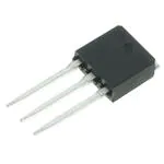
TO-220
G
DS
I2-PAK
G
S
MOSFET Maximum Ratings TC = 25°C unless otherwise noted
Symbol
Parameterr
FDP038AN06A0
FDI038AN06A0
Unit
VDSS
Drain to Source Voltage
60
V
VGS
Gate to Source Voltage
±20
V
Drain Current
ID
Continuous (TC < 151oC, VGS = 10V)
80
A
Continuous (Tamb = 25oC, VGS = 10V, with RθJA = 62oC/W)
17
A
Pulsed
EAS
PD
TJ, TSTG
Single Pulse Avalanche Energy (Note 1)
Figure 4
A
625
mJ
Power dissipation
310
W
Derate above 25oC
2.07
W/oC
-55 to 175
oC
Operating and Storage Temperature
Thermal Characteristics
RθJC
Thermal Resistance, Junction to Case, Max.
RθJA
Thermal Resistance, Junction to Ambient, Max. (Note 2)
©2002 Semiconductor Components Industries, LLC.
September-2017,Rev. 3
0.48
o
C/W
62
o
C/W
Publication Order Number:
FDP038AN06A0/D
FDP038AN06A0 / FDI038AN06A0 — N-Channel PowerTrench® MOSFET
FDP038AN06A0 / FDI038AN06A0
�Device Marking
FDP038AN06A0
Device
FDP038AN06A0
Package
TO-220
Reel Size
Tube
Tape Width
N/A
Quantity
50 units
FDI038AN06A0
FDI038AN06A0
I2-PAK
Tube
N/A
50 units
Electrical Characteristics TC = 25°C unless otherwise noted
Symbol
Parameter
Test Conditions
Min
Typ
Max
Unit
60
-
-
-
V
-
1
-
-
250
µA
VGS = ±20V
-
-
±100
nA
-
4
V
Off Characteristics
BVDSS
Drain to Source Breakdown Voltage
IDSS
Zero Gate Voltage Drain Current
IGSS
Gate to Source Leakage Current
ID = 250µA, VGS = 0V
VDS = 50V
VGS = 0V
TC = 150oC
On Characteristics
VGS(TH)
rDS(ON)
Gate to Source Threshold Voltage
Drain to Source On Resistance
VGS = VDS, ID = 250µA
2
ID = 80A, VGS = 10V
-
0.0035 0.0038
ID = 40A, VGS = 6V
-
0.0049 0.0074
ID = 80A, VGS = 10V,
TJ = 175oC
-
0.0071 0.0078
Ω
Dynamic Characteristics
CISS
Input Capacitance
COSS
Output Capacitance
CRSS
Reverse Transfer Capacitance
Qg(TOT)
Total Gate Charge at 10V
VGS = 0V to 10V
Qg(TH)
Threshold Gate Charge
VGS = 0V to 2V
Qgs
Gate to Source Gate Charge
Qgs2
Gate Charge Threshold to Plateau
Qgd
Gate to Drain “Miller” Charge
Switching Characteristics
VDS = 25V, VGS = 0V,
f = 1MHz
VDD = 30V
ID = 80A
Ig = 1.0mA
-
6400
-
-
1123
-
pF
pF
-
367
-
pF
96
124
nC
-
12
15
nC
-
26
-
nC
-
15
-
nC
-
27
-
nC
(VGS = 10V)
tON
Turn-On Time
-
-
175
ns
td(ON)
Turn-On Delay Time
-
17
-
ns
tr
Rise Time
td(OFF)
Turn-Off Delay Time
tf
tOFF
-
144
-
ns
-
34
-
ns
Fall Time
-
60
-
ns
Turn-Off Time
-
-
115
ns
VDD = 30V, ID = 80A
VGS = 10V, RGS = 2.4Ω
Drain-Source Diode Characteristics
ISD = 80A
-
-
1.25
V
ISD = 40A
-
-
1.0
V
Reverse Recovery Time
ISD = 75A, dISD/dt = 100A/µs
-
-
38
ns
Reverse Recovered Charge
ISD = 75A, dISD/dt = 100A/µs
-
-
39
nC
VSD
Source to Drain Diode Voltage
trr
QRR
Notes:
1: Starting TJ = 25°C, L = 0.255mH, IAS = 70A.
2: Pulse Width = 100s
www.onsemi.com
2
FDP038AN06A0 / FDI038AN06A0 — N-Channel PowerTrench® MOSFET
Package Marking and Ordering Information
�1.2
250
CURRENT LIMITED
BY PACKAGE
ID, DRAIN CURRENT (A)
POWER DISSIPATION MULTIPLIER
1.0
0.8
0.6
0.4
200
150
100
50
0.2
0
0
25
50
75
100
150
125
0
25
175
50
75
TC , CASE TEMPERATURE (oC)
100
125
150
175
o
TC, CASE TEMPERATURE ( C)
Figure 1. Normalized Power Dissipation vs
Ambient Temperature
Figure 2. Maximum Continuous Drain Current vs
Case Temperature
2
DUTY CYCLE - DESCENDING ORDER
0.5
0.2
0.1
0.05
0.02
0.01
ZθJC, NORMALIZED
THERMAL IMPEDANCE
1
PDM
0.1
t1
t2
NOTES:
DUTY FACTOR: D = t1/t2
PEAK TJ = PDM x ZθJC x RθJC + TC
SINGLE PULSE
0.01
10-5
10-4
10-3
10-2
10-1
100
101
t, RECTANGULAR PULSE DURATION (s)
Figure 3. Normalized Maximum Transient Thermal Impedance
3000
1000
IDM, PEAK CURRENT (A)
TC = 25oC
TRANSCONDUCTANCE
MAY LIMIT CURRENT
IN THIS REGION
FOR TEMPERATURES
ABOVE 25oC DERATE PEAK
CURRENT AS FOLLOWS:
175 - TC
I = I25
150
VGS = 10V
100
10
10-5
10-4
10-3
10-2
t, PULSE WIDTH (s)
Figure 4. Peak Current Capability
www.onsemi.com
3
10-1
100
101
FDP038AN06A0 / FDI038AN06A0 — N-Channel PowerTrench® MOSFET
Typical Characteristics TC = 25°C unless otherwise noted
�2000
100
10µs
1000
100
1ms
OPERATION IN THIS
AREA MAY BE
LIMITED BY rDS(ON)
10
10ms
1
DC
SINGLE PULSE
TJ = MAX RATED
TC = 25oC
STARTING TJ = 25oC
IAS, AVALANCHE CURRENT (A)
ID, DRAIN CURRENT (A)
100µs
STARTING TJ = 150oC
10
If R = 0
tAV = (L)(IAS)/(1.3*RATED BVDSS - VDD)
If R ≠ 0
tAV = (L/R)ln[(IAS*R)/(1.3*RATED BVDSS - VDD) +1]
0.1
1
10
1
0.01
100
0.1
1
10
tAV, TIME IN AVALANCHE (ms)
VDS, DRAIN TO SOURCE VOLTAGE (V)
100
NOTE: Refer to ON Semiconductor Application Notes AN7514 and
AN7515
Figure 5. Forward Bias Safe Operating Area
Figure 6. Unclamped Inductive Switching
Capability
160
PULSE DURATION = 80µs
DUTY CYCLE = 0.5% MAX
VDD = 15V
VGS = 20V
ID, DRAIN CURRENT (A)
ID , DRAIN CURRENT (A)
160
120
80
TJ = 175oC
TJ = 25oC
40
120
VGS = 6V
VGS = 5V
80
40
TJ = -55oC
PULSE DURATION = 80µs
DUTY CYCLE = 0.5% MAX
TC = 25oC
0
0
3.0
3.5
4.0
4.5
5.0
5.5
VGS , GATE TO SOURCE VOLTAGE (V)
6
0
Figure 7. Transfer Characteristics
0.5
1.0
VDS , DRAIN TO SOURCE VOLTAGE (V)
1.5
Figure 8. Saturation Characteristics
2.5
6
PULSE DURATION = 80µs
DUTY CYCLE = 0.5% MAX
NORMALIZED DRAIN TO SOURCE
ON RESISTANCE
DRAIN TO SOURCE ON RESISTANCE(mΩ)
VGS = 10V
VGS = 6V
5
4
VGS = 10V
PULSE DURATION = 80µs
DUTY CYCLE = 0.5% MAX
2.0
1.5
1.0
VGS = 10V, ID =80A
3
0
20
40
60
80
0.5
-80
ID, DRAIN CURRENT (A)
Figure 9. Drain to Source On Resistance vs Drain
Current
-40
0
40
80
120
160
TJ, JUNCTION TEMPERATURE (oC)
Figure 10. Normalized Drain to Source On
Resistance vs Junction Temperature
www.onsemi.com
4
200
FDP038AN06A0 / FDI038AN06A0 — N-Channel PowerTrench® MOSFET
Typical Characteristics TC = 25°C unless otherwise noted
�1.4
1.2
VGS = VDS, ID = 250µA
NORMALIZED DRAIN TO SOURCE
BREAKDOWN VOLTAGE
ID = 250µA
NORMALIZED GATE
THRESHOLD VOLTAGE
1.2
1.0
0.8
0.6
0.4
0.2
-80
-40
0
40
80
120
160
1.1
1.0
0.9
200
-80
-40
TJ, JUNCTION TEMPERATURE (oC)
Figure 11. Normalized Gate Threshold Voltage vs
Junction Temperature
10000
80
120
160
200
Figure 12. Normalized Drain to Source
Breakdown Voltage vs Junction Temperature
VGS , GATE TO SOURCE VOLTAGE (V)
C, CAPACITANCE (pF)
CISS = CGS + CGD
CRSS = CGD
VGS = 0V, f = 1MHz
1
VDD = 30V
8
6
4
WAVEFORMS IN
DESCENDING ORDER:
ID = 80A
ID = 40A
2
0
100
0.1
40
10
COSS ≅ CDS + CGD
1000
0
TJ , JUNCTION TEMPERATURE (oC)
10
60
0
VDS , DRAIN TO SOURCE VOLTAGE (V)
Figure 13. Capacitance vs Drain to Source
Voltage
25
50
Qg, GATE CHARGE (nC)
75
100
Figure 14. Gate Charge Waveforms for Constant
Gate Current
www.onsemi.com
5
FDP038AN06A0 / FDI038AN06A0 — N-Channel PowerTrench® MOSFET
Typical Characteristics TC = 25°C unless otherwise noted
�VDS
BVDSS
tP
L
VDS
VARY tP TO OBTAIN
REQUIRED PEAK IAS
IAS
+
RG
VDD
VDD
-
VGS
DUT
tP
IAS
0V
0
0.01Ω
tAV
Figure 15. Unclamped Energy Test Circuit
Figure 16. Unclamped Energy Waveforms
VDS
VDD
Qg(TOT)
VDS
L
VGS
VGS
VGS = 10V
+
Qgs2
VDD
DUT
VGS = 2V
Ig(REF)
0
Qg(TH)
Qgs
Qgd
Ig(REF)
0
Figure 18. Gate Charge Waveforms
Figure 17. Gate Charge Test Circuit
VDS
tON
tOFF
td(ON)
td(OFF)
RL
tr
VDS
tf
90%
90%
+
VGS
VDD
-
10%
0
10%
DUT
90%
RGS
VGS
VGS
0
Figure 19. Switching Time Test Circuit
50%
10%
50%
PULSE WIDTH
Figure 20. Switching Time Waveforms
www.onsemi.com
6
FDP038AN06A0 / FDI038AN06A0 — N-Channel PowerTrench® MOSFET
Test Circuits and Waveforms
�.SUBCKT FDP038AN06A0 2 1 3 ; rev July 04, 2002
Ca 12 8 1.5e-9
Cb 15 14 1.5e-9
Cin 6 8 6.1e-9
LDRAIN
DPLCAP
DRAIN
2
5
10
Dbody 7 5 DbodyMOD
Dbreak 5 11 DbreakMOD
Dplcap 10 5 DplcapMOD
5
51
ESLC
EVTHRES
+ 19 8
+
LGATE
GATE
1
11
+
17
EBREAK 18
-
50
RDRAIN
6
8
ESG
DBREAK
+
RSLC2
Ebreak 11 7 17 18 69.3
Eds 14 8 5 8 1
Egs 13 8 6 8 1
Esg 6 10 6 8 1
Evthres 6 21 19 8 1
Evtemp 20 6 18 22 1
It 8 17 1
RLDRAIN
RSLC1
51
EVTEMP
RGATE + 18 22
9
20
21
16
DBODY
MWEAK
6
MMED
MSTRO
RLGATE
Lgate 1 9 4.81e-9
Ldrain 2 5 1.0e-9
Lsource 3 7 4.63e-9
LSOURCE
CIN
8
7
SOURCE
3
RSOURCE
RLSOURCE
RLgate 1 9 48.1
RLdrain 2 5 10
RLsource 3 7 46.3
Mmed 16 6 8 8 MmedMOD
Mstro 16 6 8 8 MstroMOD
Mweak 16 21 8 8 MweakMOD
S1A
12
S2A
S1B
CA
17
18
RVTEMP
S2B
13
19
CB
6
8
VBAT
5
8
EDS
-
IT
14
+
+
EGS
Rbreak 17 18 RbreakMOD 1
Rdrain 50 16 RdrainMOD 1e-4
Rgate 9 20 1.36
RSLC1 5 51 RSLCMOD 1e-6
RSLC2 5 50 1e3
Rsource 8 7 RsourceMOD 2.8e-3
Rvthres 22 8 RvthresMOD 1
Rvtemp 18 19 RvtempMOD 1
S1a 6 12 13 8 S1AMOD
S1b 13 12 13 8 S1BMOD
S2a 6 15 14 13 S2AMOD
S2b 13 15 14 13 S2BMOD
RBREAK
15
14
13
13
8
-
+
8
22
RVTHRES
Vbat 22 19 DC 1
ESLC 51 50 VALUE={(V(5,51)/ABS(V(5,51)))*(PWR(V(5,51)/(1e-6*250),10))}
.MODEL DbodyMOD D (IS=2.4E-11 N=1.04 RS=1.65e-3 TRS1=2.7e-3 TRS2=2e-7
+ CJO=4.35e-9 M=5.4e-1 TT=1e-9 XTI=3.9)
.MODEL DbreakMOD D (RS=1.5e-1 TRS1=1e-3 TRS2=-8.9e-6)
.MODEL DplcapMOD D (CJO=1.7e-9 IS=1e-30 N=10 M=0.47)
.MODEL MmedMOD NMOS (VTO=3.3 KP=9 IS=1e-30 N=10 TOX=1 L=1u W=1u RG=1.36 T_abs=25)
.MODEL MstroMOD NMOS (VTO=4.00 KP=275 IS=1e-30 N=10 TOX=1 L=1u W=1u T_abs=25)
.MODEL MweakMOD NMOS (VTO=2.72 KP=0.03 IS=1e-30 N=10 TOX=1 L=1u W=1u RG=13.6 RS=0.1 T_abs=25)
.MODEL RbreakMOD RES (TC1=9e-4 TC2=-9e-7)
.MODEL RdrainMOD RES (TC1=4e-2 TC2=3e-4)
.MODEL RSLCMOD RES (TC1=1e-3 TC2=1e-5)
.MODEL RsourceMOD RES (TC1=5e-3 TC2=1e-6)
.MODEL RvthresMOD RES (TC1=-6.7e-3 TC2=-1.5e-5)
.MODEL RvtempMOD RES (TC1=-2.5e-3 TC2=1e-6)
.MODEL S1AMOD VSWITCH (RON=1e-5 ROFF=0.1 VON=-4 VOFF=-1.5)
.MODEL S1BMOD VSWITCH (RON=1e-5 ROFF=0.1 VON=-1.5 VOFF=-4)
.MODEL S2AMOD VSWITCH (RON=1e-5 ROFF=0.1 VON=-1 VOFF=0.5)
.MODEL S2BMOD VSWITCH (RON=1e-5 ROFF=0.1 VON=0.5 VOFF=-1)
.ENDS
Note: For further discussion of the PSPICE model, consult A New PSPICE Sub-Circuit for the Power MOSFET Featuring Global
Temperature Options; IEEE Power Electronics Specialist Conference Records, 1991, written by William J. Hepp and C. Frank
Wheatley.
www.onsemi.com
7
FDP038AN06A0 / FDI038AN06A0 — N-Channel PowerTrench® MOSFET
PSPICE Electrical Model
�rev July 4, 2002
template FDP038AN06A0 n2,n1,n3 = m_temp
electrical n2,n1,n3
number m_temp=25
{
var i iscl
dp..model dbodymod = (isl=2.4e-11,nl=1.04,rs=1.65e-3,trs1=2.7e-3,trs2=2e-7,cjo=4.35e-9,m=5.4e-1,tt=1e-9,xti=3.9)
dp..model dbreakmod = (rs=1.5e-1,trs1=1e-3,trs2=-8.9e-6)
dp..model dplcapmod = (cjo=1.7e-9,isl=10e-30,nl=10,m=0.47)
m..model mmedmod = (type=_n,vto=3.3,kp=9,is=1e-30, tox=1)
m..model mstrongmod = (type=_n,vto=4.00,kp=275,is=1e-30, tox=1)
LDRAIN
m..model mweakmod = (type=_n,vto=2.72,kp=0.03,is=1e-30, tox=1,rs=0.1DP
) LCAP 5
sw_vcsp..model s1amod = (ron=1e-5,roff=0.1,von=-4,voff=-1.5)
10
sw_vcsp..model s1bmod = (ron=1e-5,roff=0.1,von=-1.5,voff=-4)
RLDRAIN
sw_vcsp..model s2amod = (ron=1e-5,roff=0.1,von=-1,voff=0.5)
RSLC1
51
sw_vcsp..model s2bmod = (ron=1e-5,roff=0.1,von=0.5,voff=-1)
RSLC2
c.ca n12 n8 = 1.5e-9
ISCL
c.cb n15 n14 = 1.5e-9
c.cin n6 n8 = 6.1e-9
DBREAK
50
DRAIN
2
-
dp.dbody n7 n5 = model=dbodymod
dp.dbreak n5 n11 = model=dbreakmod
dp.dplcap n10 n5 = model=dplcapmod
spe.ebreak n11 n7 n17 n18 = 69.3
spe.eds n14 n8 n5 n8 = 1
spe.egs n13 n8 n6 n8 = 1
spe.esg n6 n10 n6 n8 = 1
spe.evthres n6 n21 n19 n8 = 1
spe.evtemp n20 n6 n18 n22 = 1
RDRAIN
6
8
ESG
EVTHRES
+ 19 8
+
LGATE
GATE
1
EVTEMP
RGATE + 18 22
9
20
21
EBREAK
+
17
18
-
MMED
MSTRO
CIN
8
LSOURCE
SOURCE
3
7
RSOURCE
RLSOURCE
S1A
i.it n8 n17 = 1
12
S2A
13
8
S1B
CA
RBREAK
15
14
13
17
18
RVTEMP
S2B
13
CB
6
8
EGS
19
VBAT
5
8
EDS
-
IT
14
+
+
res.rlgate n1 n9 = 48.1
res.rldrain n2 n5 = 10
res.rlsource n3 n7 = 46.3
DBODY
MWEAK
6
RLGATE
l.lgate n1 n9 = 4.81e-9
l.ldrain n2 n5 = 1.0e-9
l.lsource n3 n7 = 4.63e-9
11
16
-
+
8
22
RVTHRES
m.mmed n16 n6 n8 n8 = model=mmedmod, temp=m_temp, l=1u, w=1u
m.mstrong n16 n6 n8 n8 = model=mstrongmod, temp=m_temp, l=1u, w=1u
m.mweak n16 n21 n8 n8 = model=mweakmod, temp=m_temp, l=1u, w=1u
res.rbreak n17 n18 = 1, tc1=9e-4,tc2=-9e-7
res.rdrain n50 n16 = 1e-4, tc1=4e-2,tc2=3e-4
res.rgate n9 n20 = 1.36
res.rslc1 n5 n51 = 1e-6, tc1=1e-3,tc2=1e-5
res.rslc2 n5 n50 = 1e3
res.rsource n8 n7 = 2.8e-3, tc1=5e-3,tc2=1e-6
res.rvthres n22 n8 = 1, tc1=-6.7e-3,tc2=-1.5e-5
res.rvtemp n18 n19 = 1, tc1=-2.5e-3,tc2=1e-6
sw_vcsp.s1a n6 n12 n13 n8 = model=s1amod
sw_vcsp.s1b n13 n12 n13 n8 = model=s1bmod
sw_vcsp.s2a n6 n15 n14 n13 = model=s2amod
sw_vcsp.s2b n13 n15 n14 n13 = model=s2bmod
v.vbat n22 n19 = dc=1
equations {
i (n51->n50) +=iscl
iscl: v(n51,n50) = ((v(n5,n51)/(1e-9+abs(v(n5,n51))))*((abs(v(n5,n51)*1e6/250))** 10))
}
www.onsemi.com
8
FDP038AN06A0 / FDI038AN06A0 — N-Channel PowerTrench® MOSFET
SABER Electrical Model
�th
REV 23 July 4, 2002
JUNCTION
FDP038AN06A0T
CTHERM1 TH 6 6.45e-3
CTHERM2 6 5 3e-2
CTHERM3 5 4 1.4e-2
CTHERM4 4 3 1.65e-2
CTHERM5 3 2 4.85e-2
CTHERM6 2 TL 1e-1
RTHERM1
CTHERM1
6
RTHERM1 TH 6 3.24e-3
RTHERM2 6 5 8.08e-3
RTHERM3 5 4 2.28e-2
RTHERM4 4 3 1e-1
RTHERM5 3 2 1.1e-1
RTHERM6 2 TL 1.4e-1
RTHERM2
CTHERM2
5
SABER Thermal Model
RTHERM3
SABER thermal model FDP035AN06A0T
template thermal_model th tl
thermal_c th, tl
{
ctherm.ctherm1 th 6 =6.45e-3
ctherm.ctherm2 6 5 =3e-2
ctherm.ctherm3 5 4 =1.4e-2
ctherm.ctherm4 4 3 =1.65e-2
ctherm.ctherm5 3 2 =4.85e-2
ctherm.ctherm6 2 tl =1e-1
CTHERM3
4
RTHERM4
CTHERM4
3
rtherm.rtherm1 th 6 =3.24e-3
rtherm.rtherm2 6 5 =8.08e-3
rtherm.rtherm3 5 4 =2.28e-2
rtherm.rtherm4 4 3 =1e-1
rtherm.rtherm5 3 2 =1.1e-1
rtherm.rtherm6 2 tl=1.4e-1
}
RTHERM5
CTHERM5
2
CTHERM6
RTHERM6
tl
www.onsemi.com
9
CASE
FDP038AN06A0 / FDI038AN06A0 — N-Channel PowerTrench® MOSFET
SPICE Thermal Model
�FDP038AN06A0 / FDI038AN06A0 — N-Channel PowerTrench® MOSFET
Mechanical Dimensions
TO-220 3L
Figure 21. TO-220, Molded, 3Lead, Jedec Variation AB
Package drawings are provided as a service to customers considering ON Semiconductor components. Drawings may change in
any manner without notice. Please note the revision and/or date on the drawing and contact a ON Semiconductor representative to
verify or obtain the most recent revision. Package specifications do not expand the terms of ON Semiconductor’s worldwide terms
and conditions, specif-ically the warranty therein, which covers ON Semiconductor products.
Dimension in Millimeters
www.onsemi.com
10
�FDP038AN06A0 / FDI038AN06A0 — N-Channel PowerTrench® MOSFET
Mechanical Dimensions
TO-262 3L (I2PAK)
Figure 22. 3LD, TO262, Jedec Variation AA (I2PAK)
Package drawings are provided as a service to customers considering ON Semiconductor components. Drawings may change in
any manner without notice. Please note the revision and/or date on the drawing and contact a ON Semiconductor representative to
verify or obtain the most recent revision. Package specifications do not expand the terms of ON Semiconductor’s worldwide terms
and conditions, specif-ically the warranty therein, which covers ON Semiconductor products.
Dimension in Millimeters
www.onsemi.com
11
�ON Semiconductor and
are trademarks of Semiconductor Components Industries, LLC dba ON Semiconductor or its subsidiaries in the United States and/or other countries.
ON Semiconductor owns the rights to a number of patents, trademarks, copyrights, trade secrets, and other intellectual property. A listing of ON Semiconductor’s product/patent
coverage may be accessed at www.onsemi.com/site/pdf/Patent−Marking.pdf. ON Semiconductor reserves the right to make changes without further notice to any products herein.
ON Semiconductor makes no warranty, representation or guarantee regarding the suitability of its products for any particular purpose, nor does ON Semiconductor assume any liability
arising out of the application or use of any product or circuit, and specifically disclaims any and all liability, including without limitation special, consequential or incidental damages.
Buyer is responsible for its products and applications using ON Semiconductor products, including compliance with all laws, regulations and safety requirements or standards,
regardless of any support or applications information provided by ON Semiconductor. “Typical” parameters which may be provided in ON Semiconductor data sheets and/or
specifications can and do vary in different applications and actual performance may vary over time. All operating parameters, including “Typicals” must be validated for each customer
application by customer’s technical experts. ON Semiconductor does not convey any license under its patent rights nor the rights of others. ON Semiconductor products are not
designed, intended, or authorized for use as a critical component in life support systems or any FDA Class 3 medical devices or medical devices with a same or similar classification
in a foreign jurisdiction or any devices intended for implantation in the human body. Should Buyer purchase or use ON Semiconductor products for any such unintended or unauthorized
application, Buyer shall indemnify and hold ON Semiconductor and its officers, employees, subsidiaries, affiliates, and distributors harmless against all claims, costs, damages, and
expenses, and reasonable attorney fees arising out of, directly or indirectly, any claim of personal injury or death associated with such unintended or unauthorized use, even if such
claim alleges that ON Semiconductor was negligent regarding the design or manufacture of the part. ON Semiconductor is an Equal Opportunity/Affirmative Action Employer. This
literature is subject to all applicable copyright laws and is not for resale in any manner.
PUBLICATION ORDERING INFORMATION
LITERATURE FULFILLMENT:
Literature Distribution Center for ON Semiconductor
19521 E. 32nd Pkwy, Aurora, Colorado 80011 USA
Phone: 303−675−2175 or 800−344−3860 Toll Free USA/Canada
Fax: 303−675−2176 or 800−344−3867 Toll Free USA/Canada
Email: orderlit@onsemi.com
❖
© Semiconductor Components Industries, LLC
N. American Technical Support: 800−282−9855 Toll Free
USA/Canada
Europe, Middle East and Africa Technical Support:
Phone: 421 33 790 2910
Japan Customer Focus Center
Phone: 81−3−5817−1050
ON Semiconductor Website: www.onsemi.com
Order Literature: http://www.onsemi.com/orderlit
For additional information, please contact your local
Sales Representative
www.onsemi.com
�


 工商网监
湘ICP备2023018690号
工商网监
湘ICP备2023018690号
