Is Now Part of
To learn more about ON Semiconductor, please visit our website at
www.onsemi.com
Please note: As part of the Fairchild Semiconductor integration, some of the Fairchild orderable part numbers
will need to change in order to meet ON Semiconductor’s system requirements. Since the ON Semiconductor
product management systems do not have the ability to manage part nomenclature that utilizes an underscore
(_), the underscore (_) in the Fairchild part numbers will be changed to a dash (-). This document may contain
device numbers with an underscore (_). Please check the ON Semiconductor website to verify the updated
device numbers. The most current and up-to-date ordering information can be found at www.onsemi.com. Please
email any questions regarding the system integration to Fairchild_questions@onsemi.com.
ON Semiconductor and the ON Semiconductor logo are trademarks of Semiconductor Components Industries, LLC dba ON Semiconductor or its subsidiaries in the United States and/or other countries. ON Semiconductor owns the rights to a number
of patents, trademarks, copyrights, trade secrets, and other intellectual property. A listing of ON Semiconductor’s product/patent coverage may be accessed at www.onsemi.com/site/pdf/Patent-Marking.pdf. ON Semiconductor reserves the right
to make changes without further notice to any products herein. ON Semiconductor makes no warranty, representation or guarantee regarding the suitability of its products for any particular purpose, nor does ON Semiconductor assume any liability
arising out of the application or use of any product or circuit, and specifically disclaims any and all liability, including without limitation special, consequential or incidental damages. Buyer is responsible for its products and applications using ON
Semiconductor products, including compliance with all laws, regulations and safety requirements or standards, regardless of any support or applications information provided by ON Semiconductor. “Typical” parameters which may be provided in ON
Semiconductor data sheets and/or specifications can and do vary in different applications and actual performance may vary over time. All operating parameters, including “Typicals” must be validated for each customer application by customer’s
technical experts. ON Semiconductor does not convey any license under its patent rights nor the rights of others. ON Semiconductor products are not designed, intended, or authorized for use as a critical component in life support systems or any FDA
Class 3 medical devices or medical devices with a same or similar classification in a foreign jurisdiction or any devices intended for implantation in the human body. Should Buyer purchase or use ON Semiconductor products for any such unintended
or unauthorized application, Buyer shall indemnify and hold ON Semiconductor and its officers, employees, subsidiaries, affiliates, and distributors harmless against all claims, costs, damages, and expenses, and reasonable attorney fees arising out
of, directly or indirectly, any claim of personal injury or death associated with such unintended or unauthorized use, even if such claim alleges that ON Semiconductor was negligent regarding the design or manufacture of the part. ON Semiconductor
is an Equal Opportunity/Affirmative Action Employer. This literature is subject to all applicable copyright laws and is not for resale in any manner.
�FDMS030N06B
N 沟道 PowerTrench® MOSFET
60 V, 100 A, 3 m
特性
说明
• RDS(on) = 2.4 m (典型值) @ VGS = 10 V, ID = 50 A
此 N 沟道 MOSFET 采用飞兆半导体先进的 Power Trench® 工
艺生产,这一先进工艺是专为最大限度地降低导通电阻并保持卓
越开关性能而定制的。
• 低 RDS(on) 和高效的先进硅封装组合
• 快速开关速度
应用
• 100% 经过 UIL 测试
• 符合 RoHS 标准
• 用于 ATX/ 服务器 / 电信 PSU 的同步整流
• 电池保护电路
• 电机驱动和不间断电源
• 可再生系统
底
顶
S
D
D
D
引脚 1
S
S
G
D
D
5
4
G
D
6
3
S
D
7
2
S
D
8
1
S
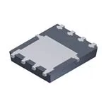
Power 56
MOSFET 最大额定值 TC = 25°C 除非另有说明。
符号
参数
VDSS
漏极-源极电压
VGSS
栅极-源极电压
ID
漏极电流
IDM
漏极电流
EAS
单脉冲雪崩能量
PD
功耗
TJ,, TSTG
工作和存储温度范围
FDMS030N06B
60
单位
V
±20
V
- 连续 (TC = 25°C)
(说明 1)
100
- 连续 (TA = 25°C)
(说明 2a)
22.1
(说明 3)
400
A
(说明 4)
248
mJ
- 脉冲
(TC = 25°C)
(TA = 25°C)
(说明 2a)
A
104
W
2.5
W
-55 至 +150
°C
FDMS030N06B
单位
热性能
符号
参数
RJC
结至外壳热阻最大值
RJA
结至环境热阻最大值
©2010 飞兆半导体公司
FDMS030N06B Rev. C1
1.2
(说明 2a)
1
50
°C/W
www.fairchildsemi.com
FDMS030N06BN 沟道 PowerTrench® MOSFET
2014 年 1 月
�器件标识
FDMS030N06B
器件
FDMS030N06B
封装
Power 56
卷尺寸
13 ”
带宽
12 mm
数量
3000 个
电气特性 TC = 25°C 除非另有说明。
符号
参数
测试条件
最小值
典型值
最大值
单位
60
-
-
V
-
0.03
-
V/°C
关断特性
BVDSS
BVDSS
/ TJ
IDSS
漏极-源极击穿电压
ID = 250 A, VGS = 0 V
击穿电压温度系数
ID = 250 A,推荐选用 25°C
零栅极电压漏极电流
VDS = 48 V, VGS = 0 V
-
-
1
A
IGSS
栅极 - 体漏电流
VGS = ±20 V, VDS = 0 V
-
-
±100
nA
VGS(th)
RDS(on)
栅极阈值电压
VGS = VDS, ID = 250 A
2.5
3.3
4.5
V
漏极至源极静态导通电阻
-
2.4
3.0
m
gFS
正向跨导
VGS = 10 V, ID = 50 A
VDS = 10 V, ID = 50 A
-
119
-
S
导通特性
动态特性
Ciss
输入电容
Coss
输出电容
Crss
反向传输电容
Coss(er)
能量相关输出电容
Qg(tot)
10 V 的栅极电荷总量
Qgs
栅极 - 源极栅极电荷
Qgd
栅极 - 漏极 “ 米勒 ” 电荷
VDS = 30 V, VGS = 0 V
f = 1 MHz
-
5685
7560
pF
-
1720
2290
pF
-
59
-
pF
VDS = 30 V, VGS = 0 V
-
2504
-
pF
-
75
-
nC
-
30
-
nC
-
14
-
nC
-
5.4
-
V
VDS = 30 V, ID = 50 A
VGS = 0 V to 10 V
Vplateau
栅极平台电压
Qsync
总栅极电荷同步
VDS = 0 V, ID = 50 A
-
66.2
-
nC
Qoss
输出电荷
VDS = 30 V, VGS = 0 V
-
174
-
nC
ESR
等效串联电阻
f = 1 MHz
-
1.05
-
-
39
88
ns
-
20
50
ns
-
52
114
ns
-
16
42
ns
(说明 5)
开关特性
td(on)
导通延迟时间
tr
开通上升时间
td(off)
关断延迟时间
tf
关断下降时间
VDD = 30 V, ID = 50 A
VGS = 10 V, RG = 4.7
(说明 5)
漏极 - 源极二极管特性
IS
漏极 - 源极二极管最大正向连续电流
-
-
100
A
ISM
漏极 - 源极二极管最大正向脉冲电流
-
-
400
A
VSD
漏极 - 源极二极管正向电压
VGS = 0 V, ISD = 50 A
-
-
1.25
V
trr
反向恢复时间
-
71
-
ns
Qrr
反向恢复电荷
VGS = 0 V, ISD = 50 A
dIF/dt = 100 A/s
-
85
-
nC
注意:
1. 硅限制 ID 额定值 = 147 A。
2. RJA 取决于安装在 FR-4 材质 1.5 x 1.5 in. 电路板上 1 in2 焊盘和 2 盎司铜焊盘上的器件。 RJC 通过设计保证,而 RCA 取决于用户的电路板设计。
b. 125 °C/W,安装于
最小尺寸的 2 盎司焊盘。
a. 50 °C/W,安装于
1 in2 2 盎司焊盘。
3. 重复额定值:脉冲宽度受限于最大结温。
4. L = 0.3 mH, IAS = 40.7 A, VDD = 50 V, VGS = 10 V,开始 TJ = 25°C。
5. 本质上独立于工作温度的典型特性。
©2010 飞兆半导体公司
FDMS030N06B Rev. C1
2
www.fairchildsemi.com
FDMS030N06BN 沟道 PowerTrench® MOSFET
封装标识与定购信息
�图 1. 导通区域特性
图 2. 传输特性
200
500
*Notes:
1. VDS = 10V
2. 250s Pulse Test
10
RDS(ON) [m],
Drain-Source On-Resistance
1
0.05
ID, Drain Current[A]
100
VGS = 15.0V
10.0V
8.0V
7.0V
6.5V
*Notes:
6.0V
1. 250s Pulse Test
5.5V
o
2. TC = 25 C
5.0V
0.1
1
VDS, Drain-Source Voltage[V]
o
o
25 C
150 C
o
-55 C
10
1
3
3
4
5
6
VGS, Gate-Source Voltage[V]
图 3. 导通电阻变化与漏极电流和栅极电压
图 4. 体二极管正向电压变化与源极电流和温度
500
3.0
VGS = 10V
2.5
2.0
VGS = 20V
1.5
100
o
150 C
o
25 C
10
*Notes:
1. VGS = 0V
o
1.0
2. 250s Pulse Test
*Note: TC = 25 C
0
50
100
150
ID, Drain Current [A]
1
0.2
200
图 5. 电容特性
VGS, Gate-Source Voltage [V]
Coss
1000
10
0.1
1.4
10
Ciss
100
0.4
0.6
0.8
1.0
1.2
VSD, Body Diode Forward Voltage [V]
图 6. 栅极电荷
10000
Capacitances [pF]
7
3.5
IS, Reverse Drain Current [A]
ID, Drain Current[A]
100
*Note:
1. VGS = 0V
2. f = 1MHz
Ciss = Cgs + Cgd (Cds = shorted)
Coss = Cds + Cgd
Crss = Cgd
©2010 飞兆半导体公司
FDMS030N06B Rev. C1
1
10
VDS, Drain-Source Voltage [V]
VDS = 12V
VDS = 30V
VDS = 48V
8
6
4
2
Crss
*Note: ID = 50A
0
60
3
0
15
30
45
60
75
Qg, Total Gate Charge [nC]
90
www.fairchildsemi.com
FDMS030N06BN 沟道 PowerTrench® MOSFET
典型性能特征
�图 8. 导通电阻变化与温度
1.06
1.8
1.04
1.6
RDS(on), [Normalized]
Drain-Source On-Resistance
BVDSS, [Normalized]
Drain-Source Breakdown Voltage
图 7. 击穿电压变化与温度
1.02
1.00
0.98
*Notes:
1. VGS = 0V
2. ID = 250A
0.96
0.94
-80
-40
0
40
80 o 120
TJ, Junction Temperature [ C]
1.4
1.2
1.0
0.6
-80
160
图 9. 最大安全工作区
*Notes:
1. VGS = 10V
2. ID = 50A
0.8
-40
0
40
80
120
o
TJ, Junction Temperature [ C]
160
图 10. 最大漏极电流与外壳温度
1000
150
100
120
ID, Drain Current [A]
ID, Drain Current [A]
VGS= 10V
1ms
10
10ms
100ms
Operation in This Area
is Limited by R DS(on)
1
DC
*Notes:
o
0.1
90
60
30
1. Ta = 25 C
o
0.01
0.01
2. TJ = 150 C
3. Single Pulse
0.1
1
10
VDS, Drain-Source Voltage [V]
o
RJC= 1.2 C/W
0
25
100
图 11. 输出电容 (Eoss) 与漏极 - 源极电压
150
图 12. 非箝位电感开关能力
3.0
IAS, Avalanche Current [A]
100
2.5
EOSS, [J]
50
75
100
125
o
TC, Case Temperature [ C]
2.0
1.5
1.0
o
TJ = 25 C
10
o
TJ = 125 C
0.5
0
0
©2010 飞兆半导体公司
FDMS030N06B Rev. C1
10
20
30
40
50
VDS, Drain to Source Voltage [V]
1
0.001
60
4
0.01
0.1
1
10
100
tAV, Time In Avalanche [ms]
1,000
www.fairchildsemi.com
FDMS030N06BN 沟道 PowerTrench® MOSFET
典型性能特征 (接上页)
�FDMS030N06BN 沟道 PowerTrench® MOSFET
典型性能特征 (接上页)
图 13. 瞬态热响应曲线
2
1
热响应,ZJA(t)
(标准化)
Impedance [ZJA]
Normalized Thermal
0.5
0.2
0.1
0.1
PDM
0.05
t1
0.02
0.01
0.01
t2
*Notes:
Single pulse
o
0.001
1E-3
0.01
1. ZJA(t) = 125 C/W Max.
2. Duty Factor, D= t1/t2
3. TJM - TC = PDM * ZJC(t)
0.1
1
10
100
1000
Pulse
[sec]
t1,Rectangular
矩形脉冲持续时间
[ 秒Duration
]
©2010 飞兆半导体公司
FDMS030N06B Rev. C1
5
www.fairchildsemi.com
�FDMS030N06BN 沟道 PowerTrench® MOSFET
图 14. 栅极电荷测试电路与波形
IG = 常量
图 15. 阻性开关测试电路与波形
VDS
RG
VGS
10V
RL
VDS
90%
VDD
VGS
VGS
DUT
10%
td(on)
tr
t on
td(off)
tf
t off
图 16. 非箝位电感开关测试电路与波形
VGS
©2010 飞兆半导体公司
FDMS030N06B Rev. C1
6
www.fairchildsemi.com
�FDMS030N06BN 沟道 PowerTrench® MOSFET
图 17. 二极管恢复 dv/dt 峰值测试电路与波形
DUT
+
VDS
_
I SD
L
Driver
RG
VGS
VGS
( Driver )
Same Type
as DUT
VDD
• dv/dt controlled by RG
• ISD controlled by pulse period
Gate Pulse Width
D = -------------------------Gate Pulse Period
10V
IFM , Body Diode Forward Current
I SD
( DUT )
di/dt
IRM
Body Diode Reverse Current
VDS
( DUT )
Body Diode Recovery dv/dt
VSD
VDD
Body Diode
Forward Voltage Drop
©2010 飞兆半导体公司
FDMS030N06B Rev. C1
7
www.fairchildsemi.com
�VCC
Driver
VGS
( Driver)
VGS
(DUT)
VDD
VRG
RG
10V
t
DUT
Qsync
VGS
©2010 飞兆半导体公司
FDMS030N06B Rev. C1
t
8
1
VR t dt
RG G
www.fairchildsemi.com
FDMS030N06BN 沟道 PowerTrench® MOSFET
图 18. 总栅极电荷 Qsync 测试电路与波形
�PQFN8 5X6, 1.27P
CASE 483AE
ISSUE A
5.10
PKG
CL
8
5.10
3.91
A
SEE
DETAIL B
B
5
1.27
8
7
6
5
0.77
4.52
PKG CL
5.85
5.65
6.15
3.75
6.61
KEEP OUT
AREA
1.27
1
4
1
TOP VIEW
2
3
4
0.61
1.27
3.81
OPTIONAL DRAFT
ANGLE MAY APPEAR
ON FOUR SIDES
OF THE PACKAGE
SEE
DETAIL C
5.00
4.80
LAND PATTERN
RECOMMENDATION
0.35
0.15
0.10 C
0.05
0.00
SIDE VIEW
8X
0.08 C
5.20
4.80
1.10
0.90
3.81
0.35
0.15
DETAIL C
SCALE: 2:1
1.27
0.51 (8X)
0.31
(0.34)
0.10
1
2
3
C A B
4
0.76
0.51
(0.52)
6.25
5.90
3.48+0.30
-0.10
(0.50)
(0.30)
(2X)
8
0.20+0.10
-0.15 (8X)
7
6
3.96
3.61
BOTTOM VIEW
0.30
0.05
5
C
SEATING
PLANE
DETAIL B
SCALE: 2:1
NOTES: UNLESS OTHERWISE SPECIFIED
A. PACKAGE STANDARD REFERENCE: JEDEC MO-240,
ISSUE A, VAR. AA,.
B. DIMENSIONS DO NOT INCLUDE BURRS OR MOLD FLASH.
MOLD FLASH OR BURRS DOES NOT EXCEED 0.10MM.
C. ALL DIMENSIONS ARE IN MILLIMETERS.
D. DIMENSIONING AND TOLERANCING PER ASME Y14.5M-2009.
E. IT IS RECOMMENDED TO HAVE NO TRACES OR
VIAS WITHIN THE KEEP OUT AREA.
�ON Semiconductor and
are trademarks of Semiconductor Components Industries, LLC dba ON Semiconductor or its subsidiaries in the United States and/or other countries.
ON Semiconductor owns the rights to a number of patents, trademarks, copyrights, trade secrets, and other intellectual property. A listing of ON Semiconductor’s product/patent
coverage may be accessed at www.onsemi.com/site/pdf/Patent−Marking.pdf. ON Semiconductor reserves the right to make changes without further notice to any products herein.
ON Semiconductor makes no warranty, representation or guarantee regarding the suitability of its products for any particular purpose, nor does ON Semiconductor assume any liability
arising out of the application or use of any product or circuit, and specifically disclaims any and all liability, including without limitation special, consequential or incidental damages.
Buyer is responsible for its products and applications using ON Semiconductor products, including compliance with all laws, regulations and safety requirements or standards,
regardless of any support or applications information provided by ON Semiconductor. “Typical” parameters which may be provided in ON Semiconductor data sheets and/or
specifications can and do vary in different applications and actual performance may vary over time. All operating parameters, including “Typicals” must be validated for each customer
application by customer’s technical experts. ON Semiconductor does not convey any license under its patent rights nor the rights of others. ON Semiconductor products are not
designed, intended, or authorized for use as a critical component in life support systems or any FDA Class 3 medical devices or medical devices with a same or similar classification
in a foreign jurisdiction or any devices intended for implantation in the human body. Should Buyer purchase or use ON Semiconductor products for any such unintended or unauthorized
application, Buyer shall indemnify and hold ON Semiconductor and its officers, employees, subsidiaries, affiliates, and distributors harmless against all claims, costs, damages, and
expenses, and reasonable attorney fees arising out of, directly or indirectly, any claim of personal injury or death associated with such unintended or unauthorized use, even if such
claim alleges that ON Semiconductor was negligent regarding the design or manufacture of the part. ON Semiconductor is an Equal Opportunity/Affirmative Action Employer. This
literature is subject to all applicable copyright laws and is not for resale in any manner.
PUBLICATION ORDERING INFORMATION
LITERATURE FULFILLMENT:
Literature Distribution Center for ON Semiconductor
19521 E. 32nd Pkwy, Aurora, Colorado 80011 USA
Phone: 303−675−2175 or 800−344−3860 Toll Free USA/Canada
Fax: 303−675−2176 or 800−344−3867 Toll Free USA/Canada
Email: orderlit@onsemi.com
© Semiconductor Components Industries, LLC
N. American Technical Support: 800−282−9855 Toll Free
USA/Canada
Europe, Middle East and Africa Technical Support:
Phone: 421 33 790 2910
Japan Customer Focus Center
Phone: 81−3−5817−1050
www.onsemi.com
1
ON Semiconductor Website: www.onsemi.com
Order Literature: http://www.onsemi.com/orderlit
For additional information, please contact your local
Sales Representative
www.onsemi.com
�


 工商网监
湘ICP备2023018690号
工商网监
湘ICP备2023018690号
