Is Now Part of
To learn more about ON Semiconductor, please visit our website at
www.onsemi.com
Please note: As part of the Fairchild Semiconductor integration, some of the Fairchild orderable part numbers
will need to change in order to meet ON Semiconductor’s system requirements. Since the ON Semiconductor
product management systems do not have the ability to manage part nomenclature that utilizes an underscore
(_), the underscore (_) in the Fairchild part numbers will be changed to a dash (-). This document may contain
device numbers with an underscore (_). Please check the ON Semiconductor website to verify the updated
device numbers. The most current and up-to-date ordering information can be found at www.onsemi.com. Please
email any questions regarding the system integration to Fairchild_questions@onsemi.com.
ON Semiconductor and the ON Semiconductor logo are trademarks of Semiconductor Components Industries, LLC dba ON Semiconductor or its subsidiaries in the United States and/or other countries. ON Semiconductor owns the rights to a number
of patents, trademarks, copyrights, trade secrets, and other intellectual property. A listing of ON Semiconductor’s product/patent coverage may be accessed at www.onsemi.com/site/pdf/Patent-Marking.pdf. ON Semiconductor reserves the right
to make changes without further notice to any products herein. ON Semiconductor makes no warranty, representation or guarantee regarding the suitability of its products for any particular purpose, nor does ON Semiconductor assume any liability
arising out of the application or use of any product or circuit, and specifically disclaims any and all liability, including without limitation special, consequential or incidental damages. Buyer is responsible for its products and applications using ON
Semiconductor products, including compliance with all laws, regulations and safety requirements or standards, regardless of any support or applications information provided by ON Semiconductor. “Typical” parameters which may be provided in ON
Semiconductor data sheets and/or specifications can and do vary in different applications and actual performance may vary over time. All operating parameters, including “Typicals” must be validated for each customer application by customer’s
technical experts. ON Semiconductor does not convey any license under its patent rights nor the rights of others. ON Semiconductor products are not designed, intended, or authorized for use as a critical component in life support systems or any FDA
Class 3 medical devices or medical devices with a same or similar classification in a foreign jurisdiction or any devices intended for implantation in the human body. Should Buyer purchase or use ON Semiconductor products for any such unintended
or unauthorized application, Buyer shall indemnify and hold ON Semiconductor and its officers, employees, subsidiaries, affiliates, and distributors harmless against all claims, costs, damages, and expenses, and reasonable attorney fees arising out
of, directly or indirectly, any claim of personal injury or death associated with such unintended or unauthorized use, even if such claim alleges that ON Semiconductor was negligent regarding the design or manufacture of the part. ON Semiconductor
is an Equal Opportunity/Affirmative Action Employer. This literature is subject to all applicable copyright laws and is not for resale in any manner.
�FSA2258 Low-Voltage, Dual-SPDT
(0.8) Analog Switch with 16kV ESD
Features
Description
The FSA2258 is a high-performance, dual, Single Pole
Double Throw (SPDT) analog switch that features low
RON of 0.8 (typical) at 3.0V VCC. The FSA2258
operates over a wide VCC range of 1.65V to 4.3V and is
designed for break-before-make operation. The select
input is TTL-level compatible.
0.8Ω Typical On Resistance (RON) for +3.0V Supply
0.40Ω Maximum RON Flatness for +3.0V Supply
-3db Bandwidth: > 50MHz
Low ICCT Current Over an Expanded Control Input
Range
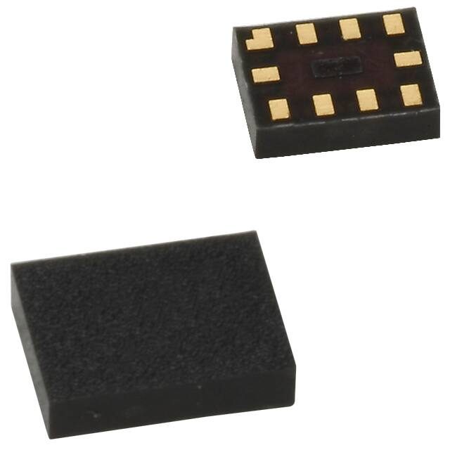
Packaged in 10-Lead MicroPak™ (1.6 x 2.1mm)
Power-Off Protection on Common Ports
Broad VCC Operating Range: 1.65V to 4.30V
HBM JEDEC: JESD22-A114
- I/O to GND: 9kV
- Power to GND: 16kV
IMPORTANT NOTE:
For
additional
information,
analogswitch@fairchildsemi.com.
Applications
The FSA2258 features very low quiescent current even
when the control voltage is lower than the VCC supply.
This feature suits mobile handset applications by
allowing direct interface with baseband processor
general-purpose I/Os with minimal battery consumption.
please
contact
Cell Phone, PDA, Digital Camera, and Notebook
LCD Monitor, TV, and Set-Top Box
Ordering Information
Part Number
Top Mark
Operating
Temperature Range
Package
FSA2258L10X
JS
-40 to +85°C
10-Lead MicroPak™ 1.6 x 2.1mm, JEDEC MO-255B
Analog Symbol
1B0
1B1
1A
S1
2B0
2B1
Figure 1.
© 2008 Fairchild Semiconductor Corporation
FSA2258 • Rev. 1.0.5
2A
S2
FSA2258
www.fairchildsemi.com
FSA2258 — Low-Voltage Dual-SPDT (0.8) Analog Switch with 16kV ESD
February 2012
�FSA2258 — Low-Voltage, Dual-SPDT (0.8) Analog Switch with 16kV ESD
Pin Configuration
Vcc
10
1B0
1
9
1A
1B1
2
8
S1
2B0
3
7
S2
2B1
4
6
2A
5
GND
Figure 2. 10-Lead MicroPak™ (Top-Through View)
Pin Descriptions
Pin #
Name
Description
1
1B0
Data Ports
2
1B1
Data Ports
3
2B0
Data Ports
4
2B1
5
GND
Data Ports
6
2A
Data Ports
7
S2
Switch Select Pins
8
S1
Switch Select Pins
9
1A
Data Ports
10
VCC
Supply Voltage
Ground
Truth Table
Control Input, Sn
Function
LOW Logic Level
nB0 connected to nA
HIGH Logic Level
nB1 connected to nA
© 2008 Fairchild Semiconductor Corporation
FSA2258 • Rev. 1.0.5
www.fairchildsemi.com
2
�Stresses exceeding the absolute maximum ratings may damage the device. The device may not function or be
operable above the recommended operating conditions and stressing the parts to these levels is not recommended.
In addition, extended exposure to stresses above the recommended operating conditions may affect device reliability.
The absolute maximum ratings are stress ratings only.
Symbol Parameter
VCC
VSW
Supply Voltage
(1)
Switch I/O Voltage
(1)
Min.
Max.
Units
-0.5
5.5
V
1B0, 1B1, 2B0, 2B1,
1A, 2A Pins
-0.5
VCC + 0.3
V
S1, S2
-0.5
VIN
Control Input Voltage
5.5
V
IIK
Input Clamp Diode Current
-50
mA
ISW
Switch I/O Current (Continuous)
350
mA
Peak Switch Current (Pulsed at 1ms Duration, 50
MHz
Figure 9
THD+N
Total
Harmonic
Distortion +
Noise(6)
f=20Hz to 20kHz,
1.65 to 4.30
RL=32,
VIN=2VPP
.06
%
Figure 15
Unit
Figure
Q
Note:
6. Guaranteed by characterization, not production tested
Capacitance
All capacitance specifications are guaranteed by characterization and are not production tested.
Symbol
Parameter
Conditions
VCC (V)
TA=+25ºC
Min.
Typ.
Max.
CIN
Control Pin Input Capacitance
f=1MHz
0
1.5
pF
Figure 13
COFF
B Port Off Capacitance
f=1MHz
3.3
30
pF
Figure 13
CON
A Port On Capacitance
f=1MHz
3.3
50
pF
Figure 14
© 2008 Fairchild Semiconductor Corporation
FSA2258 • Rev. 1.0.5
www.fairchildsemi.com
5
FSA2258 — Low-Voltage, Dual-SPDT (0.8) Analog Switch with 16kV ESD
AC Electrical Characteristics
�VON
I A(OFF)
NC
nBn
A
nA
V IN
V IN
GND
I ON
Select
V Sel =
R ON = VON / ION
Figure 3.
Select
VSel =
GND
0 or Vcc
**Each switch port is tested separately.
On Resistance
Figure 4.
Off Leakage (Ports Tested Separately)
nBn
I A(ON)
NC
GND
V IN
Select
Figure 5.
nA
V IN
A
VSel =
GND
0 orVcc
RS
CL
RL
V OUT
GND
GND
V Sel
0 or Vcc
GND
On Leakage
Figure 6.
tRISE = 2.5ns
Test Circuit Load
tFALL = 2.5ns
VCC
Input - VSel
10%
GND
VOH
Output - VOUT
VOL
Figure 7.
© 2008 Fairchild Semiconductor Corporation
FSA2258 • Rev. 1.0.5
90%
90%
VCC /2
VCC /2
90%
tON
10%
90%
tOFF
Turn-On / Turn-Off Waveforms
www.fairchildsemi.com
6
FSA2258 — Low-Voltage, Dual-SPDT (0.8) Analog Switch with 16kV ESD
Test Diagrams
�t RISE = 2.5ns
nB n
nA
V cc
V IN
GN D
VOUT
CL
V IN
R
L
10%
0V
GN D
GND
90%
V cc /2
Input - VSel
V OUT
RS
0.9*V out
0.9*V out
V Sel
GN D
tBBM
RL and CL are functions of the application
environment (50, 75, or 100 ).
CL includes test fixture and stray capacitance.
Figure 8.
Break-Before-Make Interval Timing
Network Analyzer
RS
GND
V IN
VS
GND
VSel
GND
VOU T
GND
RT
RL and CL are functions of the application
environment (50, 75, or 100 ).
L
CL includes
test fixture and stray capacitance.
Figure 9.
GND
Bandwidth
Network Analyzer
RS
VSel
VS
GND
RT
GND
GND
VOUT
GND
GND
RS and RT are functions of the application
environment (50, 75, or 100 ).
RT
GND
Off-Isolation
= 20 Log (VOUT / V IN )
Figure 10.
© 2008 Fairchild Semiconductor Corporation
FSA2258 • Rev. 1.0.5
Channel Off Isolation
www.fairchildsemi.com
7
FSA2258 — Low-Voltage, Dual-SPDT (0.8) Analog Switch with 16kV ESD
Test Diagrams (Continued)
�Network Analyzer
RS
VIN
GND
VS
GND
VSel
GND
GND
RT
V OUT
RT
GND
GND
RS and RT are functions of the application
CROSSTALK = 20 Log (VOUT / VIN )
environment (50, 75, or 100 ).
Figure 11.
Adjacent Channel Crosstalk
Generator
VCC
B
RS
VS
VIN
Input – VSEL
mA
CL
GND
nSn
Off
On
Off
0V
VOUT
VOUT
GND
VOUT
VSEL
CL includes test fixture and stray capacitance
GND
Figure 12.
Charge Injection Test
Capacitance
Meter
nBn
nSn
Capacitance
Meter
VSel =
f = 1MHz
Figure 13.
Q = VOUT / CL
0 or Vcc
nBn
nSn
V Sel =
f = 1MHz
0 orV cc
nBn
nBn
Channel Off Capacitance
Figure 14.
Channel On Capacitance
Audio Analyzer
RS
GND
V IN
VS
GND
V CNTRL
GND
VSel =
GND
0 or Vcc
RS and RT are functions of the application
environment (see AC Tables for specific values).
Figure 15.
© 2008 Fairchild Semiconductor Corporation
FSA2258 • Rev. 1.0.5
V OUT
RT
GND
Total Harmonic Distortion
www.fairchildsemi.com
8
FSA2258 — Low-Voltage, Dual-SPDT (0.8) Analog Switch with 16kV ESD
Test Diagrams (Continued)
�0.10 C
2.10
2X
A
1.62
B
KEEPOUT ZONE, NO TRACES
OR VIAS ALLOWED
(0.11)
1.12
1.60
PIN1 IDENT IS
2X LONGER THAN
OTHER LINES
0.56
0.10 C
2X
TOP VIEW
(0.35) 10X
(0.25) 10X
0.50
RECOMMENDED LAND PATTERN
0.55 MAX
0.05 C
0.05 C
0.05
0.00
C
(0.20)
0.35
0.25
SIDE VIEW
D
0.65
0.55
DETAIL A
0.35
0.25
1
4
0.35
0.25
DETAIL A 2X SCALE
0.56
5
10
(0.29)
(0.15)
(0.36)
6
9
0.50
0.25 9X
0.15
1.62
0.35 9X
0.25
0.10
0.05
C A B
C
ALL FEATURES
BOTTOM VIEW
NOTES:
A. PACKAGE CONFORMS TO JEDEC
REGISTRATION MO-255, VARIATION UABD .
B. DIMENSIONS ARE IN MILLIMETERS.
C. DIMENSIONS AND TOLERANCES PER
ASME Y14.5M, 1994.
D. PRESENCE OF CENTER PAD IS PACKAGE
SUPPLIER DEPENDENT. IF PRESENT IT
IS NOT INTENDED TO BE SOLDERED AND
HAS A BLACK OXIDE FINISH.
E. DRAWING FILENAME: MKT-MAC10Arev5.
Figure 16. 10-Lead MicroPak™
Package drawings are provided as a service to customers considering Fairchild components. Drawings may change in any manner
without notice. Please note the revision and/or date on the drawing and contact a Fairchild Semiconductor representative to verify or
obtain the most recent revision. Package specifications do not expand the terms of Fairchild’s worldwide terms and conditions,
specifically the warranty therein, which covers Fairchild products.
Always visit Fairchild Semiconductor’s online packaging area for the most recent package drawings:
http://www.fairchildsemi.com/packaging/.
© 2008 Fairchild Semiconductor Corporation
FSA2258 • Rev. 1.0.5
www.fairchildsemi.com
9
FSA2258 — Low-Voltage, Dual-SPDT (0.8) Analog Switch with 16kV ESD
Physical Dimensions
�FSA2258 — Low-Voltage, Dual-SPDT (0.8) Analog Switch with 16kV ESD
© 2008 Fairchild Semiconductor Corporation
FSA2258 • Rev. 1.0.5
www.fairchildsemi.com
10
�ON Semiconductor and
are trademarks of Semiconductor Components Industries, LLC dba ON Semiconductor or its subsidiaries in the United States and/or other countries.
ON Semiconductor owns the rights to a number of patents, trademarks, copyrights, trade secrets, and other intellectual property. A listing of ON Semiconductor’s product/patent
coverage may be accessed at www.onsemi.com/site/pdf/Patent−Marking.pdf. ON Semiconductor reserves the right to make changes without further notice to any products herein.
ON Semiconductor makes no warranty, representation or guarantee regarding the suitability of its products for any particular purpose, nor does ON Semiconductor assume any liability
arising out of the application or use of any product or circuit, and specifically disclaims any and all liability, including without limitation special, consequential or incidental damages.
Buyer is responsible for its products and applications using ON Semiconductor products, including compliance with all laws, regulations and safety requirements or standards,
regardless of any support or applications information provided by ON Semiconductor. “Typical” parameters which may be provided in ON Semiconductor data sheets and/or
specifications can and do vary in different applications and actual performance may vary over time. All operating parameters, including “Typicals” must be validated for each customer
application by customer’s technical experts. ON Semiconductor does not convey any license under its patent rights nor the rights of others. ON Semiconductor products are not
designed, intended, or authorized for use as a critical component in life support systems or any FDA Class 3 medical devices or medical devices with a same or similar classification
in a foreign jurisdiction or any devices intended for implantation in the human body. Should Buyer purchase or use ON Semiconductor products for any such unintended or unauthorized
application, Buyer shall indemnify and hold ON Semiconductor and its officers, employees, subsidiaries, affiliates, and distributors harmless against all claims, costs, damages, and
expenses, and reasonable attorney fees arising out of, directly or indirectly, any claim of personal injury or death associated with such unintended or unauthorized use, even if such
claim alleges that ON Semiconductor was negligent regarding the design or manufacture of the part. ON Semiconductor is an Equal Opportunity/Affirmative Action Employer. This
literature is subject to all applicable copyright laws and is not for resale in any manner.
PUBLICATION ORDERING INFORMATION
LITERATURE FULFILLMENT:
Literature Distribution Center for ON Semiconductor
19521 E. 32nd Pkwy, Aurora, Colorado 80011 USA
Phone: 303−675−2175 or 800−344−3860 Toll Free USA/Canada
Fax: 303−675−2176 or 800−344−3867 Toll Free USA/Canada
Email: orderlit@onsemi.com
© Semiconductor Components Industries, LLC
N. American Technical Support: 800−282−9855 Toll Free
USA/Canada
Europe, Middle East and Africa Technical Support:
Phone: 421 33 790 2910
Japan Customer Focus Center
Phone: 81−3−5817−1050
www.onsemi.com
1
ON Semiconductor Website: www.onsemi.com
Order Literature: http://www.onsemi.com/orderlit
For additional information, please contact your local
Sales Representative
www.onsemi.com
�


 工商网监
湘ICP备2023018690号
工商网监
湘ICP备2023018690号
