Is Now Part of
To learn more about ON Semiconductor, please visit our website at
www.onsemi.com
Please note: As part of the Fairchild Semiconductor integration, some of the Fairchild orderable part numbers
will need to change in order to meet ON Semiconductor’s system requirements. Since the ON Semiconductor
product management systems do not have the ability to manage part nomenclature that utilizes an underscore
(_), the underscore (_) in the Fairchild part numbers will be changed to a dash (-). This document may contain
device numbers with an underscore (_). Please check the ON Semiconductor website to verify the updated
device numbers. The most current and up-to-date ordering information can be found at www.onsemi.com. Please
email any questions regarding the system integration to Fairchild_questions@onsemi.com.
ON Semiconductor and the ON Semiconductor logo are trademarks of Semiconductor Components Industries, LLC dba ON Semiconductor or its subsidiaries in the United States and/or other countries. ON Semiconductor owns the rights to a number
of patents, trademarks, copyrights, trade secrets, and other intellectual property. A listing of ON Semiconductor’s product/patent coverage may be accessed at www.onsemi.com/site/pdf/Patent-Marking.pdf. ON Semiconductor reserves the right
to make changes without further notice to any products herein. ON Semiconductor makes no warranty, representation or guarantee regarding the suitability of its products for any particular purpose, nor does ON Semiconductor assume any liability
arising out of the application or use of any product or circuit, and specifically disclaims any and all liability, including without limitation special, consequential or incidental damages. Buyer is responsible for its products and applications using ON
Semiconductor products, including compliance with all laws, regulations and safety requirements or standards, regardless of any support or applications information provided by ON Semiconductor. “Typical” parameters which may be provided in ON
Semiconductor data sheets and/or specifications can and do vary in different applications and actual performance may vary over time. All operating parameters, including “Typicals” must be validated for each customer application by customer’s
technical experts. ON Semiconductor does not convey any license under its patent rights nor the rights of others. ON Semiconductor products are not designed, intended, or authorized for use as a critical component in life support systems or any FDA
Class 3 medical devices or medical devices with a same or similar classification in a foreign jurisdiction or any devices intended for implantation in the human body. Should Buyer purchase or use ON Semiconductor products for any such unintended
or unauthorized application, Buyer shall indemnify and hold ON Semiconductor and its officers, employees, subsidiaries, affiliates, and distributors harmless against all claims, costs, damages, and expenses, and reasonable attorney fees arising out
of, directly or indirectly, any claim of personal injury or death associated with such unintended or unauthorized use, even if such claim alleges that ON Semiconductor was negligent regarding the design or manufacture of the part. ON Semiconductor
is an Equal Opportunity/Affirmative Action Employer. This literature is subject to all applicable copyright laws and is not for resale in any manner.
�FSA832 — USB 2.0 High-Speed (480 Mbps) Charger
Detection IC with Isolation Switch
Features
USB Detection
Description
USB Battery Charging Rev. 1.2
Supports Data Contact Detect (DCD)
Dead Battery Provision (DBP)
with 30-Minute Timer
The FSA832 is a charger detection IC with an integrated
isolation switch for use with micro/mini USB port. The
FSA832 detects USB battery chargers and is compliant with
USB Battery Charging Specification, Rev 1.2 (BC1.2).
2.7 V / 2.0 V on DP/DM
DP/DM Floating
PS/2 Port Detection
The FSA832 also detects proprietary chargers that pull the
USB data lines HIGH (2.7 V / 2.0 V), floating data lines, and
PS/2 ports. The device determines if a charger, either
through a Dedicated Charging Port (DCP) or Charging
Downstream Port (CDP), is connected or if a typical PC host,
a Standard Downstream Port (SDP), is connected. The
FSA832 conforms to all the constraints for the Dead Battery
Provision (DBP) within the BC1.2 specification, including a
30-minute timer that cannot exceed 45 minutes per BC1.2.
Proprietary Charger
and Other Detection
Switch Type
Isolation Switch Closes for
Charging Downstream Port (CDP)
Standard Downstream Port (SDP)
VBUS
28 V Over-Voltage Tolerance
-2 V Under-Voltage Tolerance
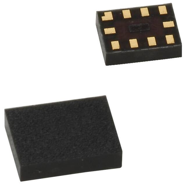
Package
10-Lead MicroPak™
1.6 x 2.1 mm, 0.5 mm Pitch
Ordering
Information
FSA832L10X
Applications
MP3, Mobile Internet Device (MID), Cell Phone, PDA,
Digital Camera, Notebook, and Netbook
Typical Application
Figure 1. Mobile Phone Example
© 2013 Fairchild Semiconductor Corporation
FSA832 • Rev. 1.0.1
www.fairchildsemi.com
FSA832 — USB2.0 High-Speed (480 Mbps) Charger Detector with Isolation Switch
August 2014
�Part
Number
Operating
Temperature Range
Top Mark
FSA832L10X
-40 to 85°C
ZY
Package Description
10-Lead, MicroPak™ 1.6 x 2.1 mm, 0.5 mm Pitch
Packing
Method
Tape & Reel
Pin Configurations
CHG_DET
10
9
VBUS
2
8
DM_CON
DP_HOST
3
7
DP_CON
CHG_AL_N
4
6
GND
SW_OPEN
1
DM_HOST
Control
5
GOOD_BAT
Figure 2.
Pin Assignments (Top View)
Pin Descriptions
Name
Pin #
Description
USB Interface
DP_HOST
3
D+ signal connected to the resident USB transceiver on the phone.
DM_HOST
2
D- signal connected to the resident USB transceiver on the phone.
VBUS
9
Input voltage supply pin to be connected to the VBUS pin of the USB connector.
Connector Interface
GND
6
Ground
DP_CON
7
Connected to the USB connector D+ pin
DM_CON
8
Connected to the USB connector D- pin
CHG_DET
10
CMOS push/pull output connected to charger IC to indicate if a charger has been detected
(LOW=charger not detected; HIGH=proprietary charger, DCP, or CDP charger detected).
SW_OPEN
1
Open-drain output pin; requires pull-up resistor to I/O voltage supply (LOW=switch closed;
Hi-Z=switch open).
CHG_AL_N
4
CMOS open-drain output pin (LOW=VBUS is valid and charge is allowed to be drawn from VBUS;
Hi-Z=VBUS is not at a valid voltage).
5
Input that indicates if the battery is a good battery or a dead battery (VIL=dead battery; VIH=good
battery).
Status Outputs
Input Pin
GOOD_BAT
Note:
1. Output voltage conditions are LOW = VOL and HIGH = VOH.
© 2013 Fairchild Semiconductor Corporation
FSA832 • Rev. 1.0.1
www.fairchildsemi.com
2
FSA832 — USB2.0 High-Speed (480 Mbps) Charger Detector with Isolation Switch
Ordering Information
�Functionality
Device Detected
GOOD_ SW_OP
EN
BAT
DCP
X
Proprietary Charger
Hi-Z
CHG_
AL_N
CHG_
DET
DP_HOST
DM_HOST
LOW
HIGH
Hi-Z
Hi-Z
DP_CON DM_CON
VDP_SRC(2)
Hi-Z(2)
Hi-Z
Hi-Z
X
Hi-Z
LOW
HIGH
Hi-Z
Hi-Z
HIGH
LOW
LOW
HIGH
DP_CON
DM_CON
LOW
Hi-Z
LOW
HIGH
Hi-Z
Hi-Z
VDP_SRC
Hi-Z
X
Hi-Z
LOW
LOW
Hi-Z
Hi-Z
Hi-Z
Hi-Z
SDP
HIGH
LOW
LOW
LOW
DP_CON
DM_CON
SDP
LOW
Hi-Z
LOW
LOW
Hi-Z
Hi-Z
VDP_SRC
Hi-Z
SDP, CDP, or DCP plugged
in and after 30-minute timer
expires
LOW
Hi-Z
Hi-Z
LOW
Hi-Z
Hi-Z
Hi-Z
Hi-Z
VBUS < VBUS valid to VBUS >
VBUS valid operation prior to
completing detection of
SDP, CDP, or DCP. Upon
detection, all outputs switch
as in rows above.
X
Hi-Z
Hi-Z
Hi-Z to
LOW
Hi-Z
Hi-Z
Hi-Z
Hi-Z
CDP
CDP
PS/2 Ports
(3)
DP_HOST DM_HOST
DP_HOST DM_HOST
Note:
2. Hi-Z is the internal state of DM_CON. Since a DCP has been detected, DM_CON is shorted to DP_CON externally and
DM_CON is shorted to VDP_SRC. VDP_SRC is not put on DP_CON for proprietary chargers.
3. DP_CON and DM_CON are pulled to VBUS through a resistor by the PS/2 port when it is connected to the FSA832.
Functional Description
absolute maximum VBUS voltage allowed. Whenever VBUS is
at GND, the FSA832 is completely off and the switches and
all I/Os are in the Hi-Z state. When VBUS climbs above the
valid VBUS threshold, detection occurs automatically and
CHG_DET, SW_OPEN, and CHG_AL_N all simultaneously
switch to the states indicated in Table 1 if GOOD_BAT is
HIGH (see Dead Battery Provision description for
GOOD_BAT = LOW).
Data Contact Detect (DCD)
DCD relies on the D+ and D- lines being present. DCD waits
until the internal timeout tDCD_TOUT has expired in the
following cases:
If a charger does not have a D+ pin on the USB connector;
If the D+ pin is not shorted to D- pin on the connector,
If D+ is pulled up to a supply; or
Dead Battery Provision
If D+ does not have a sufficient path to ground to defeat a
pull-up IDP_SRC (IDP_SRC) current source.
BC1.2 and USB 2.0 allow a portable device (defined as a
device with a battery) with a dead battery to take a maximum
of 100 mA from the USB VBUS line for a maximum of 45
minutes as long as the portable device forces the D+ line to
VDP_SRC. The FSA832 starts detection when VBUS crosses the
VBUSVLD threshold and, if it detects a CDP or SDP and
GOOD_BAT is HIGH, automatically closes the switch and
does not force the DP_CON pin to VDP_SRC.
The FSA832 proceeds with charger detection even though it
is unlikely that a charger is present. If there is no charge, the
algorithm reports an SDP and closes the switch. If a device
is pulling D+ HIGH, this voltage presents itself to the USB
transceiver or Physical Layer Interface (PHY) block within a
System on Chip (SoC) after the switch is closed.
Once charger detection is complete, the FSA832 starts a 30minute timer and forces the DP_CON pin to VDP_SRC until the
timer elapses. During the 30-minute period; if GOOD_BAT is
LOW, VDP_SRC is applied to DP_CON and the D+/D- switches
are opened. If GOOD_BAT is HIGH, VDP_SRC is not applied to
DP_CON and the D+/D- switches are closed. If GOOD_BAT
is LOW when the 30-minute timer expires; regardless of
whether a proprietary charger, SDP, CDP, or DCP was
previously detected; the FSA832 removes VDP_SRC from
DP_CON and forces CHG_DET LOW and CHG_AL_N to HiZ (SW_OPEN remains in Hi-Z). To exit this fault condition,
remove VBUS, wait for all the VBUS Printed Circuit Board
If the DCD timeout is insufficient and the PHY block is so
equipped, DCD and the charging algorithm can be repeated
in the PHY block. The stipulation is that the total time from
VBUS valid to USB transceiver connection with a 1.5 kΩ pullup to 3.3 V must be one (1) second, per USB 2.0 standards,
provided the portable device does not have a dead battery.
CHG_AL_N Output and Output Timing
CHG_AL_N output indicates that charge is allowed to be
drawn from VBUS when CHG_AL_N is LOW. When the
FSA832 first powers up and prior to detection, the
CHG_AL_N pin can follow VBUS up to 28 V, which is the
© 2013 Fairchild Semiconductor Corporation
FSA832 • Rev. 1.0.1
www.fairchildsemi.com
3
FSA832 — USB2.0 High-Speed (480 Mbps) Charger Detector with Isolation Switch
Table 1.
�PS/2 Port
Mice and keyboards utilizing the PS/2 port interface pull the
clock and data pins of the PS/2 connector HIGH to VBUS
through a resistive pull-up. When the PS/2 device is adapted
to a USB interface, the clock and data pins are translated to
the DP_CON and DM_CON lines of the USB connector,
respectively.
When GOOD_BAT is HIGH and the battery is removed from
the portable device while VBUS is valid, bringing GOOD_BAT
LOW; the FSA832 opens the isolation switches on DP_CON
and DM_CON and forces the DP_CON pin to VDP_SRC. In this
scenario, the timer generally expires because the SoC does
not have a supply to bring GOOD_BAT HIGH unless the
battery that was removed is re-inserted within 30 minutes
after the USB plug is inserted.
The benefit of detecting the PS/2 port as a separate device
is the ability to limit the current that can be drawn from the
bus, thus protecting the PS/2 port. Once the PS/2 port is
detected, the DP_HOST and DM_HOST switches remain
open to protect the USB PHY connected to DP_HOST and
DM_HOST from voltages as high as VBUS.
If an SDP or CDP is inserted with GOOD_BAT HIGH during
the 30-minute timer; then GOOD_BAT changes to LOW,
SW_OPEN changes to Hi-Z, and the counter continues
counting until the 30 minutes expires. If GOOD_BAT then
returns to HIGH, SW_OPEN changes to LOW and finishes
out the 30-minute time.
Ground Drops
When a DCP is detected, VDP_SRC is forced on DP_CON
provided GOOD_BAT is HIGH or GOOD_BAT is LOW and
the DBP timer has not expired. When ~1.5 A is flowing into
VBUS and GND lines of the USB cable, the current can create
substantial ground drops that lift the ground of the portable
device. This drop adds to the voltage at the DP_CON pin as
seen from the DCP D+ pin. For the maximum ground drop of
375 mV specified in the BC1.2 specification and for the
maximum VDP_SRC of 0.7 V; the voltage as seen by the DCP
would be 1.075 V. Smart DCPs that rely on this voltage
detection to determine attach and detach detection need to
take this into account.
GOOD_BAT has an internal pull-down resistor to ensure it is
LOW when the SoC is powered down. This input is designed
to have very VIH interface with low-voltage SoCs driven with
1.2 V supplies. GOOD_BAT can be connected to the
processor supply voltage becauses the processor should
wake up whenever VBUS is turned on.
Proprietary Chargers
Chargers pulling the USB data line DM_CON HIGH to 2.0 V
or 2.7 V and data line DP_CON HIGH to 2.0 V or 2.7 V are
detected by the FSA832 and reported proprietary chargers
with a higher charge current allowed. Other chargers that
float the DP/DM lines are also detected as a proprietary by
means of float detection. This allows a proprietary charger
with floating DP/DM to benefit from higher charge current.
VBUS Tolerance
When VBUS rises, an internal Power-On Reset (POR) detects
this voltage and prepares the FSA832 for charger detection.
VBUS voltages up to 28 V can be tolerated by the VBUS pin.
VBUS can tolerate voltages up to -2 V for cases where a
charger is plugged in backwards.
© 2013 Fairchild Semiconductor Corporation
FSA832 • Rev. 1.0.1
www.fairchildsemi.com
4
FSA832 — USB2.0 High-Speed (480 Mbps) Charger Detector with Isolation Switch
(PCB) capacitance to discharge, and re-apply VBUS. Table 1
provides the functionality of the pins when the timer expires.
�Stresses exceeding the absolute maximum ratings may damage the device. The device may not function or be operable
above the recommended operating conditions and stressing the parts to these levels is not recommended. In addition,
extended exposure to stresses above the recommended operating conditions may affect device reliability. The absolute
maximum ratings are stress ratings only.
Symbol
VBUS
Parameter
Voltage from USB Connector
Min.
Max.
Unit
-2
28
V
VSW
USB Switch I/O Voltage (DP_CON, DM_CON, DP_HOST, DM_HOST)
-0.5
6.0
V
ISW
USB Switch Current (DP_CON to DP_HOST, DM_CON to DM_HOST)
-30
+30
mA
VI/O
Voltage from GOOD_BAT, CHG_AL_N, CHG_DET and SW_OPEN I/Os
-0.5
6.0
V
VCA
Voltage from CHG_AL_N Output
-0.5
28.0
V
II/O
CHG_AL_N, CHG_DET and SW_OPEN Outputs Sink/Source Current
-5
+5
mA
Storage Temperature Range
-65
+150
°C
TSTG
TJ
Maximum Junction Temperature
+150
°C
TL
Lead Temperature (Soldering, 10 Seconds)
+260
°C
IEC 61000-4-2 System
ESD
USB Pins (DP_CON, DM_CON, VBUS)
Air Gap
15
Contact
8
Human Body Model, JEDEC JESD22-A114
All Pins
6
Charged Device Model, JEDEC JESD22-C101
All Pins
1
kV
Recommended Operating Conditions
The Recommended Operating Conditions table defines the conditions for actual device operation. Recommended operating
conditions are specified to ensure optimal performance to the datasheet specifications. Fairchild does not recommend
exceeding them or designing to Absolute Maximum Ratings.
Symbol
VBUS
VSW
TA
Parameter
VBUS Input HIGH Voltage
Switch I/O Voltage for USB Path
Operating Temperature
© 2013 Fairchild Semiconductor Corporation
FSA832 • Rev. 1.0.1
Min.
Max.
Unit
4
6
V
0
3.6
V
-40
+85
ºC
www.fairchildsemi.com
5
FSA832 — USB2.0 High-Speed (480 Mbps) Charger Detector with Isolation Switch
Absolute Maximum Ratings
�Unless otherwise indicated, VBUS=4 V to 6 V and TA=-40 to +85°C. Typical values are at TA=25°C unless otherwise specified.
Symbol
Parameter
Condition
Min.
Typ.
Max. Unit
Status Outputs
VOHCD
Output HIGH Voltage (CHG_DET)
IOH=-2 mA
2.0
V
VOL
Output LOW Voltage (CHG_DET,
CHG_AL_N, SW_OPEN)
IOL=2 mA
0.4
V
tDIFF
Skew Between Any Output (CHG_DET,
CHG_AL_N, SW_OPEN) Switching
Relative to Other Outputs Switching
II/O=±2 mA, CHG_AL_N=20 kΩ to
5 V, SW_OPEN=10 kΩ to 1.8 V
100
ns
4.0
V
3
µA
VBUS Pin
VBUSVLD VBUS Valid Detection Threshold(4)
IBUSIN
IVBUSACT
tOUT
0.8
VBUS Input Leakage
VBUS=0 V to 0.8 V
VBUS Active Mode Average Current
USB Path Active, USB Switch Closed
After Charger Detection
250
µA
Time from VBUS Valid Asserted to
CHG_DET, CHG_AL_N and SW_OPEN
Outputs Valid for BC1.2 Standard
Accessory Detection (SDP, DCP, or CDP)
DP_CON Pulled Down to GND with
15 kΩ; All Voltages Forced on VBUS,
DP_CON, DM_CON, and GND
simultaneously
250
ms
10
µA
6.0
Ω
Switch Characteristics
IOFF
RONUSB
Power Off Leakage Current
USB Path VBUS=0 V, VSW=0 V or
3.6 V, Figure 4
High-Speed USB Range Switch On
(4)
Resistance
VDP_CON / VDM_CON=0 V, 0.4 V;
ION=8 mA; Figure 3; VBUS=4 V to 6 V
4.5
Control Input
VIH
Input HIGH Voltage (GOOD_BAT)
1.1
V
VIL
Input LOW Voltage (GOOD_BAT)
RPD
Pull-Down Resistance (GOOD_BAT)
IIN
Input Leakage Current (GOOD_BAT)
VBUS=5 V, GOOD_BAT=0 V to 4.4 V
10
µA
IIOFF
Off-State Leakage Current (GOOD_BAT)
VBUS=0 V, GOOD_BAT=0 V to 4.4 V
10
µA
tDBP
Dead Battery Provision (DBP) Timer
45
min
tGB
Time from GOOD_BAT Asserted to SW_OPEN De-Asserted, Switches Closed
and Meet the RONUSB Specification
30
ms
tDB
Time from GOOD_BAT De-asserted to SW_OPEN Asserted, Switches Opened
65
ms
0.25
0.40
V
0.5
0.7
V
D+ Source Voltage
0.5
0.7
V
VLGC
Logic Threshold
0.8
2.0
V
IDM_SINK
D- Sink Current
25
175
µA
IDP_SINK
D+ Sink Current
25
175
µA
IDP_SRC
Data Contact Detect Current Source
7
13
µA
0.5
1
15
V
MΩ
30
Battery Charger Detection Parameters from BC1.2 Specification
VDAT_REF
Data Detect Voltage
VDM_SRC
(5)
VDP_SRC
D- Source Voltage
(5)
Continued on the following page…
© 2013 Fairchild Semiconductor Corporation
FSA832 • Rev. 1.0.1
www.fairchildsemi.com
6
FSA832 — USB2.0 High-Speed (480 Mbps) Charger Detector with Isolation Switch
DC Electrical Characteristics
�Unless otherwise indicated, VBUS=4 V to 6 V and TA=-40 to +85°C. Typical values are at TA=25°C unless otherwise specified.
Symbol
Parameter
Condition
Min.
Typ.
Max. Unit
tDCD_DBNC Data Contact Detect Debounce
10
ms
tDCD_TOUT Time for DCD to Timeout
300
tVDPSRC_ON D+ Voltage Source On Time
40
ms
tVDMSRC_ON D- Voltage Source On Time
40
ms
450
900
ms
Notes:
4. Guaranteed by characterization; not production tested.
5. The voltage source, VDP_SRC / VDM_SRC, is able to source at least 250 µA when the output voltage is in the specified range.
This voltage source should not pull DP_CON / DM_CON below 2.2 V when DP_CON / DM_CON is pulled to a voltage of
3.0 V minimum or 3.6 V maximum with a resistance of 900 Ω minimum or 1575 Ω maximum.
AC Electrical Characteristics
Unless otherwise specified, values are at TA=-40 to +85°C; all typical values are for VCC=3.3 V at TA=25°C.
Symbol
Parameter
Condition
Xtalk
Active Channel Crosstalk, DP_COM to
DM_CON(6)
Min.
Typ. Max.
F=1 MHz, RT=50 Ω, CL=0 pF
-78
F=240 MHz, RT=50 Ω,
CL=0 pF
-36
Off Isolation Rejection Ratio,
DM_HOST to DM_CON, DP_HOST to
(6)
DP_CON
f=1 MHz, RT=50 Ω, CL=0 pF
-84
OIRR
f=240 MHz, RT=50 Ω, CL=0 pF
-34
BW
Bandwidth of Switch(6)
RT=50 Ω
1.5
Unit
Figure
dB
Figure 6
dB
Figure 5
GHz
Figure 5
Note:
6. Guaranteed by characterization; not production tested.
Capacitance
Unless otherwise specified, values are at TA=-40 to +85°C.
Symbol
COFF
CON
Parameter
Condition
(7)
(7)
DP_CON, DM_CON Off Capacitance
DP_CON, DM_CON On Capacitance
Typical
Unit
Figure
VBIAS=0.2 V, f=1 MHz
3.2
pF
Figure 7
VBIAS=0.2 V, f=1 MHz
5.8
pF
Figure 8
Note:
7. Guaranteed by characterization; not production tested.
© 2013 Fairchild Semiconductor Corporation
FSA832 • Rev. 1.0.1
www.fairchildsemi.com
7
FSA832 — USB2.0 High-Speed (480 Mbps) Charger Detector with Isolation Switch
DC Electrical Characteristics
�VON
I A(OFF)
NC
nBn
A
nA
V IN
GND
Select
RON = VON / ION
V Sel =
V IN
I ON
Select
GND
VSel =
0 or Vcc
GND
0 orVcc
**Each switch port is tested separately.
Figure 3. On Resistance
Figure 4. Off Leakage
Network Analyzer
NC
Network Analyzer
RS
RS
VS1, S2, S3
VSel
GND
VOUT
RS and RT are functions of the application
environment (see AC tables for values).
CROSSTALK = 20 Log (VOUT / VIN
Figure 6. Active Channel Crosstalk
Figure 5. Channel Off Isolation
nBn
Capacitance
Meter
nSn
VSel =
RT
GND
GND
GND
Off-Isolation
= 20 Log (VOUT / VIN )
0 or Vcc
nBn
nSn
V Sel =
f = 1MHz
0 orV cc
nBn
nBn
Figure 7. Channel Off Capacitance
© 2013 Fairchild Semiconductor Corporation
FSA832 • Rev. 1.0.1
GND
RT
RS and RT are functions of the application
environment (see AC/DC tables).
f = 1MHz
RT
GND
VOUT
Capacitance
Meter
VS
GND
GND
GND
GND
VIN
VS
GND
RT
GND
Figure 8. Channel On Capacitance
www.fairchildsemi.com
8
FSA832 — USB2.0 High-Speed (480 Mbps) Charger Detector with Isolation Switch
Test Diagrams
�A
2.10±0.10
PIN#1 IDENT
IS 2X LONGER
THAN OTHER
LINES
B
1.60±0.10
1.62
KEEPOUT ZONE,
NO TRACES OR
VIAS ALLOWED
(0.11)
TOP VIEW
0.025±0.025
0.50±0.05
1.12
0.56
C
(0.35) 10X
SIDE VIEW
(0.25) 10X
0.50
C
(0.36) 2X
RECOMMENDED LAND PATTERN
0.60±0.05
(0.09) 10X
DETAIL A
1
4
0.20±0.05
(0.10±0.10)
0.20±0.05
0.56
5
10
0.30±0.05 9X
(0.31)
9
0.30±0.05
0.15±0.05
6
0.50
1.62
(0.20)
BOTTOM VIEW
0.20±0.05 9X
0.10
C A B
0.05
C
ALL FEATURES
NOTES:
A. PACKAGE CONFORMS TO JEDEC
REGISTRATION MO-255, VARIATION UABD.
B. DIMENSIONS ARE IN MILLIMETERS.
C. PRESENCE OF CENTER PAD IS PACKAGE
SUPPLIER DEPENDENT. IF PRESENT
IT IS NOT INTENDED TO BE SOLDERED
AND HAS A BLACK OXIDE FINISH.
D. DRAWING FILENAME: MKT-MAC10ArevG.
E. DIMENSIONS WITHIN ( ) ARE UNCONTROLLED.
0.30±0.05
DETAIL A
SCALE 2:1
�ON Semiconductor and
are trademarks of Semiconductor Components Industries, LLC dba ON Semiconductor or its subsidiaries in the United States and/or other countries.
ON Semiconductor owns the rights to a number of patents, trademarks, copyrights, trade secrets, and other intellectual property. A listing of ON Semiconductor’s product/patent
coverage may be accessed at www.onsemi.com/site/pdf/Patent−Marking.pdf. ON Semiconductor reserves the right to make changes without further notice to any products herein.
ON Semiconductor makes no warranty, representation or guarantee regarding the suitability of its products for any particular purpose, nor does ON Semiconductor assume any liability
arising out of the application or use of any product or circuit, and specifically disclaims any and all liability, including without limitation special, consequential or incidental damages.
Buyer is responsible for its products and applications using ON Semiconductor products, including compliance with all laws, regulations and safety requirements or standards,
regardless of any support or applications information provided by ON Semiconductor. “Typical” parameters which may be provided in ON Semiconductor data sheets and/or
specifications can and do vary in different applications and actual performance may vary over time. All operating parameters, including “Typicals” must be validated for each customer
application by customer’s technical experts. ON Semiconductor does not convey any license under its patent rights nor the rights of others. ON Semiconductor products are not
designed, intended, or authorized for use as a critical component in life support systems or any FDA Class 3 medical devices or medical devices with a same or similar classification
in a foreign jurisdiction or any devices intended for implantation in the human body. Should Buyer purchase or use ON Semiconductor products for any such unintended or unauthorized
application, Buyer shall indemnify and hold ON Semiconductor and its officers, employees, subsidiaries, affiliates, and distributors harmless against all claims, costs, damages, and
expenses, and reasonable attorney fees arising out of, directly or indirectly, any claim of personal injury or death associated with such unintended or unauthorized use, even if such
claim alleges that ON Semiconductor was negligent regarding the design or manufacture of the part. ON Semiconductor is an Equal Opportunity/Affirmative Action Employer. This
literature is subject to all applicable copyright laws and is not for resale in any manner.
PUBLICATION ORDERING INFORMATION
LITERATURE FULFILLMENT:
Literature Distribution Center for ON Semiconductor
19521 E. 32nd Pkwy, Aurora, Colorado 80011 USA
Phone: 303−675−2175 or 800−344−3860 Toll Free USA/Canada
Fax: 303−675−2176 or 800−344−3867 Toll Free USA/Canada
Email: orderlit@onsemi.com
© Semiconductor Components Industries, LLC
N. American Technical Support: 800−282−9855 Toll Free
USA/Canada
Europe, Middle East and Africa Technical Support:
Phone: 421 33 790 2910
Japan Customer Focus Center
Phone: 81−3−5817−1050
www.onsemi.com
1
ON Semiconductor Website: www.onsemi.com
Order Literature: http://www.onsemi.com/orderlit
For additional information, please contact your local
Sales Representative
www.onsemi.com
�


 工商网监
湘ICP备2023018690号
工商网监
湘ICP备2023018690号
