Is Now Part of
To learn more about ON Semiconductor, please visit our website at
www.onsemi.com
Please note: As part of the Fairchild Semiconductor integration, some of the Fairchild orderable part numbers
will need to change in order to meet ON Semiconductor’s system requirements. Since the ON Semiconductor
product management systems do not have the ability to manage part nomenclature that utilizes an underscore
(_), the underscore (_) in the Fairchild part numbers will be changed to a dash (-). This document may contain
device numbers with an underscore (_). Please check the ON Semiconductor website to verify the updated
device numbers. The most current and up-to-date ordering information can be found at www.onsemi.com. Please
email any questions regarding the system integration to Fairchild_questions@onsemi.com.
ON Semiconductor and the ON Semiconductor logo are trademarks of Semiconductor Components Industries, LLC dba ON Semiconductor or its subsidiaries in the United States and/or other countries. ON Semiconductor owns the rights to a number
of patents, trademarks, copyrights, trade secrets, and other intellectual property. A listing of ON Semiconductor’s product/patent coverage may be accessed at www.onsemi.com/site/pdf/Patent-Marking.pdf. ON Semiconductor reserves the right
to make changes without further notice to any products herein. ON Semiconductor makes no warranty, representation or guarantee regarding the suitability of its products for any particular purpose, nor does ON Semiconductor assume any liability
arising out of the application or use of any product or circuit, and specifically disclaims any and all liability, including without limitation special, consequential or incidental damages. Buyer is responsible for its products and applications using ON
Semiconductor products, including compliance with all laws, regulations and safety requirements or standards, regardless of any support or applications information provided by ON Semiconductor. “Typical” parameters which may be provided in ON
Semiconductor data sheets and/or specifications can and do vary in different applications and actual performance may vary over time. All operating parameters, including “Typicals” must be validated for each customer application by customer’s
technical experts. ON Semiconductor does not convey any license under its patent rights nor the rights of others. ON Semiconductor products are not designed, intended, or authorized for use as a critical component in life support systems or any FDA
Class 3 medical devices or medical devices with a same or similar classification in a foreign jurisdiction or any devices intended for implantation in the human body. Should Buyer purchase or use ON Semiconductor products for any such unintended
or unauthorized application, Buyer shall indemnify and hold ON Semiconductor and its officers, employees, subsidiaries, affiliates, and distributors harmless against all claims, costs, damages, and expenses, and reasonable attorney fees arising out
of, directly or indirectly, any claim of personal injury or death associated with such unintended or unauthorized use, even if such claim alleges that ON Semiconductor was negligent regarding the design or manufacture of the part. ON Semiconductor
is an Equal Opportunity/Affirmative Action Employer. This literature is subject to all applicable copyright laws and is not for resale in any manner.
�FSQ0765RS
Green-Mode Fairchild Power Switch (FPS™) for
Quasi-Resonant Operation - Low EMI and High Efficiency
Features
Description
! Optimized for Quasi-Resonant Converter (QRC)
A Quasi-Resonant Converter (QRC) generally shows
lower EMI and higher power conversion efficiency than a
conventional hard-switched converter with a fixed
switching frequency. The FSQ-series is an integrated
Pulse-Width Modulation (PWM) controller and
SenseFET specifically designed for quasi-resonant
operation and Alternating Valley Switching (AVS). The
PWM controller includes an integrated fixed-frequency
oscillator, Under-Voltage Lockout (UVLO), LeadingEdge Blanking (LEB), optimized gate driver, internal softstart, temperature-compensated precise current sources
for a loop compensation, and self-protection circuitry.
Compared with a discrete MOSFET and PWM controller
solution, the FSQ-series can reduce total cost,
component count, size, and weight; while simultaneously
increasing efficiency, productivity, and system reliability.
This device provides a basic platform for cost-effective
designs of quasi-resonant switching flyback converters.
! Low EMI through Variable Frequency Control and AVS
(Alternating Valley Switching)
! High Efficiency through Minimum Voltage Switching
! Narrow Frequency Variation Range over Wide Load
and Input Voltage Variation
! Advanced Burst-Mode Operation for Low Standby
Power Consumption
! Simple Scheme for Sync-Voltage Detection
! Pulse-by-Pulse Current Limit
! Various Protection functions: Overload Protection
!
!
!
!
(OLP), Over-Voltage Protection (OVP), Abnormal
Over-Current Protection (AOCP), Internal Thermal
Shutdown (TSD) with Hysteresis, Output Short
Protection (OSP)
Under-Voltage Lockout (UVLO) with Hysteresis
Internal Startup Circuit
Internal High-Voltage Sense FET (650V)
Built-in Soft-Start (17.5ms)
Applications
! Power Supply for LCD TV and Monitor, VCR, SVR,
STB, and DVD & DVD Recorder
! Adapter
Related Resources
Visit: http://www.fairchildsemi.com/apnotes/ for:
! AN-4134: Design Guidelines for Off-line Forward
!
!
!
!
!
!
!
Converters Using Fairchild Power Switch (FPS™)
AN-4137: Design Guidelines for Off-line Flyback
Converters Using Fairchild Power Switch (FPS™)
AN-4140: Transformer Design Consideration for
off-line Flyback Converters using Fairchild Power
Switch (FPS™)
AN-4141: Troubleshooting and Design Tips for
Fairchild Power Switch (FPS™) Flyback Applications
AN-4145: Electromagnetic Compatibility for Power
Converters
AN-4147: Design Guidelines for RCD Snubber of
Flyback Converters
AN-4148: Audible Noise Reduction Techniques for
FPS Applications
AN-4150: Design Guidelines for Flyback Converters
Using FSQ-series Fairchild Power Switch (FPS™)
© 2008 Fairchild Semiconductor Corporation
FSQ0765RS • Rev. 1.0.2
www.fairchildsemi.com
FSQ0765RS — Green-Mode Fairchild Power Switch (FPS™) for Quasi-Resonant Operation
March 2010
�Maximum Output Power(1)
Product
Number
PKG.(5)
Operating
Temp.
FSQ0765RSWDTU TO-220F-6L -25 to +85°C
230VAC±15%(2)
Current RDS(ON)
Limit
Max.
2.5A
Adapter(3)
1.6Ω
80W
85-265VAC
Open
Open
Adapter(3)
Frame(4)
Frame(4)
90W
48W
70W
Replaces
Devices
FSCM0765R
FSDM07652RE
Notes:
1. The junction temperature can limit the maximum output power.
2. 230VAC or 100/115VAC with doubler.
3. Typical continuous power in a non-ventilated enclosed adapter measured at 50°C ambient temperature.
4. Maximum practical continuous power in an open-frame design at 50°C ambient.
© 2008 Fairchild Semiconductor Corporation
FSQ0765RS • Rev. 1.0.2
www.fairchildsemi.com
2
FSQ0765RS — Green-Mode Fairchild Power Switch (FPS™) for Quasi-Resonant Operation
Ordering Information
�FSQ0765RS — Green-Mode Fairchild Power Switch (FPS™) for Quasi-Resonant Operation
Application Diagram
VO
AC
IN
Vstr
PWM
Sync
Drain
GND
VCC
FB
FSQ0765R Rev.00
Figure 1. Typical Flyback Application
Internal Block Diagram
Sync
5
AVS
Vstr
VCC
Drain
6
3
1
OSC
VCC
VCC
Vref
Idelay
FB
4
Vref
0.35/0.55
VBurst
VCC good
8V/12V
IFB
PWM
3R
R
SoftStart
S Q
LEB
250ns
Gate
driver
R Q
tON < tOSP
after SS
VOSP
LPF
AOCP
VSD
VCC
S
TSD
Q
2
VOCP
(1.1V)
GND
R Q
LPF
VOVP
VCC good
FSQ0765RS Rev.00
Figure 2. Internal Block Diagram
© 2008 Fairchild Semiconductor Corporation
FSQ0765RS • Rev. 1.0.2
www.fairchildsemi.com
3
�6. Vstr
5. Sync
4. FB
3. VCC
2. GND
1. Drain
FSQ0765R Rev.00
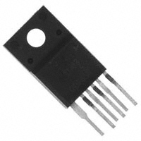
Figure 3. Pin Configuration (Top View)
Pin Definitions
Pin #
Name
1
Drain
SenseFET drain. High-voltage power SenseFET drain connection.
2
GND
Ground. This pin is the control ground and the SenseFET source.
3
VCC
Power Supply. This pin is the positive supply input, providing internal operating current for
both startup and steady-state operation.
4
FB
Feedback. This pin is internally connected to the inverting input of the PWM comparator. The
collector of an opto-coupler is typically tied to this pin. For stable operation, a capacitor should
be placed between this pin and GND. If the voltage of this pin reaches 6V, the overload protection triggers, which shuts down the FPS.
5
Sync
Sync. This pin is internally connected to the sync-detect comparator for quasi-resonant switching. In normal quasi-resonant operation, the threshold of the sync comparator is 1.2V/1.0V.
Vstr
Startup. This pin is connected directly, or through a resistor, to the high-voltage DC link. At
startup, the internal high-voltage current source supplies internal bias and charges the external capacitor connected to the VCC pin. Once VCC reaches 12V, the internal current source is
disabled. It is not recommended to connect Vstr and Drain together.
6
Description
© 2008 Fairchild Semiconductor Corporation
FSQ0765RS • Rev. 1.0.2
www.fairchildsemi.com
4
FSQ0765RS — Green-Mode Fairchild Power Switch (FPS™) for Quasi-Resonant Operation
Pin Configuration
�Stresses exceeding the absolute maximum ratings may damage the device. The device may not function or be operable above the recommended operating conditions and stressing the parts to these levels is not recommended. In addition, extended exposure to stresses above the recommended operating conditions may affect device reliability. The
absolute maximum ratings are stress ratings only. TA = 25°C, unless otherwise specified.
Symbol
Parameter
Min.
Max.
Unit
Vstr
Vstr Pin Voltage
500
V
VDS
Drain Pin Voltage
650
V
VCC
Supply Voltage
VFB
VSync
IDM
ID
20
Feedback Voltage Range
-0.3
Sync Pin Voltage
-0.3
VCC
Drain Current Pulsed
Continuous Drain Current(6)
(5)
V
V
13.0
V
14.4
A
TC = 25°C
3.60
TC = 100°C
2.28
A
EAS
Single Pulsed Avalanche Energy(7)
570
mJ
PD
Total Power Dissipation (TC=25°C)
45
W
TJ
Operating Junction Temperature
Internally limited
°C
TA
Operating Ambient Temperature
-25
+85
°C
-55
+150
°C
TSTG
ESD
Storage Temperature
Electrostatic Discharge
Protection
Human Body Model,
JESD22-A114
2.0
kV
Charged Device Model,
JESD22-C101
2.0
kV
Notes:
5. Guarenteed when external current applied to FB pin is lower than 100µA.
6. Repetitive rating: Pulse-width limited by maximum junction temperature.
7. L=81mH, starting TJ=25°C.
Thermal Impedance
TA = 25°C unless otherwise specified.
Symbol
Parameter
Package
Resistance(8)
θJA
Junction-to-Ambient Thermal
θJC
Junction-to-Case Thermal Resistance(9)
TO-220F-6L
Value
Unit
50
°C/W
2.8
°C/W
Notes:
8. Free standing with no heat-sink under natural convection.
9. Infinite cooling condition - refer to the SEMI G30-88.
© 2008 Fairchild Semiconductor Corporation
FSQ0765RS • Rev. 1.0.2
www.fairchildsemi.com
5
FSQ0765RS — Green-Mode Fairchild Power Switch (FPS™) for Quasi-Resonant Operation
Absolute Maximum Ratings
�TA = 25°C unless otherwise specified.
Symbol
Parameter
Conditions
Min.
650
Typ. Max. Units
SENSEFET SECTION
BVDSS
Drain Source Breakdown Voltage
VCC = 0V, ID = 100µA
IDSS
Zero-Gate-Voltage Drain Current
VDS = 520V, VGS = 0V
Drain-Source On-State Resistance
TJ = 25°C, ID = 1.8A
1.3
COSS
Output Capacitance
VGS = 0V, VDS = 25V, f = 1MHz
125
td(on)
Turn-On Delay Time
27
ns
Rise Time
102
ns
63
ns
65
ns
RDS(ON)
tr
td(off)
tf
VDD = 325V, ID = 6.5A
Turn-Off Delay Time
Fall Time
V
300
µA
1.6
Ω
pF
CONTROL SECTION
tON.MAX
Maximum On Time
TJ = 25°C
8.8
10.0
11.2
µs
tB
Blanking Time
TJ = 25°C, Vsync = 5V
13.2
15.0
16.8
µs
tW
Detection Time Window
TJ = 25°C, Vsync = 0V
fSW
Initial Switching Frequency
ΔfSW
tAVS
Switching Frequency Variation(11)
On Time
6.0
59.6
66.7
75.8
kHz
-25°C < TJ < 85°C
±5
±10
%
at VIN = 240VDC, Lm = 360μH
(AVS triggered when
VAVS>spec & tAVS


 工商网监
湘ICP备2023018690号
工商网监
湘ICP备2023018690号
