Is Now Part of
To learn more about ON Semiconductor, please visit our website at
www.onsemi.com
Please note: As part of the Fairchild Semiconductor integration, some of the Fairchild orderable part numbers
will need to change in order to meet ON Semiconductor’s system requirements. Since the ON Semiconductor
product management systems do not have the ability to manage part nomenclature that utilizes an underscore
(_), the underscore (_) in the Fairchild part numbers will be changed to a dash (-). This document may contain
device numbers with an underscore (_). Please check the ON Semiconductor website to verify the updated
device numbers. The most current and up-to-date ordering information can be found at www.onsemi.com. Please
email any questions regarding the system integration to Fairchild_questions@onsemi.com.
ON Semiconductor and the ON Semiconductor logo are trademarks of Semiconductor Components Industries, LLC dba ON Semiconductor or its subsidiaries in the United States and/or other countries. ON Semiconductor owns the rights to a number
of patents, trademarks, copyrights, trade secrets, and other intellectual property. A listing of ON Semiconductor’s product/patent coverage may be accessed at www.onsemi.com/site/pdf/Patent-Marking.pdf. ON Semiconductor reserves the right
to make changes without further notice to any products herein. ON Semiconductor makes no warranty, representation or guarantee regarding the suitability of its products for any particular purpose, nor does ON Semiconductor assume any liability
arising out of the application or use of any product or circuit, and specifically disclaims any and all liability, including without limitation special, consequential or incidental damages. Buyer is responsible for its products and applications using ON
Semiconductor products, including compliance with all laws, regulations and safety requirements or standards, regardless of any support or applications information provided by ON Semiconductor. “Typical” parameters which may be provided in ON
Semiconductor data sheets and/or specifications can and do vary in different applications and actual performance may vary over time. All operating parameters, including “Typicals” must be validated for each customer application by customer’s
technical experts. ON Semiconductor does not convey any license under its patent rights nor the rights of others. ON Semiconductor products are not designed, intended, or authorized for use as a critical component in life support systems or any FDA
Class 3 medical devices or medical devices with a same or similar classification in a foreign jurisdiction or any devices intended for implantation in the human body. Should Buyer purchase or use ON Semiconductor products for any such unintended
or unauthorized application, Buyer shall indemnify and hold ON Semiconductor and its officers, employees, subsidiaries, affiliates, and distributors harmless against all claims, costs, damages, and expenses, and reasonable attorney fees arising out
of, directly or indirectly, any claim of personal injury or death associated with such unintended or unauthorized use, even if such claim alleges that ON Semiconductor was negligent regarding the design or manufacture of the part. ON Semiconductor
is an Equal Opportunity/Affirmative Action Employer. This literature is subject to all applicable copyright laws and is not for resale in any manner.
�Revised June 2004
FXL5T244
Low Voltage Dual Supply 5-Bit Signal Translator
with Configurable Voltage Supplies
and Signal Levels and 3-STATE Outputs
General Description
Features
The FXL5T244 is a configurable dual-voltage-supply translator designed for one-way (unidirectional) voltage translation of signals between two voltage levels. The device
allows translation between voltages as high as 3.6V to as
low as 1.1V. A Inputs and the OE Control Pin track the VCCI
level, and Y Outputs track the VCCO level. Both inputs and
outputs are designed to accept supply voltage levels from
1.1V to 3.6V. This allows for unidirectional voltage translation over a variety of voltage levels: 1.2V, 1.5V, 1.8V, 2.5V,
and 3.3V.
■ One-way (unidirectional) translation between any
2 levels from 1.1V to 3.6V
The device remains in 3-STATE until both VCCs reach
active levels allowing either VCC to be powered-up first.
The device also contains power down control circuits that
place the device in 3-STATE if either VCC is removed. The
OE input, when HIGH, disables the outputs by placing
them in 3-STATE condition.
■ Fully configurable, inputs and outputs track respective
VCC levels
■ Non-preferential power-up sequencing; either VCC may
be powered-up first
■ Outputs remain in 3-STATE until active VCC level is
reached
■ Outputs switch to 3-STATE if either VCC is at GND
■ Power-off protection
■ Control input (OE) level is referenced to VCCI voltage
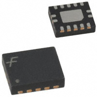
■ Packaged in 14-terminal DQFN (2.5mm x 3.0mm)
package
■ ESD protection exceeds:
• 4kV HBM ESD
(per JESD22-A114 & Mil Std 883e 3015.7)
• 8kV HBM I/O to GND ESD
(per JESD22-A114 & Mil Std 883e 3015.7)
• 1kV CDM ESD (per ESD STM 5.3)
• 200V MM ESD (per JESD22-A115 & ESD STM5.2)
Ordering Code:
Order Number
FXL5T244BQX
Package
Number
MLP014A
Package Description
14-Terminal Depopulated Quad Very-Thin Flat Pack No Leads (DQFN), JEDEC MO-241,
2.5 x 3.0mm
© 2004 Fairchild Semiconductor Corporation
DS500892
www.fairchildsemi.com
FXL5T244 Low Voltage Dual Supply 5-Bit Signal Translator with Configurable Voltage Supplies and Signal Levels
and 3-STATE Outputs
June 2004
�FXL5T244
Terminal Descriptions
Terminal
Names
Truth Table
Inputs
Description
OE
Output Enable Input
An
Data Inputs
Yn
3-STATE Outputs
VCCI
Inputs Power Supply
VCCO
Outputs Power Supply
GND
Ground
Outputs
OE
An
L
L
L
L
H
H
H
X
3-STATE
Yn
H = HIGH Voltage Level
L = LOW Voltage Level
X = Don’t Care
Connection Diagram
Terminal Assignment
Terminal Assignments for DQFN
Terminal Number
Terminal Name
1
VCCI
2
A0
3
A1
4
A2
5
A3
6
A4
7
GND
8
OE
9
Y4
10
Y3
11
Y2
12
Y1
13
Y0
14
VCCO
(Top View)
Power-Up/Power-Down Sequencing
FXL translators offer an advantage in that either VCC may
be powered up first. This benefit derives from the chip
design. When either VCC is at 0 volts, outputs are in a
HIGH-Impedance state. The control input, OE, is designed
to track the VCCI supply. A pull-up resistor tying OE to VCCI
should be used to ensure that bus contention, excessive
currents, or oscillations do not occur during power-up/
power-down. The size of the pull-up resistor is based upon
the current-sinking capability of the OE driver.
The recommended power-up sequence is the following:
1. Apply power to either VCC.
2. Apply power to the OE input (Logic HIGH for A-to-B
operation; Logic LOW for B-to-A operation) and to the
respective data inputs (A Port or B Port). This may
occur at the same time as Step 1.
3. Apply power to other VCC.
4. Drive the OE input LOW to enable the device.
The recommended power-down sequence is the following:
1. Drive OE input HIGH to disable the device.
2. Remove power from either VCC.
3. Remove power from other VCC.
www.fairchildsemi.com
2
�Recommended Operating
Conditions (Note 3)
Supply Voltage
VCCI
−0.5V to +4.6V
Power Supply Operating (VCCI or VCCO)
VCCO
−0.5V to +4.6V
Input Voltage
−0.5V to +4.6V
DC Input Voltage (VI)
Output Voltage (VO) (Note 2)
−0.5V to +4.6V
Outputs 3-STATE
Outputs Active
An
0.0V to 3.6V
Control Inputs (OE)
0.0V to 3.6V
Output Current in IOH/IOL
−0.5V to VCCO + 0.5V
VCCO = 3.0V to 3.6V
±24 mA
−50 mA
VCCO = 2.3V to 2.7V
±18 mA
DC Input Diode Current (IIK) VI < 0V
VCCO = 1.65V to 1.95V
DC Output Diode Current (IOK)
VO < 0V
−50 mA
VCCO = 1.4V to 1.65V
VO > VCC
+50 mA
VCCO = 1.1V to 1.4V
DC Output Source/Sink Current
±2 mA
±0.5 mA
−40°C to +85°C
Minimum Input Edge Rate (∆V/∆t)
VCCA/B = 1.1V to 3.6V
DC VCC or Ground Current per
10 ns/V
±100 mA
Supply Pin (ICC or GND)
Storage Temperature Range (TSTG)
±6 mA
Free Air Operating Temperature (TA)
−50 mA / +50 mA
(IOH/IOL)
1.1V to 3.6V
−65°C to +150°C
Note 1: The “Absolute Maximum Ratings” are those values beyond which
the safety of the device cannot be guaranteed. The device should not be
operated at these limits. The parametric values defined in the Electrical
Characteristics tables are not guaranteed at the absolute maximum ratings.
The “Recommended Operating Conditions” table will define the conditions
for actual device operation.
Note 2: IO Absolute Maximum Rating must be observed.
Note 3: All unused inputs must be held at VCCI or GND.
DC Electrical Characteristics
Symbol
VIH
Parameter
Conditions
High Level Input Voltage
VCCI
VCCO
(V)
(V)
2.7 - 3.6
VIL
Low Level Input Voltage
Max
1.6
1.1 - 3.6
0.65 x VCCI
1.4 - 1.65
0.65 x VCCI
1.1 - 1.4
0.9 x VCCI
V
2.7 - 3.6
0.8
2.3 - 2.7
0.7
1.65 - 2.3
1.1 - 3.6
0.35 x VCCI
1.4 - 1.65
High Level Output Voltage
0.1 x VCCI
IOH = −100 µA
1.1 - 3.6
1.1 - 3.6
VCC0 - 0.2
IOH = −12 mA
2.7
2.7
2.2
IOH = −18 mA
3.0
3.0
2.4
IOH = −24 mA
3.0
3.0
2.2
IOH = −6 mA
2.3
2.3
2.0
IOH = −12 mA
2.3
2.3
1.8
V
IOH = −18 mA
2.3
2.3
1.7
IOH = −6 mA
1.65
1.65
1.25
IOH = −2 mA
1.4
1.4
1.05
IOH = −0.5 mA
1.1
1.1
0.75 x VCC0
3
V
0.35 x VCCI
1.1 - 1.4
VOH
Units
2.0
2.3 - 2.7
1.65 - 2.3
Min
www.fairchildsemi.com
FXL5T244
Absolute Maximum Ratings(Note 1)
�FXL5T244
DC Electrical Characteristics
Symbol
VOL
Parameter
Low Level Output Voltage
(Continued)
VCCI
VCCO
(V)
(V)
IOL = 100µA
1.1 - 3.6
1.1- 3.6
0.2
IOL = 12 mA
2.7
2.7
0.4
IOL = 18 mA
3.0
3.0
0.4
IOL = 24 mA
3.0
3.0
0.55
IOL = 12 mA
2.3
2.3
0.4
IOL = 18 mA
2.3
2.3
0.6
IOL = 6 mA
1.65
1.65
0.3
IOL = 2 mA
1.4
1.4
0.35
0.3 x VCCI
Conditions
IOL = 0.5 mA
Min
Max
1.1
1.1
1.1 - 3.6
3.6
±1.0
0
3.6
±10.0
Yn = 0V to 3.6V
3.6
0
±10.0
II
Input Leakage Current
VI = V CCI or GND
IOFF
Power Off Leakage Current
An, OE = 0V to 3.6V
IOZ
3-STATE Output Leakage
OE = VIH
3.6
3.6
±10.0
(Note 4)
0 ≤ V O ≤ 3.6V
OE = Don’t Care
0
3.6
+10.0
VI = VIH or VIL
OE = Don’t Care
3.6
0
+10.0
Units
V
µA
µA
µA
ICCI/O (Note 4) Quiescent Supply Current
VI = V CCI or GND; IO = 0
1.1 - 3.6
1.1 - 3.6
20.0
µA
ICCZ (Note 5)
Quiescent Supply Current
VI = V CCI or GND; IO = 0
1.1 - 3.6
1.1 - 3.6
20.0
µA
ICCI
Quiescent Supply Current
VI = V CCI or GND; IO = 0
0
1.1 - 3.6
−10.0
µA
VI = V CCI or GND; IO = 0
1.1 - 3.6
0
10.0
µA
VI = V CCO or GND; IO = 0
1.1 - 3.6
0
−10.0
µA
VI = V CCO or GND; IO = 0
0
1.1 - 3.6
10.0
µA
3.6
3.6
500
µA
ICCO
∆ICCI/O
Quiescent Supply Current
Increase in ICC per Input;
VIH = 3.0
Other Inputs at VCC or GND
Note 4: Don’t Care = Any valid logic level.
Note 5: Reflects current per supply, VCCI or VCCO.
www.fairchildsemi.com
4
�TA = −40°C to +85°C
Symbol
VCCO =
3.0V to 3.6V
Parameter
VCCO =
2.3V to 2.7V
VCCO =
1.65V to 1.95V
VCCO =
1.4V to 1.6V
VCCO =
1.1V to 1.3V
Units
Min
Max
Min
Max
Min
Max
Min
Max
Min
Max
tPLH, tPHL Propagation Delay A to Y
0.2
3.5
0.3
3.9
0.7
5.4
0.8
6.8
1.4
22.0
ns
tPZH, tPZL Output Enable OE to Y
0.5
4.0
0.7
4.4
1.0
5.9
1.0
6.4
1.5
17.0
ns
tPHZ, tPLZ Output Disable OE to Y
0.2
3.8
0.2
4.0
0.7
4.8
1.5
6.2
2.0
17.0
ns
AC Electrical Characteristics VCCI = 2.3V to 2.7V
TA = −40°C to +85°C
Symbol
VCCO =
3.0V to 3.6V
Parameter
VCCO =
2.3V to 2.7V
VCCO =
1.65V to 1.95V
VCCO =
1.4V to 1.6V
VCCO =
1.1V to 1.3V
Units
Min
Max
Min
Max
Min
Max
Min
Max
Min
Max
tPLH, tPHL Propagation Delay A toY
0.2
3.8
0.4
4.2
0.5
5.6
0.8
6.9
1.4
22.0
ns
tPZH, tPZL Output Enable OE to Y
0.6
4.2
0.8
4.6
1.0
6.0
1.0
6.8
1.5
17.0
ns
tPHZ, tPLZ Output Disable OE to Y
0.2
4.1
0.2
4.3
0.7
4.8
1.5
6.7
2.0
17.0
ns
AC Electrical Characteristics VCCI = 1.65V to 1.95V
TA = −40°C to +85°C
Symbol
VCCO =
3.0V to 3.6V
Parameter
VCCO =
2.3V to 2.7V
VCCO =
1.65V to 1.95V
VCCO =
1.4V to 1.6V
VCCO =
1.1V to 1.3V
Units
Min
Max
Min
Max
Min
Max
Min
Max
Min
Max
tPLH, tPHL Propagation Delay A to Y
0.3
4.0
0.5
4.5
0.8
5.7
0.9
7.1
1.5
22.0
ns
tPZH, tPZL Output Enable OE to Y
0.6
5.2
0.8
5.4
1.2
6.9
1.2
7.2
1.5
18.0
ns
tPHZ, tPLZ Output Disable OE to Y
0.2
5.1
0.2
4.0
0.8
5.2
1.5
7.0
2.0
17.0
ns
AC Electrical Characteristics VCCI = 1.4V to 1.6V
TA = −40°C to +85°C
Symbol
VCCO =
3.0V to 3.6V
Parameter
VCCO =
2.3V to 2.7V
VCCO =
1.65V to 1.95V
VCCO =
1.4V to 1.6V
VCCO =
1.1V to 1.3V
Units
Min
Max
Min
Max
Min
Max
Min
Max
Min
Max
tPLH, tPHL Propagation Delay A to Y
0.5
4.3
0.5
4.8
1.0
6.0
1.0
7.3
1.5
22.0
ns
tPZH, tPZL Output Enable OE to Y
1.1
7.5
1.1
7.6
1.3
7.7
1.4
7.9
2.0
20.0
ns
tPHZ, tPLZ Output Disable OE to Y
0.4
6.1
0.4
6.2
0.9
6.2
1.5
7.5
2.0
18.0
ns
AC Electrical Characteristics VCCI = 1.1V to 1.3V
TA = −40°C to +85°C
Symbol
VCCO =
3.0V to 3.6V
Parameter
VCCO =
2.3V to 2.7V
VCCO =
1.65V to 1.95V
VCCO =
1.4V to 1.6V
VCCO =
1.1V to 1.3V
Units
Min
Max
Min
Max
Min
Max
Min
Max
Min
Max
tPLH, tPHL Propagation Delay A to Y
0.8
13.0
1.0
7.0
1.2
8.0
1.3
9.5
2.0
24.0
ns
tPZH, tPZL Output Enable OE to Y
1.0
12.0
1.0
9.0
2.0
10.0
2.0
11.0
2.0
24.0
ns
tPHZ, tPLZ Output Disable OE to Y
1.0
15.0
0.7
7.0
1.0
8.0
2.0
10.0
2.0
20.0
ns
Capacitance
Symbol
Parameter
Conditions
TA = +25°C
Typical
Units
CIN
Input Capacitance An Control Pin (OE)
VCCI = VCCO = 3.3V, VI = 0V or VCCI
4.0
COUT
Output Capacitance Yn
VCCI = VCCO = 3.3V, VI = 0V or VCCI
5.0
pF
CPD
Power Dissipation Capacitance
VCCI = VCCO = 3.3V, VI = 0V or VCCI, F = 10 MHz
20.0
pF
5
pF
www.fairchildsemi.com
FXL5T244
AC Electrical Characteristics VCCI = 3.0V to 3.6V
�FXL5T244
AC Loading and Waveforms
TEST
SWITCH
tPLH, tPHL
OPEN
tPLZ, tPZL
VCCO x 2 at VCCO = 3.3 ± 0.3V, 2.5V ± 0.2V,
1.8V ± 0.15V, 1.5V ± 0.1V, 1.2V ± 0.1V
tPHZ, tPZH
GND
FIGURE 1. AC Test Circuit
AC Load Table
VCCO
CL
RL
Rtr1
1.2V ± 0.1V
15 pF
2 kΩ
2 kΩ
1.5V ± 0.1V
15 pF
2 kΩ
2 kΩ
1.8V ± 0.15V
15 pF
2 kΩ
2 kΩ
2.5V ± 0.2V
15 pF
2 kΩ
2 kΩ
3.3V ± 0.3V
15 pF
2 kΩ
2 kΩ
Note: Input tR = tF = 2.0 ns, 10% to 90%
Note: Input t R = tF = 2.0 ns, 10% to 90%
Input tR = tF = 2.5ns, 10% to 90%, @ VI = 3.0V to 3.6V only
Input tR = tF = 2.5ns, 10% to 90%, @ VI = 3.0V to 3.6V only
FIGURE 2. Waveform for Inverting
and Non-Inverting Functions
FIGURE 3. 3-STATE Output Low Enable
and Disable Times for Low Voltage Logic
Note: Input tR = tF = 2.0 ns, 10% to 90%
Input tR = tF = 2.5ns, 10% to 90%, @ VI = 3.0V to 3.6V only
FIGURE 4. 3-STATE Output High Enable and Disable Times for Low Voltage Logic
Symbol
VCC
3.3V ± 0.3V
2.5V ± 0.2V
1.8V ± 0.15V
1.5V ± 0.1V
Vmi
VCCI/2
VCCI/2
VCCI/2
VCCI/2
VCCI/2
Vmo
VCCO/2
VCCO/2
VCCO/2
VCCO/2
VCCO/2
VX
VOH − 0.3V
VOH − 0.15V
VOH − 0.15V
VOH − 0.1V
VOH − 0.1V
VY
VOL + 0.3V
VOL + 0.15V
VOL + 0.15V
VOL + 01V
VOL + 01V
Note: For Vmi: VCCI = VCCA for Control Pins T/R and OE, or VCCA/2
www.fairchildsemi.com
6
1.2V ± 0.1V
�Tape Format for DQFN
Package
Designator
BQX
Tape
Number
Cavity
Section
Cavities
Status
Cover Tape
Status
Leader (Start End)
125 (typ)
Empty
Sealed
Carrier
3000
Filled
Sealed
Trailer (Hub End)
75 (typ)
Empty
Sealed
TAPE DIMENSIONS inches (millimeters)
REEL DIMENSIONS inches (millimeters)
Tape Size
12 mm
A
B
C
D
N
W1
W2
13.0
0.059
0.512
0.795
2.165
0.488
0.724
(330.0)
(1.50)
(13.00)
(20.20)
(55.00)
(12.4)
(18.4)
7
www.fairchildsemi.com
FXL5T244
Tape and Reel Specification
�FXL5T244 Low Voltage Dual Supply 5-Bit Signal Translator with Configurable Voltage Supplies and Signal Levels
and 3-STATE Outputs
Physical Dimensions inches (millimeters) unless otherwise noted
14-Terminal Depopulated Quad Very-Thin Flat Pack No Leads (DQFN), JEDEC MO-241, 2.5 x 3.0mm
Package Number MLP014A
Fairchild does not assume any responsibility for use of any circuitry described, no circuit patent licenses are implied and
Fairchild reserves the right at any time without notice to change said circuitry and specifications.
LIFE SUPPORT POLICY
FAIRCHILD’S PRODUCTS ARE NOT AUTHORIZED FOR USE AS CRITICAL COMPONENTS IN LIFE SUPPORT
DEVICES OR SYSTEMS WITHOUT THE EXPRESS WRITTEN APPROVAL OF THE PRESIDENT OF FAIRCHILD
SEMICONDUCTOR CORPORATION. As used herein:
2. A critical component in any component of a life support
device or system whose failure to perform can be reasonably expected to cause the failure of the life support
device or system, or to affect its safety or effectiveness.
1. Life support devices or systems are devices or systems
which, (a) are intended for surgical implant into the
body, or (b) support or sustain life, and (c) whose failure
to perform when properly used in accordance with
instructions for use provided in the labeling, can be reasonably expected to result in a significant injury to the
user.
www.fairchildsemi.com
www.fairchildsemi.com
8
�ON Semiconductor and
are trademarks of Semiconductor Components Industries, LLC dba ON Semiconductor or its subsidiaries in the United States and/or other countries.
ON Semiconductor owns the rights to a number of patents, trademarks, copyrights, trade secrets, and other intellectual property. A listing of ON Semiconductor’s product/patent
coverage may be accessed at www.onsemi.com/site/pdf/Patent−Marking.pdf. ON Semiconductor reserves the right to make changes without further notice to any products herein.
ON Semiconductor makes no warranty, representation or guarantee regarding the suitability of its products for any particular purpose, nor does ON Semiconductor assume any liability
arising out of the application or use of any product or circuit, and specifically disclaims any and all liability, including without limitation special, consequential or incidental damages.
Buyer is responsible for its products and applications using ON Semiconductor products, including compliance with all laws, regulations and safety requirements or standards,
regardless of any support or applications information provided by ON Semiconductor. “Typical” parameters which may be provided in ON Semiconductor data sheets and/or
specifications can and do vary in different applications and actual performance may vary over time. All operating parameters, including “Typicals” must be validated for each customer
application by customer’s technical experts. ON Semiconductor does not convey any license under its patent rights nor the rights of others. ON Semiconductor products are not
designed, intended, or authorized for use as a critical component in life support systems or any FDA Class 3 medical devices or medical devices with a same or similar classification
in a foreign jurisdiction or any devices intended for implantation in the human body. Should Buyer purchase or use ON Semiconductor products for any such unintended or unauthorized
application, Buyer shall indemnify and hold ON Semiconductor and its officers, employees, subsidiaries, affiliates, and distributors harmless against all claims, costs, damages, and
expenses, and reasonable attorney fees arising out of, directly or indirectly, any claim of personal injury or death associated with such unintended or unauthorized use, even if such
claim alleges that ON Semiconductor was negligent regarding the design or manufacture of the part. ON Semiconductor is an Equal Opportunity/Affirmative Action Employer. This
literature is subject to all applicable copyright laws and is not for resale in any manner.
PUBLICATION ORDERING INFORMATION
LITERATURE FULFILLMENT:
Literature Distribution Center for ON Semiconductor
19521 E. 32nd Pkwy, Aurora, Colorado 80011 USA
Phone: 303−675−2175 or 800−344−3860 Toll Free USA/Canada
Fax: 303−675−2176 or 800−344−3867 Toll Free USA/Canada
Email: orderlit@onsemi.com
© Semiconductor Components Industries, LLC
N. American Technical Support: 800−282−9855 Toll Free
USA/Canada
Europe, Middle East and Africa Technical Support:
Phone: 421 33 790 2910
Japan Customer Focus Center
Phone: 81−3−5817−1050
www.onsemi.com
1
ON Semiconductor Website: www.onsemi.com
Order Literature: http://www.onsemi.com/orderlit
For additional information, please contact your local
Sales Representative
www.onsemi.com
�


 工商网监
湘ICP备2023018690号
工商网监
湘ICP备2023018690号
