DATA SHEET
www.onsemi.com
PNP Epitaxial Silicon
Transistor
KSA1015
1
Features
•
•
•
•
Low−Frequency Amplifier
Collector−Base Voltage: VCBO = −50 V
Complement to KSC1815
These Devices are Pb−Free, Halogen Free/BFR Free and are RoHS
Compliant
Parameter
Value
Unit
VCBO
Collector−Base Voltage
−50
V
VCEO
Collector−Emitter Voltage
−50
V
VEBO
Emitter−Base Voltage
−5
V
IC
Collector Current
−150
mA
IB
Base Current
−50
mA
TJ
Junction Temperature
150
°C
−55 to 150
°C
TSTG
Storage Temperature Range
3
Bent Lead
Tape & Reel
Ammo Packing
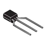
TO−92 3 4.83x4.76 LEADFORMED
CASE 135AR
ABSOLUTE MAXIMUM RATINGS (TA = 25°C unless otherwise noted)
Symbol
2
1. Emitter
2. Collector
3. Base
MARKING DIAGRAM
A1015
(GR, Y)
AYWW
A
A1015(GR, Y)
Y
WW
= Assembly Site
= Device Code
= Year of Production,
= Work Week Number
Stresses exceeding those listed in the Maximum Ratings table may damage the
device. If any of these limits are exceeded, device functionality should not be
assumed, damage may occur and reliability may be affected.
ORDERING INFORMATION
THERMAL CHARACTERISTICS (Note 1)
(TA = 25°C unless otherwise noted)
Parameter
Max
Unit
Total Device Dissipation
400
mW
Derate Above 25°C
3.2
mW/°C
Thermal Resistance, Junction to Ambient
312
°C/W
Symbol
PD
RqJA
Packing
Method
Device
Marking
Package
KSA1015GRTA
A1015GR
TO−92 3L
(Pb−Free)
Ammo
A1015Y
TO−92 3L
(Pb−Free)
Ammo
KSA1015YTA
1. PCB size: FR−4, 76 mm x 114 mm x 1.57 mm (3.0 inch x 4.5 inch x 0.062 inch)
with minimum land pattern size.
© Semiconductor Components Industries, LLC, 2002
December, 2021 − Rev. 2
1
Publication Order Number:
KSA1015/D
�KSA1015
ELECTRICAL CHARACTERISTICS (TA = 25°C unless otherwise noted)
Symbol
Min
Typ
Max
Unit
BVCBO
Collector−Base Breakdown Voltage
Parameter
IC = −100 mA, IE = 0
Conditions
−50
−
−
V
BVCEO
Collector−Emitter Breakdown Voltage
IC = −10 mA, IB = 0
−50
−
−
V
BVEBO
Emitter−Base Breakdown Voltage
IE = −10 mA, IC = 0
−5
−
−
V
ICBO
Collector Cut−Off Current
VCB = −50 V, IE = 0
−
−
−0.1
mA
IEBO
Emitter Cut−Off Current
VEB = −5 V, IC = 0
−
−
−0.1
mA
hFE1
DC Current Gain
VCE = −6 V, IC = −2 mA
70
−
400
hFE2
DC Current Gain
VCE = −6 V, IC = −150 mA
25
−
−
VCE(sat)
Collector−Emitter Saturation Voltage
IC = −100 mA, IB = −10 mA
−
−0.1
−0.3
VBE(sat)
Base−Emitter Saturation Voltage
IC = −100 mA, IB = −10 mA
−
−
−1.1
V
fT
Current Gain Bandwidth Product
VCE = −10 V, IC = −1 mA
80
−
−
MHz
Cob
Output Capacitance
VCB = −10 V, IE = 0, f = 1 MHz
−
4
7
pF
NF
Noise Figure
VCE = −6 V, IC = −0.1 mA, f = 100 Hz,
RG = 10 kW
−
0.5
6
dB
V
Product parametric performance is indicated in the Electrical Characteristics for the listed test conditions, unless otherwise noted. Product
performance may not be indicated by the Electrical Characteristics if operated under different conditions.
hFE CLASSIFICATION
Classification
O
Y
GR
hFE1
70~140
120~240
200~400
www.onsemi.com
2
�KSA1015
TYPICAL PERFORMANCE CHARACTERISTICS
1000
−45
VCE = −6 V
IB = −400 mA
IB = −350 mA
IB = −300 mA
IB = −250 mA
−40
−35
−30
hFE, DC CURRENT GAIN
IC, COLLECTOR CURRENT (V)
−50
IB = −200 mA
−25
IB = −150 mA
−20
−15
IB = −100 mA
−10
IB = −50 mA
100
10
−5
0
0
1
−0.1
−2 −4 −6 −8 −10 −12 −14 −16 −18 −20
VCE, COLLECTOR−EMITTER VOLTAGE (V)
−1
VBE(sat)
−0.1
VCE(sat)
−0.01
−0.1
VCE = −6 V
IC, COLLECTOR CURRENT (mA)
VBE(sat), VCE(sat), SATURATION VOLTAGE (V)
−100
IC = 10 IB
−1
−10
−10
−1
−0.1
−0.0
−100
IC, COLLECTOR CURRENT (mA)
−0.2
−0.4
−0.6
−0.8
−1.0
VBE(sat), BASE−EMITTER VOLTAGE (V)
Figure 3. Base−Emitter Saturation Voltage
and Collector−Emitter Saturation Voltage
Figure 4. Base−Emitter On Voltage
1000
f = 1 MHz
IE = 0
VCE = −6 V
hFE, DC CURRENT GAIN
Cob, CAPACITANCE (pF)
−100
Figure 2. DC Current Gain
−10
1
−1
−10
IC, COLLECTOR CURRENT (mA)
Figure 1. Static Characteristic
10
−1
−10
100
10
−100
VCB(sat), COLLECTOR−BASE VOLTAGE (V)
−1
−10
IC, COLLECTOR CURRENT (mA)
Figure 5. Collector Output Capacitance
Figure 6. Current Gain Bandwidth Product
www.onsemi.com
3
−1.2
�MECHANICAL CASE OUTLINE
PACKAGE DIMENSIONS
TO−92 3 4.83x4.76 LEADFORMED
CASE 135AR
ISSUE O
DOCUMENT NUMBER:
DESCRIPTION:
98AON13879G
DATE 30 SEP 2016
Electronic versions are uncontrolled except when accessed directly from the Document Repository.
Printed versions are uncontrolled except when stamped “CONTROLLED COPY” in red.
TO−92 3 4.83X4.76 LEADFORMED
PAGE 1 OF 1
ON Semiconductor and
are trademarks of Semiconductor Components Industries, LLC dba ON Semiconductor or its subsidiaries in the United States and/or other countries.
ON Semiconductor reserves the right to make changes without further notice to any products herein. ON Semiconductor makes no warranty, representation or guarantee regarding
the suitability of its products for any particular purpose, nor does ON Semiconductor assume any liability arising out of the application or use of any product or circuit, and specifically
disclaims any and all liability, including without limitation special, consequential or incidental damages. ON Semiconductor does not convey any license under its patent rights nor the
rights of others.
© Semiconductor Components Industries, LLC, 2019
www.onsemi.com
�onsemi,
, and other names, marks, and brands are registered and/or common law trademarks of Semiconductor Components Industries, LLC dba “onsemi” or its affiliates
and/or subsidiaries in the United States and/or other countries. onsemi owns the rights to a number of patents, trademarks, copyrights, trade secrets, and other intellectual property.
A listing of onsemi’s product/patent coverage may be accessed at www.onsemi.com/site/pdf/Patent−Marking.pdf. onsemi reserves the right to make changes at any time to any
products or information herein, without notice. The information herein is provided “as−is” and onsemi makes no warranty, representation or guarantee regarding the accuracy of the
information, product features, availability, functionality, or suitability of its products for any particular purpose, nor does onsemi assume any liability arising out of the application or use
of any product or circuit, and specifically disclaims any and all liability, including without limitation special, consequential or incidental damages. Buyer is responsible for its products
and applications using onsemi products, including compliance with all laws, regulations and safety requirements or standards, regardless of any support or applications information
provided by onsemi. “Typical” parameters which may be provided in onsemi data sheets and/or specifications can and do vary in different applications and actual performance may
vary over time. All operating parameters, including “Typicals” must be validated for each customer application by customer’s technical experts. onsemi does not convey any license
under any of its intellectual property rights nor the rights of others. onsemi products are not designed, intended, or authorized for use as a critical component in life support systems
or any FDA Class 3 medical devices or medical devices with a same or similar classification in a foreign jurisdiction or any devices intended for implantation in the human body. Should
Buyer purchase or use onsemi products for any such unintended or unauthorized application, Buyer shall indemnify and hold onsemi and its officers, employees, subsidiaries, affiliates,
and distributors harmless against all claims, costs, damages, and expenses, and reasonable attorney fees arising out of, directly or indirectly, any claim of personal injury or death
associated with such unintended or unauthorized use, even if such claim alleges that onsemi was negligent regarding the design or manufacture of the part. onsemi is an Equal
Opportunity/Affirmative Action Employer. This literature is subject to all applicable copyright laws and is not for resale in any manner.
PUBLICATION ORDERING INFORMATION
LITERATURE FULFILLMENT:
Email Requests to: orderlit@onsemi.com
onsemi Website: www.onsemi.com
◊
TECHNICAL SUPPORT
North American Technical Support:
Voice Mail: 1 800−282−9855 Toll Free USA/Canada
Phone: 011 421 33 790 2910
Europe, Middle East and Africa Technical Support:
Phone: 00421 33 790 2910
For additional information, please contact your local Sales Representative
�


 工商网监
湘ICP备2023018690号
工商网监
湘ICP备2023018690号
