Single Channel Operational
Amplifier
LM321
LM321 is a general purpose, single channel op amp with internal
compensation and a true differential input stage. This op amp features
a wide supply voltage ranging from 3 V to 32 V for single supplies and
±1.5 to ±16 V for split supplies, suiting a variety of applications.
LM321 is unity gain stable even with large capacitive loads up to
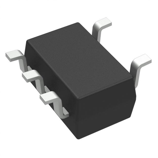
1.5 nF. LM321 is available in a space-saving TSOP−5/SOT23−5
package.
www.onsemi.com
5
1
Features
•
•
•
•
•
•
•
•
Wide Supply Voltage Range: 3 V to 32 V
Short Circuit Protected Outputs
True Differential Input Stage
Low Input Bias Currents
Internally Compensated
Single and Split Supply Operation
Unity Gain Stable with 1.5 nF Capacitive Load
This Device is Pb-Free, Halogen Free/BFR Free and is RoHS
Compliant
TSOP−5
CASE 483
PIN CONNECTION
IN+
1
VEE
2
IN−
3
5
VCC
4
OUT
Typical Applications
• Gain Stage
• Active Filter
• Signal Processing
MARKING DIAGRAM
5
ADYAYWG
G
1
ADY = Specific Device Code
A
= Assembly Location
Y
= Year
W = Work Week
G
= Pb-Free Package
(Note: Microdot may be in either location)
ORDERING INFORMATION
Device
Package
Shipping†
LM321SN3T1G
TSOP−5
(Pb−Free)
3000 / Tape & Reel
†For information on tape and reel specifications,
including part orientation and tape sizes, please
refer to our Tape and Reel Packaging Specification
Brochure, BRD8011/D.
© Semiconductor Components Industries, LLC, 2015
October, 2019 − Rev. 4
1
Publication Order Number:
LM321/D
�LM321
Table 1. ABSOLUTE MAXIMUM RATINGS (Over operating free-air temperature, unless otherwise stated)
Parameter
Rating
Unit
36
V
Input Voltage
VEE – 0.3 to 32
V
Input Current
±10
mA
Supply Voltage
INPUT AND OUTPUT PINS
Output Short Circuit Duration (Note 1)
Continuous
TEMPERATURE
Operating Temperature
–40 to +125
°C
Storage Temperature
–65 to +150
°C
Junction Temperature
–65 to +150
°C
Human Body Model (HBM)
200
V
Charged Device Model (CDM)
800
V
Machine Model (MM)
100
V
100
mA
ESD RATINGS (Note 2)
OTHER RATINGS
Latch-Up Current (Note 3)
MSL
Level 1
Stresses exceeding those listed in the Maximum Ratings table may damage the device. If any of these limits are exceeded, device functionality
should not be assumed, damage may occur and reliability may be affected.
1. Short circuits can cause excessive heating and eventual destruction.
2. This device series incorporates ESD protection and is tested by the following methods:
ESD Human Body Model tested per JEDEC standard: JESD22−A114
ESD Machine Model tested per JEDEC standard: JESD22−A115
3. Latch-up Current tested per JEDEC standard: JESD78
Table 2. THERMAL INFORMATION (Note 4)
Parameter
Junction to Ambient
Symbol
Package
Value
Unit
qJA
TSOP−5/SOT23−5
235
°C/W
4. As mounted on an 80 × 80 × 1.5 mm FR4 PCB with 650
JESD/EIA 51.1, 51.2, 51.3 test guidelines.
mm2
and 2 oz (0.034 mm) thick copper heat spreader. Following JEDEC
Table 3. RECOMMENDED OPERATING CONDITIONS
Parameter
Symbol
Range
Unit
Supply Voltage (VCC − VEE)
VS
3 to 32
V
Specified Operating Range
TA
−40 to 85
°C
VCM
VEE to VCC−1.7
V
Common Mode Input Voltage Range
Functional operation above the stresses listed in the Recommended Operating Ranges is not implied. Extended exposure to stresses beyond
the Recommended Operating Ranges limits may affect device reliability.
www.onsemi.com
2
�LM321
Table 4. ELECTRICAL CHARACTERISTICS − VS = 5 V
(At TA = +25°C, RL = 10 kW connected to mid-supply, VCM = VOUT = mid-supply, unless otherwise noted.
Boldface limits apply over the specified temperature range, TA = –40°C to 85°C, guaranteed by characterization and/or design.)
Min
Typ
Max
VS = 5 V, VCM = VEE to VCC – 1.7 V
TA = 25°C
TA = –40°C to 85°C
−
−
0.3
−
7
9
DVOS/DT
TA = –40°C to 85°C
−
7
−
mV/°C
Input Bias Current
IIB
TA = 25°C
TA = –40°C to 85°C
−
−
−10
−
−
−500
nA
Input Offset Current
IOS
TA = 25°C
TA = –40°C to 85°C
−
−
1
−
−
150
nA
VCM = VEE to VCC – 1.7 V
65
85
−
dB
Parameter
Symbol
Conditions
Unit
INPUT CHARACTERISTICS
Offset Voltage
Offset Voltage Drift vs Temp
Common Mode Rejection Ratio
VOS
CMRR
mV
Input Resistance
RIN
Differential
Common Mode
−
−
85
300
−
−
GW
Input Capacitance
CIN
Differential
Common Mode
−
−
0.6
1.6
−
−
pF
−
100
−
dB
−
1,200
−
W
OUTPUT CHARACTERISTICS
Open Loop Voltage Gain
Open Loop Output Impedance
AVOL
ZOUT_OL
f = UGBW, IO = 0 mA
Output Voltage High
VOH
RL = 2 kW to VEE
RL = 10 kW to VEE
VCC–1.8
VCC−1.8
VCC−1.4
VCC−1.4
−
−
V
Output Voltage Low
VOL
RL = 10 kW to VCC
−
VEE+0.8
VEE+1.0
V
Output Current Capability
IO
Sinking Current
VS = 5 V
VS = 15 V
10
10
20
20
−
−
mA
Output Current Capability
IO
Sourcing Current
VS = 5 V
VS = 15 V
20
20
40
40
−
−
Capacitive Load Drive
CL
Phase Margin = 15°
−
1,500
−
pF
eN
fIN = 1 kHz
−
40
−
nV/√Hz
GBWP
CL = 25 pF, RL to VCC
−
750
−
kHz
Gain Margin
AM
CL = 25 pF, RL to VCC
−
14
−
dB
Phase Margin
aM
CL = 25 pF, RL to VCC
−
60
−
°
Slew Rate
SR
CL = 25 pF, RL = ∞
−
0.3
−
V/ms
VS = 5 V to 32 V
62
100
−
dB
No Load
−
0.25
0.5
mA
mA
NOISE PERFORMANCE
Voltage Noise Density
DYNAMIC PERFORMANCE
Gain Bandwidth Product
POWER SUPPLY
Power Supply Rejection Ratio
Quiescent Current
PSRR
IQ
Product parametric performance is indicated in the Electrical Characteristics for the listed test conditions, unless otherwise noted. Product
performance may not be indicated by the Electrical Characteristics if operated under different conditions.
www.onsemi.com
3
�LM321
Table 5. ELECTRICAL CHARACTERISTICS − VS = 32 V
(At TA = +25°C, RL = 10 kW connected to mid-supply, VCM = VOUT = mid-supply, unless otherwise noted.
Boldface limits apply over the specified temperature range, TA = –40°C to 85°C, guaranteed by characterization and/or design.)
Parameter
Symbol
Conditions
Min
Typ
Max
Unit
VOS
VS = 32 V, VCM = VEE to VCC – 1.7 V
TA = 25°C
TA = –40°C to 85°C
−
−
0.3
−
7
9
TA = –40°C to 85°C
−
7
−
mV/°C
VCM = VEE to VCC – 1.7 V
−
100
−
dB
TA = 25°C
TA = –40°C to 85°C
−
84
100
−
−
−
dB
f = UGBW, IO = 0 mA
−
2,000
−
W
INPUT CHARACTERISTICS
Offset Voltage
Offset Voltage Drift vs Temp
Common Mode Rejection Ratio
DVOS/DT
CMRR
mV
OUTPUT CHARACTERISTICS
Open Loop Voltage Gain
Open Loop Output Impedance
AVOL
ZOUT_OL
Output Voltage High
VOH
RL = 2 kW to VEE
RL = 10 kW to VEE
VCC−2.5
VCC−2.5
VCC−2.0
VCC−1.5
−
−
V
Output Voltage Low
VOL
RL = 10 kW to VCC
−
VEE+1.0
VEE+1.5
V
Capacitive Load Drive
CL
Phase Margin = 15°
−
1,500
−
pF
eN
fIN = 1 kHz
−
40
−
nV/√Hz
THD+N
VS = 30 V, fIN = 1 kHz, RL to VCC
−
0.02
−
%
GBWP
CL = 25 pF, RL to VCC
−
900
−
kHz
Gain Margin
AM
CL = 25 pF, RL to VCC
−
18
−
dB
Phase Margin
aM
CL = 25 pF, RL to VCC
−
66
−
°
Slew Rate
SR
CL = 25 pF, RL = ∞
−
0.4
−
V/ms
VS = 5 V to 32 V
62
100
−
dB
No Load, VS = 32 V
−
0.3
1.2
mA
NOISE PERFORMANCE
Voltage Noise Density
Total Harmonic Distortion +
Noise
DYNAMIC PERFORMANCE
Gain Bandwidth Product
POWER SUPPLY
Power Supply Rejection Ratio
Quiescent Current
PSRR
IQ
Product parametric performance is indicated in the Electrical Characteristics for the listed test conditions, unless otherwise noted. Product
performance may not be indicated by the Electrical Characteristics if operated under different conditions.
www.onsemi.com
4
�LM321
TYPICAL CHARACTERISTICS
100
80
AVOL (dB)
60
270
110
240
100
180
40
150
20
120
90
0
PHASE MARGIN
−20
−40
100
1k
10k
100k
70
60
50
40
30
20
30
CL = 25 pF
−60
10
80
60
RL = 10 kW
10
0
10M
1M
VS = 3 V
VS = 5 V
VS = 32 V
90
210
CMRR (dB)
VS = 3 V, Gain
VS = 5 V, Gain
VS = 32 V, Gain
VS = 3 V, Phase
VS = 5 V, Phase
VS = 32 V, Phase
Phase Margin (5)
120
0
100
10
1k
Frequency (Hz)
Input
Output
RL = 10 kW
CL = 15 pF
VS = 5.0 V
0.08
Input
Output
RL = 10 kW
CL = 15 pF
0.06
2
0.04
1
Voltage (V)
Voltage (V)
1M
Figure 2. CMRR vs. Frequency
0.1
VS = 10 V
3
100k
Frequency (Hz)
Figure 1. Open Loop Gain and Phase Margin vs. Frequency
4
10k
0
−1
0.02
0.0
−0.02
−0.04
−2
−0.06
−3
−4
−10
−0.08
0
10
20
30
40
50
60
70
80
−0.1
−2
90 100
0
2
Time (ms)
8
10
12
14
Figure 4. Inverting Small Signal Step Response
1000
60
Voltage Noise Density (nV//Hz)
VS = 3 V
VS = 5 V
50
VS = 32 V
Phase Margin (5)
6
Time (ms)
Figure 3. Inverting Large Signal Step Response
40
30
20
10
0
4
100
200
300
500
1000
VS = 5 V
VS = 32 V
100
10
1500
VS = 3 V
AV = 11 V/V
RL = 10 kW
1
10
100
1k
10k
100k
Frequency (Hz)
Load Capacitance (pF)
Figure 5. Phase Margin vs. Load Capacitance
Figure 6. Voltage Noise Density vs. Frequency
www.onsemi.com
5
�LM321
TYPICAL CHARACTERISTICS
1000
0.35
Quiescent Current (mA)
THD+N (%)
0.30
100
0.25
0.20
0.15
0.10
VS = 3 V
VS = 5 V
0.05
VS = 32 V
10
10
100
1k
10k
0.00
−40
100k
−20
Frequency (Hz)
0.8
0.6
0.6
Input Offset Voltage (mV)
Input Offset Voltage (mV)
40
60
0.4
0.2
0.0
VS = 3 V
T= −40°C
T= 25°C
0
0.1
0.2 0.25 0.5 0.7
1
0.2
0.0
VS = 5 V
−0.2
T= −40°C
T= 25°C
−0.4
1.25 1.3
1.4
T= 85°C
−0.6
1.5
0
0.5
Common Mode Voltage (V)
1.5
2
2.5
3
3.5
Figure 10. Input Offset Voltage vs. Common
Mode Voltage at 5 V Supply
10
0.8
VCM = VS/2
8
0.6
IIB−
6
0.4
IIB+
IOS
4
Current (nA)
Input Offset Voltage (mV)
1
Common Mode Voltage (V)
Figure 9. Input Offset Voltage vs. Common
Mode Voltage at 3 V Supply
0.2
0.0
VS = 32 V
−0.2
5
10
15
20
25
−2
−8
T= 85°C
0
0
−6
T= 25°C
−0.4
2
−4
T= −40°C
−0.6
100
0.4
T= 85°C
−0.6
80
Figure 8. Quiescent Current vs. Temperature
0.8
−0.4
20
Temperature (5C)
Figure 7. THD+N vs. Frequency
−0.2
0
−10
−40
30
Common Mode Voltage (V)
−20
0
20
40
60
80
100
Temperature (5C)
Figure 11. Input Offset Voltage vs. Common
Mode Voltage at 32 V Supply
Figure 12. Input Bias and Offset Current vs.
Temperature
www.onsemi.com
6
�LM321
3.0
1400
2.5
1200
2.0
VOL − VEE (mV)
VCC − VOH (V)
TYPICAL CHARACTERISTICS
1.5
1.0
VS = 3 V
1000
800
600
VS = 3 V
400
T= −40°C
0.5
T= −40°C
T= 25°C
T= 25°C
200
T= 85°C
0
0
5
10
15
20
25
T= 85°C
0
30
0
5
Output Source Current (mA)
Figure 13. High Level Output Voltage Swing vs.
Output Current at 3 V Supply
1600
T= −40°C
4.0
1400
T= 25°C
3.5
T= 85°C
VOL − VEE (mV)
VCC − VOH (V)
20
1800
VS = 5 V
4.5
3.0
2.5
2.0
1.5
1200
1000
800
600
VS = 5 V
400
1.0
0.5
200
0
0
0
5
10
15
20
25
30
T= −40°C
T= 25°C
T= 85°C
0
5
Output Source Current (mA)
10
15
20
Output Sink Current (mA)
Figure 15. High Level Output Voltage Swing vs.
Output Current at 5 V Supply
Figure 16. Low Level Output Voltage Swing vs.
Output Current at 5 V Supply
8
5.0
VS = 32 V
4.5
T= 25°C
3.5
VS = 32 V
7
T= −40°C
4.0
T= −40°C
T= 25°C
6
T= 85°C
VOL − VEE (V)
VCC − VOH (V)
15
Figure 14. Low Level Output Voltage Swing vs.
Output Current at 3 V Supply
5.0
3.0
2.5
2.0
1.5
T= 85°C
5
4
3
2
1.0
1
0.5
0
10
Output Sink Current (mA)
0
5
10
15
20
25
0
30
Output Source Current (mA)
0
3
6
9
12
15
18
21
24
27
30
Output Sink Current (mA)
Figure 17. High Level Output Voltage Swing vs.
Output Current at 32 V Supply
Figure 18. Low Level Output Voltage Swing vs.
Output Current at 32 V Supply
www.onsemi.com
7
�LM321
APPLICATION INFORMATION
CIRCUIT DESCRIPTION
splitting the collectors of Q20 and Q18. Another feature of
this input stage is that the input common mode range can
include the negative supply or ground, in single supply
operation, without saturating either the input devices or the
differential to single−ended converter. The second stage
consists of a standard current source load amplifier stage.
Each amplifier is biased from an internal−voltage
regulator which has a low temperature coefficient thus
giving each amplifier good temperature characteristics as
well as excellent power supply rejection.
The LM321 is made using two internally compensated,
two−stage operational amplifiers. The first stage of each
consists of differential input devices Q20 and Q18 with input
buffer transistors Q21 and Q17 and the differential to single
ended converter Q3 and Q4. The first stage performs not
only the first stage gain function but also performs the level
shifting and transconductance reduction functions. By
reducing the transconductance, a smaller compensation
capacitor (only 5.0 pF) can be employed, thus saving chip
area. The transconductance reduction is accomplished by
Output
Bias Circuitry
VCC
Q15
Q16
Q22
Q14
Q13
40 k
Q19
5.0 pF
Q12
Q24
25
Q23
Q20
Q18
Inputs
Q11
Q9
Q21
Q17
Q6
Q2
Q25
Q7
Q5
Q1
Q8
Q3
Q4
Q10
Q26
2.4 k
2.0 k
VEE/Gnd
Figure 19. LM321 Representative Schematic Diagram
www.onsemi.com
8
�LM321
VCC
LM321 has a class B output stage, which is comprised of
push−pull transistors. This type of output is inherently
subject to crossover distortion near mid−rail where neither
push or pull transistors are conducting. Several techniques
can be used to minimize crossover distortion. Connecting
the output load to either the positive or negative supply rail
instead of mid−rail can reduce the crossover distortion.
Additionally, increasing the load resistance relatively
decreases the amount of crossover distortion.
OUT
VEE
Figure 20. Simplified Class B Output
Figure 21. Sine wave with crossover distortion
www.onsemi.com
9
�MECHANICAL CASE OUTLINE
PACKAGE DIMENSIONS
TSOP−5
CASE 483
ISSUE N
5
1
SCALE 2:1
NOTES:
1. DIMENSIONING AND TOLERANCING PER ASME
Y14.5M, 1994.
2. CONTROLLING DIMENSION: MILLIMETERS.
3. MAXIMUM LEAD THICKNESS INCLUDES LEAD FINISH
THICKNESS. MINIMUM LEAD THICKNESS IS THE
MINIMUM THICKNESS OF BASE MATERIAL.
4. DIMENSIONS A AND B DO NOT INCLUDE MOLD
FLASH, PROTRUSIONS, OR GATE BURRS. MOLD
FLASH, PROTRUSIONS, OR GATE BURRS SHALL NOT
EXCEED 0.15 PER SIDE. DIMENSION A.
5. OPTIONAL CONSTRUCTION: AN ADDITIONAL
TRIMMED LEAD IS ALLOWED IN THIS LOCATION.
TRIMMED LEAD NOT TO EXTEND MORE THAN 0.2
FROM BODY.
D 5X
NOTE 5
2X
DATE 12 AUG 2020
0.20 C A B
0.10 T
M
2X
0.20 T
5
B
1
4
2
B
S
3
K
DETAIL Z
G
A
A
TOP VIEW
DIM
A
B
C
D
G
H
J
K
M
S
DETAIL Z
J
C
0.05
H
C
SIDE VIEW
SEATING
PLANE
END VIEW
GENERIC
MARKING DIAGRAM*
SOLDERING FOOTPRINT*
0.95
0.037
MILLIMETERS
MIN
MAX
2.85
3.15
1.35
1.65
0.90
1.10
0.25
0.50
0.95 BSC
0.01
0.10
0.10
0.26
0.20
0.60
0_
10 _
2.50
3.00
1.9
0.074
5
5
XXXAYWG
G
1
1
Analog
2.4
0.094
XXX = Specific Device Code
A
= Assembly Location
Y
= Year
W = Work Week
G
= Pb−Free Package
1.0
0.039
XXX MG
G
Discrete/Logic
XXX = Specific Device Code
M = Date Code
G
= Pb−Free Package
(Note: Microdot may be in either location)
0.7
0.028
SCALE 10:1
mm Ǔ
ǒinches
*For additional information on our Pb−Free strategy and soldering
details, please download the ON Semiconductor Soldering and
Mounting Techniques Reference Manual, SOLDERRM/D.
DOCUMENT NUMBER:
DESCRIPTION:
98ARB18753C
TSOP−5
*This information is generic. Please refer to
device data sheet for actual part marking.
Pb−Free indicator, “G” or microdot “ G”,
may or may not be present.
Electronic versions are uncontrolled except when accessed directly from the Document Repository.
Printed versions are uncontrolled except when stamped “CONTROLLED COPY” in red.
PAGE 1 OF 1
ON Semiconductor and
are trademarks of Semiconductor Components Industries, LLC dba ON Semiconductor or its subsidiaries in the United States and/or other countries.
ON Semiconductor reserves the right to make changes without further notice to any products herein. ON Semiconductor makes no warranty, representation or guarantee regarding
the suitability of its products for any particular purpose, nor does ON Semiconductor assume any liability arising out of the application or use of any product or circuit, and specifically
disclaims any and all liability, including without limitation special, consequential or incidental damages. ON Semiconductor does not convey any license under its patent rights nor the
rights of others.
© Semiconductor Components Industries, LLC, 2018
www.onsemi.com
�onsemi,
, and other names, marks, and brands are registered and/or common law trademarks of Semiconductor Components Industries, LLC dba “onsemi” or its affiliates
and/or subsidiaries in the United States and/or other countries. onsemi owns the rights to a number of patents, trademarks, copyrights, trade secrets, and other intellectual property.
A listing of onsemi’s product/patent coverage may be accessed at www.onsemi.com/site/pdf/Patent−Marking.pdf. onsemi reserves the right to make changes at any time to any
products or information herein, without notice. The information herein is provided “as−is” and onsemi makes no warranty, representation or guarantee regarding the accuracy of the
information, product features, availability, functionality, or suitability of its products for any particular purpose, nor does onsemi assume any liability arising out of the application or use
of any product or circuit, and specifically disclaims any and all liability, including without limitation special, consequential or incidental damages. Buyer is responsible for its products
and applications using onsemi products, including compliance with all laws, regulations and safety requirements or standards, regardless of any support or applications information
provided by onsemi. “Typical” parameters which may be provided in onsemi data sheets and/or specifications can and do vary in different applications and actual performance may
vary over time. All operating parameters, including “Typicals” must be validated for each customer application by customer’s technical experts. onsemi does not convey any license
under any of its intellectual property rights nor the rights of others. onsemi products are not designed, intended, or authorized for use as a critical component in life support systems
or any FDA Class 3 medical devices or medical devices with a same or similar classification in a foreign jurisdiction or any devices intended for implantation in the human body. Should
Buyer purchase or use onsemi products for any such unintended or unauthorized application, Buyer shall indemnify and hold onsemi and its officers, employees, subsidiaries, affiliates,
and distributors harmless against all claims, costs, damages, and expenses, and reasonable attorney fees arising out of, directly or indirectly, any claim of personal injury or death
associated with such unintended or unauthorized use, even if such claim alleges that onsemi was negligent regarding the design or manufacture of the part. onsemi is an Equal
Opportunity/Affirmative Action Employer. This literature is subject to all applicable copyright laws and is not for resale in any manner.
PUBLICATION ORDERING INFORMATION
LITERATURE FULFILLMENT:
Email Requests to: orderlit@onsemi.com
onsemi Website: www.onsemi.com
◊
TECHNICAL SUPPORT
North American Technical Support:
Voice Mail: 1 800−282−9855 Toll Free USA/Canada
Phone: 011 421 33 790 2910
Europe, Middle East and Africa Technical Support:
Phone: 00421 33 790 2910
For additional information, please contact your local Sales Representative
�


 工商网监
湘ICP备2023018690号
工商网监
湘ICP备2023018690号

