LV8762T
Motor Driver, H-bridge,
Forward / Reverse
Overview
The LV8762T is an 1ch H-bridge driver that can control four operation modes
(forward, reverse, brake, and standby) of a motor. The IC is optimal for use in
driving brushed DC motors for office equipment.
Features
• Forward/reverse H-bridge motor driver: 1 channel
• IOmax = 1A
• Built-in current limiter
• Current limit mask function
• Built-in thermal shutdown circuit
• Alert signal output
• Single power supply
• Built-in short-circuit protection function (selectable from latch-type or auto
reset-type).
Applications
• Brush DC Motors
• Computing & Peripherals
• Industrial
www.onsemi.com
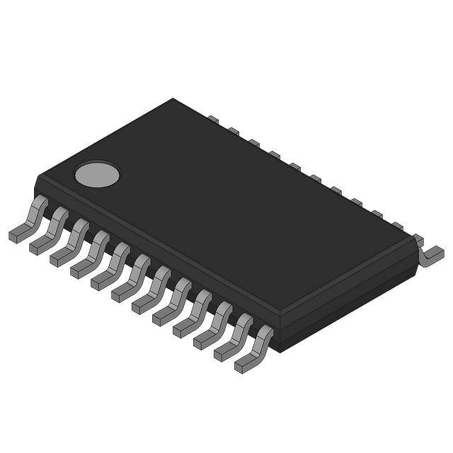
TSSOP24 (225mil)
GENERIC
MARKING DIAGRAM
XXXXXXXXXX
YMDDD
Specifications
Absolute Maximum Ratings at Ta = 25C
Parameter
Symbol
Supply voltage
VM max
Output peak current
IO peak
Output continuous current
Logic input voltage
(Note 1,3,4)
Conditions
Ratings
EMO pin input voltage
VEMO
Allowable power dissipation
Pd max
36
V
1.5
A
1.0
A
ST , IN1 , IN2 , EMM
-0.3 to +6
V
ORDERING INFORMATION
-0.3 to +6
V
1.4
W
Ordering Code:
LV8762T-TLM-H
LV8762T-MPB-H
Mounted on a specified
board. (Note 2)
Operating temperature
Topr
-20 to +85
C
Storage temperature
Tstg
-55 to +150
C
1. Stresses exceeding those listed in the Maximum Rating table may damage the device. If any of
these limits are exceeded, device functionality should not be assumed, damage may occur and
reliability may be affected.
2. Specified circuit board : 57mm57mm1.6mm, glass epoxy both-type board.
3. Absolute maximum ratings represent the value which cannot be exceeded for any length of time
4. Even when the device is used within the range of absolute maximum ratings, as a result of
continuous usage under high temperature, high current, high voltage, or drastic temperature
change, the reliability of the IC may be degraded. Please contact us for the further details
© Semiconductor Components Industries, LLC, 2017
May 2017- Rev. 2
XXXXX = Specific Device Code
Y = Year
M = Month
DDD = Additional Traceability Data
tw 10ms, duty 20%
IO max
VIN max
Unit
1
Package
TSSOP24 (225mil)
(Pb-Free / Halogen Free)
Shipping (Qty / packing)
2000 / Tape & Reel --- (TLM)
70 / Fan-Fold
--- (MPB)
† For information on tape and reel specifications, including part
orientation and tape sizes, please refer to our Tape and Reel
Packaging Specifications Brochure, BRD8011/D.
http://www.onsemi.com/pub_link/Collateral/BRD8011-D.PDF
Publication Order Number:
LV8762T/D
�LV8762T
Recommended Operating Ranges at Ta = 25C
Parameter
Supply voltage range
Symbol
(Note 5)
Conditions
Ratings
Unit
VM
9 to 32
V
VREF input voltage
VREF
0 to 3
V
Logic input voltage
VIN
0 to 5.5
V
ST , IN1 , IN2 , EMM
5. Functional operation above the stresses listed in the Recommended Operating Ranges is not implied. Extended exposure to stresses beyond the
Recommended Operating Ranges limits may affect device reliability.
Electrical Characteristics at Ta = 25°C, VM = 24 V, VREF = 1.5 V
Parameter
Symbol
(Note 6)
Conditions
Ratings
min
typ
Unit
max
General
Standby mode current drain
Operating mode current drain
REG5 output voltage
IMst
IM
VREG
Thermal shutdown temperature
Thermal hysteresis width
ST = “L”
ST = “H”, IN1 = “H”, IN2 = “L”, with no load
100
400
A
3
5
mA
IO = -1mA
4.5
5
5.5
V
TSD
Design guarantee (Note 7)
150
180
200
C
TSD
Design guarantee (Note 7)
C
40
Output block
Output on resistance
RonU
IO = 1A, upper side ON resistance
0.75
0.97
RonD
IO = -1A, under side ON resistance
0.5
0.65
Output leakage current
IOleak
VO = 32V
50
A
Diode forward voltage
VD
1.2
1.4
V
Rising time
tr
10% to 90%
ID = -1A
100
200
ns
Falling time
tf
90% to 10%
100
200
ns
tpLH
IN1 to OUTA, IN2 to OUTB (L H)
550
750
ns
tpHL
IN1 to OUTA, IN2 to OUTB (H L)
550
750
ns
High
VINH
ST , IN1 , IN2 , EMM
Low
VINL
Input output delay time
Control system input block
Logic input voltage
Logic pin input current 1
IINL
ST , IN1 , IN2 , EMM
2.0
5.5
V
0
0.8
V
4
8
12
A
30
50
70
A
IINH
VIN = 0.8V
VIN = 5V
VREF input current
IREF
VREF = 1.5V
-0.5
Current limit comparator
Vtlim
VREF = 1.5V
0.291
0.3
0.309
V
ICHOP
-6.5
-5
-3.5
A
VtCHOP
0.8
1
1.2
V
-32.5
-25
-17.5
A
1.2
1.5
1.8
V
27.7
28.7
29.7
V
250
550
s
90
125
155
kHz
0.4
V
-6.5
-5
-3.5
A
0.8
1
1.2
V
A
threshold voltage
CHOP pin charge current
CHOP pin threshold voltage
CMK pin charge current
CMK pin threshold voltage
ICMK
VtCMK
Charge pump block
Step-up voltage
VGH
VM = 24V
Rising time
tONG
VG = 0.1F
Oscillation frequency
Fcp
Short-circuit protection block
EMO output saturation voltage
SCP pin charge current
Comparator threshold voltage
VEMO
ISCP
IEMO = 1mA
SCP = 0V
VtSCP
6. Functional operation above the stresses listed in the Recommended Operating Ranges is not implied. Extended exposure to stresses beyond the
Recommended Operating Ranges limits may affect device reliability.
7. Design guarantee value and no measurement is made.
www.onsemi.com
2
�LV8762T
Package Dimensions
unit : mm
TSSOP24 4.4x6.5 / TSSOP24 (225 mil)
CASE 948BA
ISSUE A
SOLDERING FOOTPRINT*
5.80
1.0
(Unit: mm)
0.32
0.50
NOTE: The measurements are not to guarantee but for reference only.
*For additional information on our Pb−Free strategy and soldering
details, please download the ON Semiconductor Soldering and
Mounting Techniques Reference Manual, SOLDERRM/D.
www.onsemi.com
3
�LV8762T
Pin Assignment
24 EMO
PGND 2
23 CMK
OUTB 3
22 SCP
OUTB 4
21 CHOP
RNF 5
20 VREF
LV8762T
EMM 1
RNF 6
VM 7
VM 8
19 IN2
18 IN1
17 REG5
OUTA 9
16 CP1
OUTA 10
15 CP2
NC 11
14 VG
ST 12
13 GND
Top view
Pd max - Ta
Allowable power dissipation, Pd max - W
2.0
1.5
1.40
1.0
0.73
0.5
0
—20
0
20
40
60
Ambient temperature, Ta -
www.onsemi.com
4
80
C
100
�LV8762T
Substrate Specifications (Substrate recommended for operation of LV8762T)
Size
: 57mm × 57mm × 1.6mm (two-layer substrate)
Material
: Glass epoxy both-type board
L1 : Copper wiring pattern diagram
L2 : Copper wiring pattern diagram
Cautions
1) For the set design, employ the derating design with sufficient margin.
Stresses to be derated include the voltage, current, junction temperature, power loss, and mechanical stresses such as
vibration, impact, and tension.
Accordingly, the design must ensure these stresses to be as low or small as possible.
The guideline for ordinary derating is shown below :
(1)Maximum value 80% or less for the voltage rating
(2)Maximum value 80% or less for the current rating
(3)Maximum value 80% or less for the temperature rating
2) After the set design, be sure to verify the design with the actual product.
Confirm the solder joint state and verify also the reliability of solder joint for the Exposed Die-Pad, etc.
Any void or deterioration, if observed in the solder joint of these parts, causes deteriorated thermal conduction, possibly
resulting in thermal destruction of IC.
www.onsemi.com
5
�GND
REG5
ST
VG
www.onsemi.com
6
LVS
TSD
Oscillation
circuit
Reference
Voltage
Circuit
Charge pump
CP1 CP2
Output preamplifier stage
+ -
CHOP
Output control
logic
OUTB
EMM IN1 IN2
OUTA
RNF
CMK
Current Limiter
Mask
Current
Limiter
Circuit
Output preamplifier stage
SCP
Short-circuit
Protection Circuit
Brake-Time
Setting Circuit
VM
M
+
+
VREF
EMO
PGND
LV8762T
Block Diagram
�LV8762T
Pin Functions
Pin No.
Pin Name
Pin Functtion
18
IN1
Output control signal input pin 1.
19
IN2
Output control signal input pin 2.
1
EMM
Short protection mode setting.
Equivalent Circuit
VREG5
19 18 1
GND
12
ST
Standby mode setting
VREG5
12
GND
9, 10
OUTA
OUTA output pin.
3, 4
OUTB
OUTB output pin.
7, 8
VM
Motor power-supply connection pin.
5, 6
RNF
Current sense resistor connection pin.
PGND
Power ground.
2
7 8
9 10
3 4
2
5 6
GND
14
VG
Charge pump capacitor connection pin.
8
VM
Motor power-supply connection pin.
16
CP1
Charge pump capacitor connection pin.
15
CP2
Charge pump capacitor connection pin.
VREG5
16
8
15
14
GND
Continued on next page.
www.onsemi.com
7
�LV8762T
Continued from preceding page.
Pin No.
20
Pin Name
VREF
Pin Functtion
Equivalent Circuit
Reference voltage input pin for output
VREG5
current limit setting.
20
GND
17
REG5
Internal reference voltage output pin.
VM
17
GND
24
EMO
Alert signal output
VREG5
24
GND
21
CHOP
Capacitor connection for current limit
VREG5
break time setting
22
SCP
Capacitor connection for short detection
time setting
GND
21 22
Continued on next page.
www.onsemi.com
8
�LV8762T
Continued from preceding page.
Pin No.
23
Pin Name
CMK
Pin Functtion
Capacitor connection for current limit
mask setting
Equivalent Circuit
VREG5
23
GND
www.onsemi.com
9
�LV8762T
Description of operation
1.Input Pin Function
Each input terminal has the function to prevent the flow of the current from an input to a power supply.
Therefore, Even if a power supply (VM) is turned off in the state that applied voltage to an input terminal, the electric
current does not flow into the power supply.
1-1) Chip enable function
This IC is switched between standby and operating mode by setting the ST pin. In standby mode, the IC is set to
power-save mode and all logic is reset. In addition, the internal regulator circuit and charge pump circuit do not operate
in standby mode.
ST
mode
Internal regulator
“L” or OPEN
Standby mode
standby
Charge pump
standby
“H”
Operation mode
operation
operation
1-2)DCM output control logic
Contol Input
Output
Mode
ST
IN1
IN2
OUTA
OUTB
L
*
*
OFF
OFF
H
L
L
OFF
OFF
Output OFF
H
H
L
H
L
CW (forward)
H
L
H
L
H
CCW (reverse)
H
H
H
L
L
Brake
1-3)Current limit control timing chart
LIMIT current
Output
current
OUTA
Tchop
OUTB
CHARGE
SLOW
www.onsemi.com
10
Standby
�LV8762T
1-4) Setting the time of current limit brake value
This IC can set the time of the current limit break by connecting the capacitor with CHOP-GND.
The value of the capacitor is decided according to the following expression.
brake time: TCHOP ≈ CCHOP × VtCHOP ÷ ICHOP [sec]
VtCHOP:CHOP comparator threshold voltage. TYP = 1.0 [V]
ICHOP:CHOP charge current. TYP = 5 [A]
ex. Cchop = 50[pF]
Tchop[sec] = 50[pF] × 1.0[V] ÷ 5[A] = 10[s]
1-5)Setting the current limit value
The current limit value of the DCM driver is determined by the VREF voltage and the resistance (RNF) connected across
the RNF and GND pins using the following formula :
Ilimit [A] ≈ (VREF [V] ÷ 5) ÷ RNF [])
Assuming VREF = 1.5V, RNF = 1, the current limit is :
Ilimit = 1.5V ÷ 5 ÷ 1 = 0.3 A
1-6) Setting the mask of current limit
CMK
mask of current limit
“L”
no operation
“H” or OPEN
operation
This function can be switched by CMK pin.
This function can prevent the current limit from working by the motor start-up current when the current limit value is set
low.
1-7) Setting the time of the mask of current limit
This IC can set the time of the mask of current limit by connection the capacitor with CMK-GND.
The value of the capacitor is decided according to the following expression.
Time of mask:TCMK ≈ CCMK × VtCMK ÷ ICMK [sec]
VtCMK:CMK comparator threshold voltage. TYP = 1.0 [V]
ICMK:CMK charge current. TYP = 25 [A]
ex. CCMK = 0.1 [F]
TCMK[sec] = 0.1 [F] × 1.5 [V] ÷ 25 [A] = 6[ms]
2.Output short-circuit protection function
Thils IC incorporates an output short-circuit protection circuit.It turns the output off to prevent destruction of the IC if a
problem such as an output pin being shorted to the motor power supply or ground occurs.
Then short-circuit detected, alart signal is assert to EMO pin.
2-1) Output short protect mode
This function can be switched by EMM pin. EMM pin is L or OPEN then latch method, H then auto-retry method.
EMM Pin
Method
“L” or OPEN
Latch
“H”
Auto retry
www.onsemi.com
11
�LV8762T
2-2) Protection function operation (Latch method)
The short-circuit protection circuit is activated when it detects the output short-circuit state. If the short-circuit state
continues for the internally preset period ( 2 s), the protection circuit turns off the output from which the short-circuit
state has been detected. Then it turns the output on again after a lapse of the timer latch time (TSCP) described later. If the
short-circuit state is still detected, it changes all the outputs to the standby mode and retains the state. The latched state is
released by setting the ST to L.
Output ON
H bridge
Output state
Output ON
Stand-by
state
Outout OFF
Threshold voltage
SCP voltage
Short-circuit
detection state
Shortcircuit
Release
Short-circuit
Internal counter
1st counter
start
1st counter
stop
1st counter
start
1st counter
end
2st counter
start
2st counter
end
2-3) Protection function operation (Auto retry method)
In this mode, short-protection function try repeatedly to detecting short-circuit.
The short-circuit detection circuit operates when a short output is detected as well as the latch method. The output is
switched to the standby mode when the operation of the short-circuit detection circuit exceeds time (TSCP) of the timer
latch, and it returns to the turning on mode again after 2 ms (typ). At this time, the switching mode is repeated when is still
in the overcurrent mode until the overcurrent mode is made clear.
2-4)Unusual Condition Warning Output Pin (EMO)
The LV8762T is provided with the EMO pin which notifies the CPU of an unusual condition if the protection circuit
operates by detecting an abnormal condition of the IC. This pin is of the open-drain output type, and if abnormality is
detected, the EMO output becomes (EMO=L) of on.
The EMO pin is placed in the ON state when one of the following conditions occurs.
1. Shorting-to-power or shorting-to-ground occurs at the output pin and the output short-circuit protection circuit is
activated.
2. The IC junction temperature rises and the thermal protection circuit is activated.
2-5)Timer latch-up (TSCP)
The user can set the time at which the outputs are turned off when a short-circuit occurs by connecting a capacitor (CSCP)
across the SCP and GND pins. The value of the capacitor (CSCP) can be determined by the following formula :
Timer latch-up : TSCP
TSCP CSCP × VtSCP ÷ ISCP [sec]
VtSCP : Comparator threshold voltage (1 V typical)
ISCP : SCP charge current (5 A typical)
www.onsemi.com
12
�LV8762T
3.Thermal shutdown function
The thermal shutdown circuit is included, and the output is turned off when junction temperature Tj exceeds 180C, and
the abnormal state warning output(EMO pin) is turned on at the same time.
When the temperature falls hysteresis level, output is driven again (automatic restoration) The thermal shutdown circuit
doesn’t guarantee protection of the set and the destruction prevention because it works at the temperature that is higher
than rating (Tjmax = 150C) of the junction temperature
TSD=180C (typ)
ΔTSD=40C (typ)
4.Charge pump Circuit
When the ST pin is set High, the charge pump circuit operates and the VG pin voltage is boosted from the VM voltage to
the VM+VREG5 voltage.
If the VG pin voltage is not boosted to VM + 4 V or more, the output pin cannot be turned on. Therefore it is recommended
that the drive of the motor is started after the time has passed tONG or more.
ST
VG pin voltage
VM+VREG5
VM+4V
VM
tONG
www.onsemi.com
13
�LV8762T
5.Application Circuit Example
Control input
1 EMM
EMO 24
2 PGND
CMK 23
3 OUTB
SCP 22
4 OUTB
CHOP 21
Overcurrent detection
monitor pin
0.1 F
50pF
5 RNF
VREF 20
LV8762T
6 RNF
M
7 VM
- +
Control input
8 VM
IN2 19
Control input
IN1 18
REG5 17
9 OUTA
CP1 16
10 OUTA
CP2 15
11 NC
VG 14
12 ST
GND 13
Current limit value
When VREF = 1.5 V,
Ilimit = Vref ÷ 5 ÷ RNF
= 1.5 V ÷ 5 ÷ 1 = 0.3 A
Setting the current limit regeneration time and short-circuit detection time
TSCP CSCP VtSCP ÷ ISCP
= 50 pF 1 V ÷ 5 A = 10 s
Setting at current limit mask time
TCMK ≈ CCMK × VtCMK ÷ ICMK
= 0.1 F 1.5 V ÷ 25 A = 6 ms
Setting at current limit brake time
TCHOP ≈ CCHOP × VtCHOP ÷ ICHOP
= 50 pF × 1 V ÷ 5 A = 10 s
* The external part constant is a reference value.
www.onsemi.com
14
50pF
Output current
setting input
�LV8762T
ON Semiconductor and the ON Semiconductor logo are trademarks of Semiconductor Components Industries, LLC dba ON Semiconductor or its subsidiaries
in the United States and/or other countries. ON Semiconductor owns the rights to a number of patents, trademarks, copyrights, trade secrets, and other
intellectual property. A listing of ON Semiconductor’s product/patent coverage may be accessed at www.onsemi.com/site/pdf/Patent-Marking.pdf. ON
Semiconductor reserves the right to make changes without further notice to any products herein. ON Semiconductor makes no warranty, representation or
guarantee regarding the suitability of its products for any particular purpose, nor does ON Semiconductor assume any liability arising out of the application or
use of any product or circuit, and specifically disclaims any and all liability, including without limitation special, consequential or incidental damages. Buyer is
responsible for its products and applications using ON Semiconductor products, including compliance with all laws, regulations and safety requirements or
standards, regardless of any support or applications information provided by ON Semiconductor. “Typical” parameters which may be provided in ON
Semiconductor data sheets and/or specifications can and do vary in different applications and actual performance may vary over time. All operating parameters,
including “Typicals” must be validated for each customer application by customer’s technical experts. ON Semiconductor does not convey any license under its
patent rights nor the rights of others. ON Semiconductor products are not designed, intended, or authorized for use as a critical component in life support
systems or any FDA Class 3 medical devices or medical devices with a same or similar classification in a foreign jurisdiction or any devices intended for
implantation in the human body. Should Buyer purchase or use ON Semiconductor products for any such unintended or unauthorized application, Buyer shall
indemnify and hold ON Semiconductor and its officers, employees, subsidiaries, affiliates, and distributors harmless against all claims, costs, damages, and
expenses, and reasonable attorney fees arising out of, directly or indirectly, any claim of personal injury or death associated with such unintended or
unauthorized use, even if such claim alleges that ON Semiconductor was negligent regarding the design or manufacture of the part. ON Semiconductor is an
Equal Opportunity/Affirmative Action Employer. This literature is subject to all applicable copyright laws and is not for resale in any manner.
www.onsemi.com
15
�