5 V ECL 3‐Bit Differential
Flip‐Flop
MC10E431
Description
The MC10E431 is a 3-bit flip-flop with differential clock, data input
and data output.
The asynchronous Set and Reset controls are edge-triggered rather
than level controlled. This allows the user to rapidly set or reset the
flip-flop and then continue clocking at the next clock edge, without the
necessity of de-asserting the set/reset signal (as would be the case with
a level controlled set/reset).
The E431 is also designed with larger internal swings, an approach
intended to minimize the time spent crossing the threshold region and
thus reduce the metastability susceptibility window.
The differential input structures are clamped so that the inputs of
unused registers can be left open without upsetting the bias network of
the device. The clamping action will assert the D and the CLK sides of
the inputs. Because of the edge triggered flip-flop nature of the device
simultaneously opening both the clock and data inputs will result in an
output which reaches an unidentified but valid state. Note that the
input clamps only operate when both inputs fall to 2.5 V below VCC.
The VBB pin, an internally generated voltage supply, is available to
this device only. For single-ended input conditions, the unused
differential input is connected to VBB as a switching reference voltage.
VBB may also rebias AC coupled inputs. When used, decouple VBB
and VCC via a 0.01 mF capacitor and limit current sourcing or sinking
to 0.5 mA. When not used, VBB should be left open.
Features
•
•
•
•
•
•
•
•
•
•
•
•
Edge-Triggered Asynchronous Set and Reset
Differential D, CLK and Q; VBB Reference Available
1100 MHz Min. Toggle Frequency
PECL Mode Operating Range: VCC = 4.2 V to 5.7 V
with VEE = 0 V
NECL Mode Operating Range: VCC = 0 V
with VEE = −4.2 V to −5.7 V
Internal Input 50 kW Pulldown Resistors
ESD Protection:
♦ > 2 kV Human Body Model
♦ > 200 V Machine Model
♦ > 2 kV Charged Device Model
Meets or Exceeds JEDEC Spec EIA/JESD78 IC
Latchup Test
Moisture Sensitivity: Level 3 (Pb-Free)
(For Additional Information, see Application Note AND8003/D)
Flammability Rating: UL 94 V−0 @ 0.125 in,
Oxygen Index: 28 to 34
Transistor Count = 348 Devices
These Devices are Pb-Free, Halogen Free and are RoHS Compliant
© Semiconductor Components Industries, LLC, 2016
April, 2021 − Rev. 12
1
www.onsemi.com
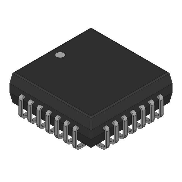
PLCC−28
FN SUFFIX
CASE 776−02
MARKING DIAGRAM*
1 28
MC10E431FNG
AWLYYWW
A
WL
YY
WW
G
= Assembly Location
= Wafer Lot
= Year
= Work Week
= Pb-Free Package
*For additional marking information, refer to
Application Note AND8002/D.
ORDERING INFORMATION
Device
Package
Shipping†
MC10E431FNG
PLCC−28
(Pb-Free)
37 Units / Tube
MC10E431FNR2G
PLCC−28
(Pb-Free)
500
Tape & Reel
†For information on tape and reel specifications, including part orientation and tape sizes, please refer
to our Tape and Reel Packaging Specifications
Brochure, BRD8011/D.
Publication Order Number:
MC10E431/D
�MC10E431
VBB
CLK2 CLK2
25
24
23
D2
D2
R2
S2
22
21
20
19
Table 1. PIN DESCRIPTION
PIN
FUNCTION
CLK1
26
18
Q2
D[0:2], D[0:2]
ECL Differential Data Inputs
CLK1
27
17
Q2
CLK[0:2], CLK[0:2]
ECL Differential Clock
R1
16
VCC
S[0:2]
ECL Edge Triggered Set Inputs
28
R[0:2]
ECL Edge Triggered Reset Input
1
15
Q1
Q[0:2], Q[0:2]
ECL Differential Data Outputs
Q1
VBB
Reference Voltage Output
VCC, VCCO
Positive Supply
VEE
Negative Supply
VEE
MC10E431
S1
2
14
D1
3
13
Q0
D1
4
12
Q0
5
6
7
CLK0 CLK0 D0
8
9
10
D0
R0
S0
11
VCCO
* All VCC and VCCO pins are tied together on the die.
Warning: All VCC, VCCO, and VEE pins must be externally connected to Power Supply to guarantee proper operation.
Figure 1. Pinout: PLCC-28 (Top View)
S0
D0
D0
D
CLK0
CLK0
R0
S1
D1
D1
S
R
D
CLK1
CLK1
S
R
Q
Q0
Q
Q0
Q
Q1
Q
Q1
Q
Q2
Q
Q2
Table 2. FUNCTION TABLE
Dn
CLKn
Rn
Sn
L
Z
L
L
L
H
Z
L
L
H
X
X
Z
L
L
X
X
L
Z
H
Z = Low to high transition
X = Don’t Care
R1
S2
D2
D2
D
CLK2
CLK2
S
R
R2
VBB
Figure 2. Logic Diagram
www.onsemi.com
2
Qn
�MC10E431
Table 3. MAXIMUM RATINGS
Symbol
Parameter
Condition 1
VCC
PECL Mode Power Supply
VEE = 0 V
VI
PECL Mode Input Voltage
NECL Mode Input Voltage
VEE = 0 V
VCC = 0 V
Iout
Output Current
Continuous
Surge
IBB
VBB Sink/Source
TA
Operating Temperature Range
Tstg
Storage Temperature Range
qJA
Thermal Resistance (Junction-to-Ambient)
0 lfpm
500 lfpm
qJC
Thermal Resistance (Junction-to-Case)
Standard Board
Tsol
Wave Solder (Pb-Free)
Condition 2
Rating
Unit
8
V
6
−6
V
50
100
mA
±0.5
mA
0 to +85
°C
−65 to +150
°C
PLCC−28
PLCC−28
63.5
43.5
°C/W
PLCC−28
22 to 26
°C/W
265
°C
VI v VCC
VI w VEE
Stresses exceeding those listed in the Maximum Ratings table may damage the device. If any of these limits are exceeded, device functionality
should not be assumed, damage may occur and reliability may be affected.
Table 4. 10E SERIES PECL DC CHARACTERISTICS (VCCx= 5.0 V; VEE= 0.0 V (Note 1))
0°C
Symbol
Characteristic
Min
25°C
Typ
Max
110
132
Min
85°C
Typ
Max
110
132
Min
Typ
Max
Unit
110
132
mA
IEE
Power Supply Current
VOH
Output HIGH Voltage (Note 2)
3980
4070
4160
4020
4105
4190
4090
4185
4280
mV
VOL
Output LOW Voltage (Note 2)
3050
3210
3370
3050
3210
3370
3050
3227
3405
mV
VIH
Input HIGH Voltage (Single-Ended)
3830
3995
4160
3870
4030
4190
3940
4110
4280
mV
VIL
Input LOW Voltage (Single-Ended)
3050
3285
3520
3050
3285
3520
3050
3302
3555
mV
VBB
Output Voltage Reference
3.62
3.74
3.65
3.75
3.69
3.81
V
Input HIGH Voltage Common Mode
Range (Differential Configuration) (Note 3)
2.7
5.0
2.7
5.0
2.7
5.0
V
150
mA
VIHCMR
IIH
Input HIGH Current
IIL
Input LOW Current
150
0.5
0.3
150
0.5
0.25
0.3
0.2
mA
NOTE: Device will meet the specifications after thermal equilibrium has been established when mounted in a test socket or printed circuit
board with maintained transverse airflow greater than 500 lfpm.
1. Input and output parameters vary 1:1 with VCC. VEE can vary −0.46 V / +0.06 V.
2. Outputs are terminated through a 50 W resistor to VCC − 2.0 V.
3. VIHCMR min varies 1:1 with VEE, max varies 1:1 with VCC.
www.onsemi.com
3
�MC10E431
Table 5. 10E SERIES NECL DC CHARACTERISTICS (VCCx= 0.0 V; VEE= −5.0 V (Note 1)
0°C
Symbol
Characteristic
Min
25°C
Typ
Max
110
132
Min
85°C
Typ
Max
110
132
Min
Typ
Max
Unit
110
132
mA
IEE
Power Supply Current
VOH
Output HIGH Voltage (Note 2)
−1020
−930
−840
−980
−895
−810
−910
−815
−720
mV
VOL
Output LOW Voltage (Note 2)
−1950
−1790
−1630
−1950
−1790
−1630
−1950
−1773
−1595
mV
VIH
Input HIGH Voltage (Single-Ended)
−1170
−1005
−840
−1130
−970
−810
−1060
−890
−720
mV
VIL
Input LOW Voltage (Single-Ended)
−1950
−1715
−1480
−1950
−1715
−1480
−1950
−1698
−1445
mV
VBB
Output Voltage Reference
−1.38
−1.27
−1.35
−1.25
−1.31
−1.19
V
Input HIGH Voltage Common Mode
Range (Differential Configuration) (Note 3)
−2.3
0.0
−2.3
0.0
−2.3
0.0
V
150
mA
VIHCMR
IIH
Input HIGH Current
IIL
Input LOW Current
150
0.5
0.3
150
0.5
0.065
0.3
0.2
mA
NOTE: Device will meet the specifications after thermal equilibrium has been established when mounted in a test socket or printed circuit
board with maintained transverse airflow greater than 500 lfpm.
1. Input and output parameters vary 1:1 with VCC. VEE can vary −0.46 V / +0.06 V.
2. Outputs are terminated through a 50 W resistor to VCC − 2.0 V.
3. VIHCMR min varies 1:1 with VEE, max varies 1:1 with VCC.
Table 6. AC CHARACTERISTICS (VCCx= 5.0 V; VEE= 0.0 V or VCCx= 0.0 V; VEE= −5.0 V (Note 1))
−40°C
Min
Characteristic
Symbol
Typ
fMAX
Maximum Toggle Frequency
tPLH
tPHL
Propagation Delay to Output
CLK
R
S
550
500
500
700
725
725
tS
Setup Time
D
R (Note 2)
S (Note 2)
250
1100
1100
tH
Hold Time
D
250
CLK
400
tPW
Minimum Pulse Width
tskew
25°C
Max
Min
Typ
85°C
Max
Min
Typ
Max
1.1
850
975
975
550
550
550
700
725
725
0
700
700
200
1000
1000
0
200
GHz
850
925
925
550
550
550
700
725
725
0
700
700
200
1000
1000
0
700
700
0
200
0
400
Within-Device Skew (Note 3)
50
tJITTER
Random Clock Jitter (RMS)
很抱歉,暂时无法提供与“MC10E431FNR2G”相匹配的价格&库存,您可以联系我们找货
免费人工找货