MC14001UB, MC14011UB
UB−Suffix Series
CMOS Gates
The UB Series logic gates are constructed with P and N channel
enhancement mode devices in a single monolithic structure
(Complementary MOS). Their primary use is where low power
dissipation and/or high noise immunity is desired. The UB set of
CMOS gates are inverting non−buffered functions.
http://onsemi.com
MARKING
DIAGRAMS
Features
• Supply Voltage Range = 3.0 Vdc to 18 Vdc
• Linear and Oscillator Applications
• Capable of Driving Two Low−Power TTL Loads or One
•
•
•
14
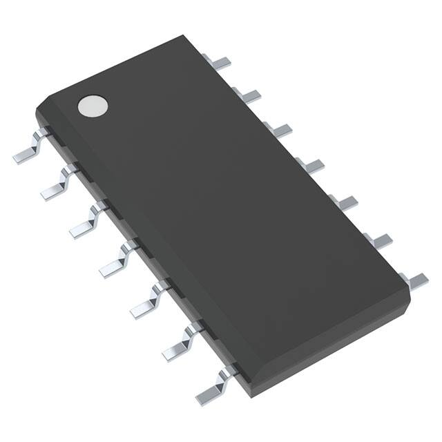
PDIP−14
P SUFFIX
CASE 646
Low−Power Schottky TTL Load Over the Rated Temperature Range
Double Diode Protection on All Inputs
Pin−for−Pin Replacements for Corresponding CD4000 Series UB
Suffix Devices
Pb−Free Packages are Available
1
14
SOIC−14
D SUFFIX
CASE 751A
MAXIMUM RATINGS (Voltages Referenced to VSS)
Symbol
140xxUG
AWLYWW
1
Value
Unit
−0.5 to +18.0
V
−0.5 to VDD + 0.5
V
Input or Output Current
(DC or Transient) per Pin
± 10
mA
PD
Power Dissipation, per Package
(Note 1)
500
mW
TA
Ambient Temperature Range
−55 to +125
°C
ORDERING INFORMATION
Tstg
Storage Temperature Range
−65 to +150
°C
TL
Lead Temperature
(8−Second Soldering)
260
°C
See detailed ordering and shipping information in the package
dimensions section on page 4 of this data sheet.
VDD
Vin, Vout
Iin, Iout
Parameter
MC140xxUBCP
AWLYYWWG
DC Supply Voltage Range
Input or Output Voltage Range
(DC or Transient)
xx
A
WL, L
YY, Y
WW, W
G
= Specific Device Code
= Assembly Location
= Wafer Lot
= Year
= Work Week
= Pb−Free Package
Stresses exceeding Maximum Ratings may damage the device. Maximum
Ratings are stress ratings only. Functional operation above the Recommended
Operating Conditions is not implied. Extended exposure to stresses above the
Recommended Operating Conditions may affect device reliability.
1. Temperature Derating:
Plastic “P and D/DW” Packages: – 7.0 mW/_C From 65_C To 125_C
This device contains protection circuitry to guard against damage due to high
static voltages or electric fields. However, precautions must be taken to avoid
applications of any voltage higher than maximum rated voltages to this
high−impedance circuit. For proper operation, Vin and Vout should be constrained
to the range VSS v (Vin or Vout) v VDD.
Unused inputs must always be tied to an appropriate logic voltage level
(e.g., either VSS or VDD). Unused outputs must be left open.
© Semiconductor Components Industries, LLC, 2006
October, 2006 − Rev. 6
1
Publication Order Number:
MC14001UB/D
�MC14001UB, MC14011UB
LOGIC DIAGRAMS
MC14001UB
Quad 2−Input
NOR Gate
1
2
5
6
8
9
12
13
MC14011UB
Quad 2−Input
NAND Gate
1
3
3
2
5
4
4
6
8
10
10
9
12
11
11
13
VDD = PIN 14
VSS = PIN 7
FOR ALL DEVICES
PIN ASSIGNMENTS
MC14001UB
Quad 2−Input NOR Gate
MC14011UB
Quad 2−Input NAND Gate
IN 1A
1
14
VDD
IN 1A
1
14
VDD
IN 2A
2
13
IN 2D
IN 2A
2
13
IN 2D
OUTA
3
12
IN 1D
OUTA
3
12
IN 1D
OUTB
4
11
OUTD
OUTB
4
11
OUTD
IN 1B
5
10
OUTC
IN 1B
5
10
OUTC
IN 2B
6
9
IN 2C
IN 2B
6
9
IN 2C
VSS
7
8
IN 1C
VSS
7
8
IN 1C
http://onsemi.com
2
�MC14001UB, MC14011UB
ÎÎÎÎÎÎÎÎÎÎÎÎÎÎÎÎÎÎÎÎÎÎÎÎÎÎÎÎÎÎÎÎÎ
ÎÎÎÎÎÎÎÎÎÎ
ÎÎÎÎ
ÎÎÎ
ÎÎÎÎÎ
ÎÎÎÎÎÎÎÎÎ
ÎÎÎÎÎ
ÎÎÎ
ÎÎÎÎÎÎÎÎÎÎÎÎÎÎÎÎÎÎÎÎÎÎÎÎÎÎÎÎÎÎÎÎÎ
ÎÎÎÎÎÎÎÎÎÎ
ÎÎÎÎ
ÎÎÎ
ÎÎÎÎÎ
ÎÎÎÎÎÎÎÎÎ
ÎÎÎÎÎ
ÎÎÎ
ÎÎÎ
ÎÎÎ
ÎÎÎÎ
ÎÎÎÎÎÎÎ
ÎÎÎ
ÎÎÎ
ÎÎÎÎÎÎÎÎÎÎ
ÎÎÎÎ
ÎÎÎ
ÎÎÎ
ÎÎÎ
ÎÎÎÎ
ÎÎÎÎ
ÎÎÎ
ÎÎÎ
ÎÎÎ
ÎÎÎ
ÎÎÎÎÎÎÎÎÎÎ
ÎÎÎÎ
ÎÎÎ
ÎÎÎ
ÎÎÎ
ÎÎÎÎ
ÎÎÎÎ
ÎÎÎ
ÎÎÎ
ÎÎÎ
ÎÎÎ
ÎÎÎÎÎÎÎÎÎÎ
ÎÎÎÎ
ÎÎÎ
ÎÎÎ
ÎÎÎ
ÎÎÎÎ
ÎÎÎÎ
ÎÎÎ
ÎÎÎ
ÎÎÎ
ÎÎÎ
ÎÎÎÎÎÎÎÎÎÎ
ÎÎÎÎ
ÎÎÎ
ÎÎÎ
ÎÎÎ
ÎÎÎÎ
ÎÎÎÎÎÎÎ
ÎÎÎ
ÎÎÎ
ÎÎÎ
ÎÎÎÎÎÎÎÎÎÎ
ÎÎÎÎ
ÎÎÎ
ÎÎÎ
ÎÎÎ
ÎÎÎÎ
ÎÎÎÎ
ÎÎÎ
ÎÎÎ
ÎÎÎ
ÎÎÎ
ÎÎÎÎÎÎÎÎÎÎ
ÎÎÎ
ÎÎÎ
ÎÎÎÎ
ÎÎÎ
ÎÎÎ
ÎÎÎ
ÎÎÎÎ
ÎÎÎ
ÎÎÎÎ
ÎÎÎ
ÎÎÎÎÎÎÎÎÎÎ
ÎÎÎÎ
ÎÎÎ
ÎÎÎ
ÎÎÎ
ÎÎÎÎ
ÎÎÎÎ
ÎÎÎ
ÎÎÎ
ÎÎÎ
ÎÎÎ
ÎÎÎÎÎÎÎÎÎÎ
ÎÎÎÎ
ÎÎÎ
ÎÎÎ
ÎÎÎ
ÎÎÎÎ
ÎÎÎÎ
ÎÎÎ
ÎÎÎ
ÎÎÎ
ÎÎÎ
ÎÎÎÎÎÎÎÎÎÎ
ÎÎÎ
ÎÎÎ
ÎÎÎÎ
ÎÎÎ
ÎÎÎ
ÎÎÎ
ÎÎÎÎ
ÎÎÎ
ÎÎÎÎ
ÎÎÎ
ÎÎÎÎÎÎÎÎÎÎ
ÎÎÎÎ
ÎÎÎ
ÎÎÎ
ÎÎÎ
ÎÎÎÎ
ÎÎÎÎ
ÎÎÎ
ÎÎÎ
ÎÎÎ
ÎÎÎ
ÎÎÎÎ
ÎÎÎ
ÎÎÎÎ
ÎÎÎ
ÎÎÎÎÎÎÎÎÎÎ
ÎÎÎ
ÎÎÎ
ÎÎÎÎ
ÎÎÎ
ÎÎÎ
ÎÎÎ
ÎÎÎÎÎÎÎÎÎÎ
ÎÎÎÎ
ÎÎÎ
ÎÎÎ
ÎÎÎ
ÎÎÎÎ
ÎÎÎÎ
ÎÎÎ
ÎÎÎ
ÎÎÎ
ÎÎÎ
ÎÎÎÎÎÎÎÎÎÎ
ÎÎÎÎ
ÎÎÎ
ÎÎÎ
ÎÎÎ
ÎÎÎÎ
ÎÎÎÎ
ÎÎÎ
ÎÎÎ
ÎÎÎ
ÎÎÎ
ÎÎÎÎÎÎÎÎÎÎ
ÎÎÎÎ
ÎÎÎ
ÎÎÎ
ÎÎÎ
ÎÎÎÎ
ÎÎÎÎ
ÎÎÎ
ÎÎÎ
ÎÎÎ
ÎÎÎ
ÎÎÎÎÎÎÎÎÎÎ
ÎÎÎÎ
ÎÎÎ
ÎÎÎ
ÎÎÎ
ÎÎÎÎ
ÎÎÎÎ
ÎÎÎ
ÎÎÎ
ÎÎÎ
ÎÎÎ
ÎÎÎÎÎÎÎÎÎÎ
ÎÎÎÎ
ÎÎÎ
ÎÎÎ
ÎÎÎ
ÎÎÎÎ
ÎÎÎÎ
ÎÎÎ
ÎÎÎ
ÎÎÎ
ÎÎÎ
ÎÎÎÎÎÎÎÎÎÎ
ÎÎÎ
ÎÎÎ
ÎÎÎÎ
ÎÎÎ
ÎÎÎ
ÎÎÎ
ÎÎÎÎ
ÎÎÎ
ÎÎÎÎ
ÎÎÎ
ÎÎÎÎÎÎÎÎÎÎ
ÎÎÎÎ
ÎÎÎ
ÎÎÎ
ÎÎÎ
ÎÎÎÎ
ÎÎÎÎ
ÎÎÎ
ÎÎÎ
ÎÎÎ
ÎÎÎ
ÎÎÎÎÎÎÎÎÎÎ
ÎÎÎÎ
ÎÎÎ
ÎÎÎ
ÎÎÎ
ÎÎÎÎ
ÎÎÎÎ
ÎÎÎ
ÎÎÎ
ÎÎÎ
ÎÎÎ
ÎÎÎÎÎÎÎÎÎÎ
ÎÎÎ
ÎÎÎ
ÎÎÎÎ
ÎÎÎ
ÎÎÎ
ÎÎÎ
ÎÎÎÎ
ÎÎÎ
ÎÎÎÎ
ÎÎÎ
ÎÎÎÎÎÎÎÎÎÎ
ÎÎÎÎ
ÎÎÎ
ÎÎÎ
ÎÎÎ
ÎÎÎÎ
ÎÎÎÎ
ÎÎÎ
ÎÎÎ
ÎÎÎ
ÎÎÎ
ÎÎÎÎÎÎÎÎÎÎ
ÎÎÎÎ
ÎÎÎ
ÎÎÎ
ÎÎÎÎÎÎÎÎÎÎÎÎÎÎÎÎÎ
ÎÎÎ
ÎÎÎÎ
ÎÎÎÎ
ÎÎÎ
ÎÎÎ
ÎÎÎ
ÎÎÎ
ÎÎÎÎÎÎÎÎÎÎ
ÎÎÎÎ
ÎÎÎ
ÎÎÎÎÎÎÎÎÎÎÎÎÎÎÎÎÎ
ÎÎÎ
ÎÎÎÎÎÎÎÎÎÎ
ÎÎÎÎ
ÎÎÎ
ÎÎÎÎÎÎÎÎÎÎÎÎÎÎÎÎÎ
ÎÎÎ
ÎÎÎÎÎÎÎÎÎÎ
ÎÎÎÎ
ÎÎÎ
ÎÎÎÎÎÎÎÎÎÎÎÎÎÎÎÎÎ
ÎÎÎ
ELECTRICAL CHARACTERISTICS (Voltages Referenced to VSS)
Characteristic
Symbol
− 55_C
25_C
125_C
VDD
Vdc
Min
Max
Min
Typ
(Note 2)
Max
Min
Max
Unit
Output Voltage
Vin = VDD or 0
“0” Level
VOL
5.0
10
15
−
−
−
0.05
0.05
0.05
−
−
−
0
0
0
0.05
0.05
0.05
−
−
−
0.05
0.05
0.05
Vdc
Vin = 0 or VDD
“1” Level
VOH
5.0
10
15
4.95
9.95
14.95
−
−
−
4.95
9.95
14.95
5.0
10
15
−
−
−
4.95
9.95
14.95
−
−
−
Vdc
“0” Level
VIL
5.0
10
15
−
−
−
1.0
2.0
2.5
−
−
−
2.25
4.50
6.75
1.0
2.0
2.5
−
−
−
1.0
2.0
2.5
5.0
10
15
4.0
8.0
12.5
−
−
−
4.0
8.0
12.5
2.75
5.50
8.25
−
−
−
4.0
8.0
12.5
−
−
−
5.0
5.0
10
15
– 1.2
– 0.25
– 0.62
– 1.8
−
−
−
−
– 1.0
– 0.2
– 0.5
– 1.5
– 1.7
– 0.36
– 0.9
– 3.5
−
−
−
−
– 0.7
– 0.14
– 0.35
– 1.1
−
−
−
−
IOL
5.0
10
15
0.64
1.6
4.2
−
−
−
0.51
1.3
3.4
0.88
2.25
8.8
−
−
−
0.36
0.9
2.4
−
−
−
mAdc
Input Current
Iin
15
−
± 0.1
−
± 0.00001
± 0.1
−
± 1.0
mAdc
Input Capacitance
(Vin = 0)
Cin
−
−
−
−
5.0
7.5
−
−
pF
Quiescent Current
(Per Package)
IDD
5.0
10
15
−
−
−
0.25
0.5
1.0
−
−
−
0.0005
0.0010
0.0015
0.25
0.5
1.0
−
−
−
7.5
15
30
mAdc
IT
5.0
10
15
Input Voltage
(VO = 4.5 Vdc)
(VO = 9.0 Vdc)
(VO = 13.5 Vdc)
(VO = 0.5 Vdc)
(VO = 1.0 Vdc)
(VO = 1.5 Vdc)
“1” Level
Output Drive Current
(VOH = 2.5 Vdc)
(VOH = 4.6 Vdc)
(VOH = 9.5 Vdc)
(VOH = 13.5 Vdc)
(VOL = 0.4 Vdc)
(VOL = 0.5 Vdc)
(VOL = 1.5 Vdc)
Source
Sink
Total Supply Current (Notes 3, 4)
(Dynamic plus Quiescent,
Per Gate CL = 50 pF)
IIH
IOH
Vdc
Vdc
mAdc
IT = (0.3 mA/kHz) f + IDD/N
IT = (0.6 mA/kHz) f + IDD/N
IT = (0.8 mA/kHz) f + IDD/N
mAdc
2. Data labelled “Typ” is not to be used for design purposes but is intended as an indication of the IC’s potential performance.
3. The formulas given are for the typical characteristics only at 25_C.
4. To calculate total supply current at loads other than 50 pF:
IT(CL) = IT(50 pF) + (CL − 50) Vfk
where: IT is in mH (per package), CL in pF, V = (VDD − VSS) in volts, f in kHz is input frequency, and k = 0.001 x the number of exercised gates
per package.
ÎÎÎÎÎÎÎÎÎÎÎÎÎÎÎÎÎÎÎÎÎÎÎÎÎÎÎÎÎÎÎÎÎ
ÎÎÎÎÎÎÎÎÎÎÎÎÎÎÎ
ÎÎÎÎÎ
ÎÎÎÎ
ÎÎÎÎ
ÎÎÎÎ
ÎÎÎÎ
ÎÎÎ
ÎÎÎÎÎÎÎÎÎÎÎÎÎÎÎÎÎÎÎÎÎÎÎÎÎÎÎÎÎÎÎÎÎ
ÎÎÎÎÎÎÎÎÎÎÎÎÎÎÎ
ÎÎÎÎÎ
ÎÎÎÎ
ÎÎÎÎ
ÎÎÎÎ
ÎÎÎÎ
ÎÎÎ
ÎÎÎÎÎÎÎÎÎÎÎÎÎÎÎ
ÎÎÎÎÎ
ÎÎÎÎ
ÎÎÎÎ
ÎÎÎÎ
ÎÎÎÎ
ÎÎÎ
ÎÎÎÎÎÎÎÎÎÎÎÎÎÎÎ
ÎÎÎÎÎ
ÎÎÎÎ
ÎÎÎÎ
ÎÎÎÎ
ÎÎÎÎ
ÎÎÎ
ÎÎÎÎÎÎÎÎÎÎÎÎÎÎÎ
ÎÎÎÎÎ
ÎÎÎÎ
ÎÎÎÎ
ÎÎÎÎ
ÎÎÎÎ
ÎÎÎ
ÎÎÎÎÎÎÎÎÎÎÎÎÎÎÎ
ÎÎÎÎÎ
ÎÎÎÎ
ÎÎÎÎ
ÎÎÎÎ
ÎÎÎÎ
ÎÎÎ
ÎÎÎÎÎÎÎÎÎÎÎÎÎÎÎ
ÎÎÎÎÎ
ÎÎÎÎ
ÎÎÎÎ
ÎÎÎÎ
ÎÎÎÎ
ÎÎÎ
ÎÎÎÎÎÎÎÎÎÎÎÎÎÎÎ
ÎÎÎÎÎ
ÎÎÎÎ
ÎÎÎÎ
ÎÎÎ
ÎÎÎÎ
ÎÎÎÎ
ÎÎÎÎÎÎÎÎÎÎÎÎÎÎÎ
ÎÎÎÎÎ
ÎÎÎÎ
ÎÎÎÎ
ÎÎÎÎ
ÎÎÎÎ
ÎÎÎ
ÎÎÎÎÎÎÎÎÎÎÎÎÎÎÎ
ÎÎÎÎÎ
ÎÎÎÎ
ÎÎÎÎ
ÎÎÎÎ
ÎÎÎÎ
ÎÎÎ
ÎÎÎÎÎÎÎÎÎÎÎÎÎÎÎ
ÎÎÎÎÎ
ÎÎÎÎÎÎÎÎ
ÎÎÎÎÎÎÎÎÎÎÎ
SWITCHING CHARACTERISTICS (Note 5) (CL = 50 pF, TA = 25_C)
Characteristic
Symbol
Output Rise Time
tTLH = (3.0 ns/pF) CL + 30 ns
tTLH = (1.5 ns/pF) CL + 15 ns
tTLH = (1.1 ns/pF) CL + 10 ns
tTLH
Output Fall Time
tTHL = (1.5 ns/pF) CL + 25 ns
tTHL = (0.75 ns/pF) CL + 12.5 ns
tTHL = (0.55 ns/pF) CL + 9.5 ns
tTHL
Propagation Delay Time
tPLH, tPHL = (1.7 ns/pF) CL + 30 ns
tPLH, tPHL = (0.66 ns/pF) CL + 22 ns
tPLH, tPHL = (0.50 ns/pF) CL + 15 ns
VDD
Vdc
Min
Typ
(Note 6)
Max
5.0
10
15
−
−
−
180
90
65
360
180
130
5.0
10
15
−
−
−
100
50
40
200
100
80
5.0
10
15
−
−
−
90
50
40
180
100
80
Unit
ns
ns
tPLH, tPHL
ns
5. The formulas given are for the typical characteristics only at 25_C.
6. Data labelled “Typ” is not to be used for design purposes but is intended as an indication of the IC’s potential performance.
http://onsemi.com
3
�MC14001UB, MC14011UB
ORDERING INFORMATION
Device
Shipping †
Package
MC14001UBCP
PDIP−14
MC14001UBCPG
PDIP−14
(Pb−Free)
MC14001UBD
SOIC−14
MC14001UBDG
SOIC−14
(Pb−Free)
MC14001UBDR2
SOIC−14
MC14001UBDR2G
SOIC−14
(Pb−Free)
MC14011UBCP
PDIP−14
MC14011UBCPG
PDIP−14
(Pb−Free)
MC14011UBD
SOIC−14
MC14011UBDG
SOIC−14
(Pb−Free)
MC14011UBDR2
SOIC−14
MC14011UBDR2G
SOIC−14
(Pb−Free)
25 Units / Rail
55 Units / Rail
2500 / Tape & Reel
25 Units / Rail
55 Units / Rail
2500 / Tape & Reel
†For information on tape and reel specifications, including part orientation and tape sizes, please refer to our Tape and Reel Packaging
Specifications Brochure, BRD8011/D.
20 ns
14
PULSE
GENERATOR
VDD
INPUT
20 ns
INPUT
VDD
90%
50%
10%
OUTPUT
0V
tPLH
tPHL
*
CL
7
90%
50%
10%
OUTPUT
INVERTING
VSS
*All unused inputs of AND, NAND gates must be
connected to VDD.
All unused inputs of OR, NOR gates must be
connected to VSS.
tTHL
Figure 1. Switching Time Test Circuit and Waveforms
http://onsemi.com
4
VOH
VOL
tTLH
�MC14001UB, MC14011UB
MC14001UB CIRCUIT SCHEMATIC
VDD
14
3
MC14011UB CIRCUIT SCHEMATIC
(1/4 of Device Shown)
10
14 VDD
1
8
2
9
3, 4, 10, 11
1, 6, 8, 13
2, 5, 9, 12
6
13
5
12
11
14
12
10
8.0
8.0
a
b
6.0
6.0
5.0 Vdc
b
2.0
15 Vdc
b a
a
4.0
0
16
VDD = 15 Vdc TA = +�25°C
Unused input
connected to
VSS.
a One input only
10 Vdc
b Both inputs
10 Vdc
4.0
Vout , OUTPUT VOLTAGE (Vdc)
Vout , OUTPUT VOLTAGE (Vdc)
16
7
VSS
I D, DRAIN CURRENT (mAdc)
4
7 VSS
2.0
VGS = −�5.0 Vdc
c
−�10 Vdc
−�10
−�10
10
c
b
a TA = −�55°C
b TA = +�25°C
c TA = +�125°C
−�8.0
b
c
−�15 Vdc
b
a
−�8.0
−�6.0
−�4.0
VDS, DRAIN VOLTAGE (Vdc)
a TA = +�125°C
b TA = −�55°C
8.0
b
a
6.0
5.0 Vdc
4.0
a b
0
2.0 4.0 6.0 8.0 10 12 14 16
Vin, INPUT VOLTAGE (Vdc)
Figure 3. Typical Voltage Transfer
Characteristics versus Temperature
a
−�6.0
10 Vdc
10
0
I D, DRAIN CURRENT (mAdc)
I D, DRAIN CURRENT (mAdc)
0
−�4.0
12
2.0
Figure 2. Typical Voltage and
Current Transfer Characteristics
−�2.0
14
0
2.0 4.0 6.0 8.0 10 12 14 16
Vin, INPUT VOLTAGE (Vdc)
0
VDD = 15 Vdc Unused input
connected to
b
VSS.
a
a
8.0
15 Vdc
b
c
a
VGS = 10 Vdc
b
c
6.0
a TA = −�55°C
b TA = +�25°C
c TA = +�125°C
4.0
a
2.0
b
5.0 Vdc
c
a
−�2.0
0
0
0
Figure 4. Typical Output Source Characteristics
2.0
4.0
6.0
VDS, DRAIN VOLTAGE (Vdc)
8.0
Figure 5. Typical Output Sink Characteristics
http://onsemi.com
5
10
�MC14001UB, MC14011UB
PACKAGE DIMENSIONS
PDIP−14
CASE 646−06
ISSUE P
14
8
1
7
NOTES:
1. DIMENSIONING AND TOLERANCING PER ANSI
Y14.5M, 1982.
2. CONTROLLING DIMENSION: INCH.
3. DIMENSION L TO CENTER OF LEADS WHEN
FORMED PARALLEL.
4. DIMENSION B DOES NOT INCLUDE MOLD FLASH.
5. ROUNDED CORNERS OPTIONAL.
B
A
F
L
N
C
−T−
SEATING
PLANE
H
G
D 14 PL
J
K
0.13 (0.005)
M
M
http://onsemi.com
6
DIM
A
B
C
D
F
G
H
J
K
L
M
N
INCHES
MIN
MAX
0.715
0.770
0.240
0.260
0.145
0.185
0.015
0.021
0.040
0.070
0.100 BSC
0.052
0.095
0.008
0.015
0.115
0.135
0.290
0.310
−−−
10 _
0.015
0.039
MILLIMETERS
MIN
MAX
18.16
19.56
6.10
6.60
3.69
4.69
0.38
0.53
1.02
1.78
2.54 BSC
1.32
2.41
0.20
0.38
2.92
3.43
7.37
7.87
−−−
10 _
0.38
1.01
�MC14001UB, MC14011UB
PACKAGE DIMENSIONS
SOIC−14
CASE 751A−03
ISSUE H
NOTES:
1. DIMENSIONING AND TOLERANCING PER
ANSI Y14.5M, 1982.
2. CONTROLLING DIMENSION: MILLIMETER.
3. DIMENSIONS A AND B DO NOT INCLUDE
MOLD PROTRUSION.
4. MAXIMUM MOLD PROTRUSION 0.15 (0.006)
PER SIDE.
5. DIMENSION D DOES NOT INCLUDE
DAMBAR PROTRUSION. ALLOWABLE
DAMBAR PROTRUSION SHALL BE 0.127
(0.005) TOTAL IN EXCESS OF THE D
DIMENSION AT MAXIMUM MATERIAL
CONDITION.
−A−
14
8
−B−
P 7 PL
0.25 (0.010)
M
7
1
G
−T−
D 14 PL
0.25 (0.010)
T B
S
A
DIM
A
B
C
D
F
G
J
K
M
P
R
J
M
K
M
F
R X 45 _
C
SEATING
PLANE
B
M
S
SOLDERING FOOTPRINT*
MILLIMETERS
MIN
MAX
8.55
8.75
3.80
4.00
1.35
1.75
0.35
0.49
0.40
1.25
1.27 BSC
0.19
0.25
0.10
0.25
0_
7_
5.80
6.20
0.25
0.50
INCHES
MIN
MAX
0.337 0.344
0.150 0.157
0.054 0.068
0.014 0.019
0.016 0.049
0.050 BSC
0.008 0.009
0.004 0.009
0_
7_
0.228 0.244
0.010 0.019
7X
7.04
14X
1.52
1
14X
0.58
1.27
PITCH
DIMENSIONS: MILLIMETERS
*For additional information on our Pb−Free strategy and soldering
details, please download the ON Semiconductor Soldering and
Mounting Techniques Reference Manual, SOLDERRM/D.
ON Semiconductor and
are registered trademarks of Semiconductor Components Industries, LLC (SCILLC). SCILLC reserves the right to make changes without further notice
to any products herein. SCILLC makes no warranty, representation or guarantee regarding the suitability of its products for any particular purpose, nor does SCILLC assume any liability
arising out of the application or use of any product or circuit, and specifically disclaims any and all liability, including without limitation special, consequential or incidental damages.
“Typical” parameters which may be provided in SCILLC data sheets and/or specifications can and do vary in different applications and actual performance may vary over time. All
operating parameters, including “Typicals” must be validated for each customer application by customer’s technical experts. SCILLC does not convey any license under its patent rights
nor the rights of others. SCILLC products are not designed, intended, or authorized for use as components in systems intended for surgical implant into the body, or other applications
intended to support or sustain life, or for any other application in which the failure of the SCILLC product could create a situation where personal injury or death may occur. Should
Buyer purchase or use SCILLC products for any such unintended or unauthorized application, Buyer shall indemnify and hold SCILLC and its officers, employees, subsidiaries, affiliates,
and distributors harmless against all claims, costs, damages, and expenses, and reasonable attorney fees arising out of, directly or indirectly, any claim of personal injury or death
associated with such unintended or unauthorized use, even if such claim alleges that SCILLC was negligent regarding the design or manufacture of the part. SCILLC is an Equal
Opportunity/Affirmative Action Employer. This literature is subject to all applicable copyright laws and is not for resale in any manner.
PUBLICATION ORDERING INFORMATION
LITERATURE FULFILLMENT:
Literature Distribution Center for ON Semiconductor
P.O. Box 5163, Denver, Colorado 80217 USA
Phone: 303−675−2175 or 800−344−3860 Toll Free USA/Canada
Fax: 303−675−2176 or 800−344−3867 Toll Free USA/Canada
Email: orderlit@onsemi.com
N. American Technical Support: 800−282−9855 Toll Free
USA/Canada
Europe, Middle East and Africa Technical Support:
Phone: 421 33 790 2910
Japan Customer Focus Center
Phone: 81−3−5773−3850
http://onsemi.com
7
ON Semiconductor Website: www.onsemi.com
Order Literature: http://www.onsemi.com/orderlit
For additional information, please contact your local
Sales Representative
MC14001UB/D
�


 工商网监
湘ICP备2023018690号
工商网监
湘ICP备2023018690号
